EP1363167A2 - Method of producing compound semiconductor device - Google Patents
Method of producing compound semiconductor device Download PDFInfo
- Publication number
- EP1363167A2 EP1363167A2 EP03008362A EP03008362A EP1363167A2 EP 1363167 A2 EP1363167 A2 EP 1363167A2 EP 03008362 A EP03008362 A EP 03008362A EP 03008362 A EP03008362 A EP 03008362A EP 1363167 A2 EP1363167 A2 EP 1363167A2
- Authority
- EP
- European Patent Office
- Prior art keywords
- resist
- resist mask
- methyl
- resist remover
- gaas
- Prior art date
- Legal status (The legal status is an assumption and is not a legal conclusion. Google has not performed a legal analysis and makes no representation as to the accuracy of the status listed.)
- Withdrawn
Links
Images





Classifications
-
- G—PHYSICS
- G03—PHOTOGRAPHY; CINEMATOGRAPHY; ANALOGOUS TECHNIQUES USING WAVES OTHER THAN OPTICAL WAVES; ELECTROGRAPHY; HOLOGRAPHY
- G03F—PHOTOMECHANICAL PRODUCTION OF TEXTURED OR PATTERNED SURFACES, e.g. FOR PRINTING, FOR PROCESSING OF SEMICONDUCTOR DEVICES; MATERIALS THEREFOR; ORIGINALS THEREFOR; APPARATUS SPECIALLY ADAPTED THEREFOR
- G03F7/00—Photomechanical, e.g. photolithographic, production of textured or patterned surfaces, e.g. printing surfaces; Materials therefor, e.g. comprising photoresists; Apparatus specially adapted therefor
- G03F7/26—Processing photosensitive materials; Apparatus therefor
- G03F7/42—Stripping or agents therefor
- G03F7/422—Stripping or agents therefor using liquids only
- G03F7/425—Stripping or agents therefor using liquids only containing mineral alkaline compounds; containing organic basic compounds, e.g. quaternary ammonium compounds; containing heterocyclic basic compounds containing nitrogen
-
- H—ELECTRICITY
- H10—SEMICONDUCTOR DEVICES; ELECTRIC SOLID-STATE DEVICES NOT OTHERWISE PROVIDED FOR
- H10D—INORGANIC ELECTRIC SEMICONDUCTOR DEVICES
- H10D10/00—Bipolar junction transistors [BJT]
- H10D10/01—Manufacture or treatment
- H10D10/021—Manufacture or treatment of heterojunction BJTs [HBT]
-
- H—ELECTRICITY
- H10—SEMICONDUCTOR DEVICES; ELECTRIC SOLID-STATE DEVICES NOT OTHERWISE PROVIDED FOR
- H10D—INORGANIC ELECTRIC SEMICONDUCTOR DEVICES
- H10D30/00—Field-effect transistors [FET]
- H10D30/01—Manufacture or treatment
- H10D30/015—Manufacture or treatment of FETs having heterojunction interface channels or heterojunction gate electrodes, e.g. HEMT
-
- H—ELECTRICITY
- H10—SEMICONDUCTOR DEVICES; ELECTRIC SOLID-STATE DEVICES NOT OTHERWISE PROVIDED FOR
- H10D—INORGANIC ELECTRIC SEMICONDUCTOR DEVICES
- H10D30/00—Field-effect transistors [FET]
- H10D30/01—Manufacture or treatment
- H10D30/061—Manufacture or treatment of FETs having Schottky gates
- H10D30/0612—Manufacture or treatment of FETs having Schottky gates of lateral single-gate Schottky FETs
-
- H—ELECTRICITY
- H10—SEMICONDUCTOR DEVICES; ELECTRIC SOLID-STATE DEVICES NOT OTHERWISE PROVIDED FOR
- H10D—INORGANIC ELECTRIC SEMICONDUCTOR DEVICES
- H10D64/00—Electrodes of devices having potential barriers
- H10D64/01—Manufacture or treatment
- H10D64/011—Manufacture or treatment of electrodes ohmically coupled to a semiconductor
- H10D64/0116—Manufacture or treatment of electrodes ohmically coupled to a semiconductor to Group III-V semiconductors
-
- H—ELECTRICITY
- H10—SEMICONDUCTOR DEVICES; ELECTRIC SOLID-STATE DEVICES NOT OTHERWISE PROVIDED FOR
- H10D—INORGANIC ELECTRIC SEMICONDUCTOR DEVICES
- H10D64/00—Electrodes of devices having potential barriers
- H10D64/20—Electrodes characterised by their shapes, relative sizes or dispositions
- H10D64/27—Electrodes not carrying the current to be rectified, amplified, oscillated or switched, e.g. gates
- H10D64/311—Gate electrodes for field-effect devices
- H10D64/411—Gate electrodes for field-effect devices for FETs
-
- H—ELECTRICITY
- H10—SEMICONDUCTOR DEVICES; ELECTRIC SOLID-STATE DEVICES NOT OTHERWISE PROVIDED FOR
- H10D—INORGANIC ELECTRIC SEMICONDUCTOR DEVICES
- H10D62/00—Semiconductor bodies, or regions thereof, of devices having potential barriers
- H10D62/80—Semiconductor bodies, or regions thereof, of devices having potential barriers characterised by the materials
- H10D62/85—Semiconductor bodies, or regions thereof, of devices having potential barriers characterised by the materials being Group III-V materials, e.g. GaAs
Definitions
- the present invention relates to a method of manufacturing a compound semiconductor device, that is particularly useful for a method to avoid oxidation steps in removal of resists and cleaning the surface of the compound semiconductor device.
- GaAs field effect transistor In manufacturing a GaAs field effect transistor (GaAs FET), after forming source and drain electrodes and a recess in an active layer of GaAs, a gate metal is deposited on a photoresist mask.
- the photoresist mask has an opening at a central portion of the recess. Excess metal on the photoresist mask and the mask are lifted off to create a gate electrode. Then, a passivation film is deposited, completing manufacture of a GaAs field effect transistor.
- the lift-off method it is necessary that the residues of the photoresist be completely eliminated by ashing with an oxygen plasma or photo ozone after lifting-off the resist and excess metal.
- GaAs field effect transistors trapping and releasing of electrons attributed to the surface (interface) states of GaAs crystal gives rise to a gate lag phenomenon of the transistor.
- various methods such as a surface modification treatment or a plasmaless passivation have been tried to avoid influences of the surface (interface) states at the recess in the surface of the GaAs crystal (Hideaki Ikoma: Applied Physics 69, PP.159-165 (2000)).
- the inventor found that the gate lag is not caused by the trapping and releasing of electrons at/to the surface state as considered formerly, but is mainly due to the GaAs oxides existing on the GaAs surface.
- the inventor has also found that the GaAs oxides deteriorates various characteristics of GaAs devices such as a gate/drain breakdown voltage, a FET noise or the like. Thus excellent GaAs semiconductor devices with no gate lag were developed.
- the novel idea was named "Asherless, i.e., a method without excess GaAs oxides".
- NMP N-methyl-2-pyrrolidone
- GaAs integrated circuits contain more field effect transistors, removal of photoresists and organic chemicals becomes more difficult and complex. Some of the residues deteriorate the entire GaAs integrated circuit and reduce the production yield of a wafer. It is recognized that the demands for improved performance of residual resist removal with avoidance of attack on GaAs field effect transistors.
- the present invention aims to provide an asherless method of producing a compound semiconductor device that avoids oxidation steps in removal of resists and in cleaning the surface, and it is useful for manufacturing an advanced compound semiconductor integrated circuit.
- the present invention provides a lift-off method to produce a compound semiconductor device.
- the lift-off process includes a step of forming a resist mask having an electrode opening on an active layer of a compound semiconductor formed on a substrate of a compound semiconductor; a step of forming a metal layer on the resist mask and the active layer in the electrode opening; and a releasing step of dissolving the resist mask and removing the metal layer formed on the resist mask to leave the metal layer on the active layer in the electrode opening as an electrode.
- a resist remover composed of one or more compounds selected from a group consisted of amines and/or cyclic compounds containing nitrogen is used to such an extent as to omit the ashing from the lift-off step.
- the resist mask can be released by using a resist remover essentially consisting of one or more compounds selected from a group consisting of amines and/or compounds containing nitrogen, without leaving any residual resist.
- a resist remover essentially consisting of one or more compounds selected from a group consisting of amines and/or compounds containing nitrogen, without leaving any residual resist.
- This asherless process can prevent deterioration of various characteristics of the device resulting from the oxide layer formed on the surface of the semiconductor material formed by the ashing process, such as gate lag, changes in the gate/drain breakdown voltage, and deterioration of the noise characteristics.
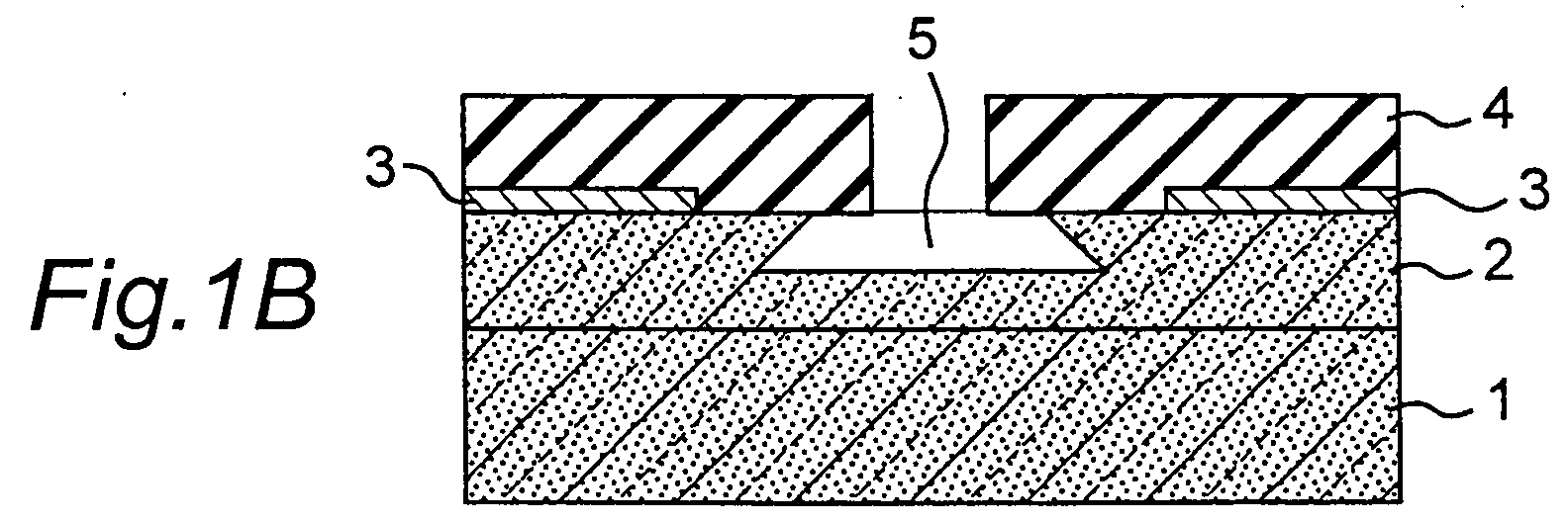
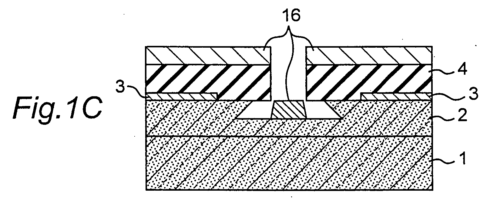
- Figs. 1A-1D are sectional views showing processes of manufacturing a GaAs field effect transistor 100 according to this embodiment.
- the producing method includes the following Steps 1 though 4.
- Step 1 As shown in Fig. 1A, source/drain electrodes 3 composed of an alloy of Au/Ge and Ni or the like, are formed on an active layer 2.
- Step 2 After forming the resist mask 4 made of novolac resin or the like, the active layer 2 is wet-etched to form recess 5 as shown in Fig. 1B.
- Step 3 Metal layer 16 composed of a stack of Ti/Al/Mo (from bottom to top) or the like is deposited on each surface of the recess 5 and resist mask 4 as shown in Fig. 1C.
- Step 4 Then, the resist mask 4 and metal layer 16 are lifted-off to create the gate electrode 6 so as to be placed on the active layer 2 at the central portion of the recess 5 as shown in Fig. 1D.
- This releasing step is performed by immersing a semi-insulating substrate 1 having a resist mask formed thereon in a resist remover at a temperature and time of about 85 degree C and about 30 minutes.
- compositions of the resist remover of this invention are amines and/or cyclic compounds containing nitrogen. They comprise from about 10 to 50 percent of 3-methyl-2-oxazolidinone (MOZ) by weight, and the rest is N-methyl-2-pyrrolidone (NMP). Preferably, the compositions are about 10 percent of MOZ by weight and about 90 percent of NMP by weight. Since NMP possesses strong polarity of its molecule, it exhibits high performance in dissolving organic chemicals without causing dissolution or corrosion of the GaAs active layer 2 and the source/drain electrodes 3 and gate electrode 6 consisted of metals.
- MOZ 3-methyl-2-oxazolidinone
- NMP N-methyl-2-pyrrolidone
- MOZ Since MOZ possesses strong polarity of its molecule, it also exhibits high performance in dissolving organic chemicals without causing dissolution or corrosion of the GaAs active layer 2 and the source/drain electrodes 3 and gate electrode 6 consisted of metals.
- compositions of the resist remover used in the producing method of this embodiment are at a predetermined ratio effective for resist removal. Due to the difference in chemical and physical properties between NMP and MOZ, combination of the compounds at ratio adequate to removal of the mask 4 is synergistically effective in lift-off process without causing corrosion or dissolution of GaAs crystal and metals.
- cyclic compounds containing nitrogen such as dimethyl piperidone, 5-methyl-2-pyrrolidone, 5-methyl-2-pyrrolidinone, N-ethyl-2-pyrrolidone, N-hydroxylethyl-2-pyrrolidone, N-cyclohexyl-2-pyrrolidone, and N-methyl- ⁇ -caprolactam, N-ethyl- ⁇ -caprolactam, are available in place of MOZ.
- the semi-insulating GaAs substrate 1 is immersed in isopropyl alcohol (IPA) and rinsed therein.
- IPA isopropyl alcohol
- Amines and/or compounds containing nitrogen need to be rinsed with isopropanol in order to avoid forming acidic species. If acidic species are generated by mixing resist removers with the cleaning solutions, an adverse problem frequently occurs: the resultant acids corrode the boundaries of the grains in the source/drain electrodes 3 to bring about decreases in recess current.
- Alcohols such as n-propyl alcohol, ethyl alcohol and methyl alcohol are also available as cleaning solutions. Isopropanol is commercially most preferable.
- the GaAs field effect transistor 100 as shown in Fig. 1D is completed.
- Fig. 2 is a SEM image showing the surface of the GaAs field effect transistor 100 produced by the asherless process.
- the image shows a gate electrode and source/drain electrodes formed on both sides thereof.
- the gate electrode formed in a recess extends from the left bottom to the right top.
- the source/drain electrodes are disposed at the both sides of the gate electrode as shown at the top of the SEM image.
- Fig. 3 shows a SEM image of a surface of GaAs FET 100 produced by the conventional resist remover containing NMP. Except for the resist remover in lift-off, the process of manufacturing the GaAs field effect transistor is the same as the above-mentioned method on the manufacturing of Fig. 100.
- Fig. 4 shows the variation of the Schottky gate performance of GaAs FETs 100, with PE-CVD SiNx dielectric film deposited as passivation, produced by the asherless method using the resist remover of this embodiment and using a conventional remover.
- the abscissa axis of n-value denotes the ideality factor and the ordinate of ⁇ b denotes the Schottky barrier height.
- the Schottky gate performances of the present invention are marked with circles, and the prior art with squares.
- the GaAs field effect transistor 100 of this embodiment has higher Schottky barrier, and has an ideality factor closer to the value of 1. As can be seen from Fig. 4, variations in characteristics among devices are improved and reduced.
- the resist remover of this embodiment is able to strip the residual organic chemicals effectively without changing the state of native oxides (i.e., surface state) on the GaAs crystal in the lift-off process, Schottky gate characteristics is enhanced and device performances such as a FET noise are improved
- the thickness of the GaAs oxides existed on the active layer is from about 4 ⁇ to about 6 ⁇ , and preferably about 5 ⁇ .
- Figs. 5A and 5B show changes in the recess current characteristics when the lift-off process is performed using a conventional resist remover including ortho-dichlorobenzene and phenol as components thereof.
- Figs. 5A and 5B show before/after characteristics of recess current in the lift-off process.
- the abscissa axis denotes voltage (Vds) applied across the source and drain
- the ordinate axis denotes current (Ids) flowing through the active GaAs.
- gateless GaAs FETs under the condition where the gate metal denoted by reference number 16 in Fig. 1 is not deposited
- This condition also applies to Figs. 6, 8, 10 and 11.
- the lift-off process is performed by immersing the semi-insulating GaAs substrate 1 into the resist remover at a temperature and time of about 80 degree C and 30 minutes.
- Other producing steps are the same as the Steps 1 through 4, namely an asherless process is used.
- the current Ids decreases when the voltage Vds ranges from 1V to 6V.
- This resist remover has aggressive ability to remove resist and thus no residual resist remains.
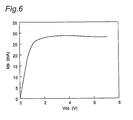
- Fig. 6 demonstrates recess current characteristics of a gateless GaAs FET after the lift-off process using the resist remover of this embodiment. Compared to the Figs. 5A and 5B, before/after recess current characteristics in Vds-Ids relation is seen to be steady in the process of this embodiment. Namely, the removing composition of this embodiment containing MOZ and NMP at a ratio and temperature and time adequate to removal of residual resists is able to prevent deterioration of recess current characteristics in the lift-off process.
- the use of a resist remover consisting of 3-methyl-2-oxazolidinone and N-methyl-2-pyrrolidone as the resist remover allows removal of a resist mask without leaving residual resist or organic substances.
- the method of producing the GaAs field effect transistor 100 of this embodiment is the same as that of the first preferred embodiment except for the resist remover used in Step 4.
- the resist mask is released using a resist remover consisting of a mixture of morpholine and N-methyl-2-pyrrolidone, cyclic compounds containing nitrogen.
- the mixture includes about 10 percent to about 50 percent of morpholine by weight and the rest of the mixture consists of N-methyl-2-pyrrolidone (NMP).
- NMP N-methyl-2-pyrrolidone
- the mixture consists of about 10 percent of morpholine by weight and about 90 percent of N-methyl-2-pyrrolidone by weight.
- This releasing step is performed by immersing the semi-insulating GaAs substrate 1 having the resist mask formed thereon into the resist remover at a temperature and time of about 85 degree C and about 30 minutes.
- the resist remover used in the producing method of this embodiment allows effective removal of the resist mask and residual resist without causing corrosion or dissolution of GaAs or metals.
- the semi-insulating substrate 1 is immersed in isopropyl alcohol (IPA) and rinsed therein.
- IPA isopropyl alcohol
- the GaAs field effect transistor 100 as shown in Fig. 1D is completed.
- Fig. 7 is a SEM image showing the surface of the GaAs field effect transistor 100 produced by the asherless process. Similar to Fig. 2, the image shows a gate electrode and source/drain electrodes formed on both sides thereof.
- the transistor has an excellent appearance having no residual resist.
- Fig. 8 is a graph showing the relation between Vds and Ids, i.e. recess current characteristics, after the lift-off process using the resist remover of this embodiment, under the condition of no gate electrode. As can be seen from Fig. 8, characteristics substantially identical with the recess current characteristics before the lift-off process shown in Fig. 5A are obtained.
- the use of the resist remover consisting of morpholine and N-methyl-2-pyrrolidone allows removal of a resist mask without leaving any residual resist, and accomplishment of an asherless process. This can prevent deterioration of various characteristics of the device caused in the ashing process, such as gate lag, changes in the gate/drain breakdown voltage, and deterioration of the FET noise. Further, variations in the recess current characteristics caused by the use of an aggressive resist remover can be prevented.
- the method of producing the GaAs field effect transistor 100 of this embodiment is the same as that of the first preferred embodiment except for the resist remover used in Step 4.
- the resist mask is released using a resist remover of a mixture consisting of dimethyl piperidone (DMPD) and N-methyl-2-pyrrolidone (NMP).
- DMPD dimethyl piperidone
- NMP N-methyl-2-pyrrolidone
- the mixture includes about 10 percent to about 50 percent of dimethyl piperidone by weight and the rest of the mixture consists of N-methyl-2-pyrrolidone.
- the mixture consists of about 10 percent of dimethyl piperidone by weight and about 90 percent of N-methyl-2-pyrrolidone by weight.
- This releasing step is performed by immersing the semi-insulating GaAs substrate 1 having the resist mask formed thereon into the resist remover at a temperature and time of about 85 degree C and about 30 minutes.
- the resist remover used in the producing method of this embodiment allows effective removal of the resist mask and residual resist without causing corrosion or dissolution of GaAs or metals.
- the semi-insulating substrate 1 is immersed in isopropyl alcohol (IPA) and rinsed therein.
- IPA isopropyl alcohol
- the GaAs field effect transistor 100 as shown in Fig. 1D is completed.
- Fig. 9 is a SEM image showing the surface of the GaAs field effect transistor 100 produced by the asherless process. Similar to Fig. 2, the image shows a gate electrode and source/drain electrodes formed on both sides thereof.
- the transistor has an excellent appearance having no residual resist.
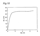
- Fig. 10 is a graph showing the relation between Vds and Ids, i.e. recess current characteristics, after the lift-off process using the resist remover of this embodiment, under the condition of no gate electrode. As can be seen from Fig. 10, characteristics substantially identical with the recess current characteristics before the lift-off process shown in Fig. 5A are obtained.
- the use of the resist remover consisting of dimethyl piperidone and N-methyl-2-pyrrolidone allows removal of a resist mask without leaving any residual resist, and accomplishment of an asherless process. This can prevent deterioration of various characteristics of the device caused in the ashing process, such as gate lag, changes in the gate/drain breakdown voltage, and deterioration of the FET noise. Further, variations in the recess current characteristics caused by the use of an aggressive resist remover can be prevented.
- the method of producing the GaAs field effect transistor 100 of this embodiment is the same as that of the first preferred embodiment except for the resist remover used in Step 4.
- the resist mask is released using a resist remover of a mixture consisting of 3-methyl-2-oxazolidinone (MOZ) and diethyl hydroxylamine.
- MOZ 3-methyl-2-oxazolidinone
- the mixture includes about 70 percent to about 90 percent of 3-methyl-2-oxazolidinone by weight and the rest of the mixture consists of diethyl hydroxylamine.
- This releasing step is performed by immersing the semi-insulating GaAs substrate 1 having the resist mask formed thereon into the resist remover at a temperature and time of about 85 degree C and about 30 minutes.
- the resist remover used in the producing method of this embodiment allows effective removal of the resist mask and residual resist without causing corrosion or dissolution of GaAs or metals.
- the semi-insulating GaAs substrate 1 is immersed in isopropyl alcohol (IPA) and rinsed therein.
- IPA isopropyl alcohol
- Using isopropyl alcohol as the cleaning solution can prevent deterioration of the characteristics of the device caused by another cleaning solution including the resist remover dissolved therein.
- the GaAs field effect transistor 100 as shown in Fig. 1D is completed.
- Fig. 11 is a graph showing the relation between Vds and Ids, i.e. recess current characteristics, after the lift-off process using the resist remover of this embodiment, under the condition of no gate electrode. As can be seen from Fig. 11, characteristics substantially identical with the recess current characteristics before the lift-off process shown in Fig. 5A are obtained.
- the use of the resist remover consisting of 3-methyl-2-oxazolidinone and diethyl hydroxylamine allows removal of a resist mask without leaving any residual resist, and accomplishment of an asherless process. This can prevent deterioration of various characteristics of the device caused in the ashing process, such as gate lag, changes in the gate/drain breakdown voltage, and deterioration of the FET noise. Further, deterioration of the recess current characteristics caused by the use of an aggressive resist remover can be prevented.
- this producing method can also be used for methods of forming an ohmic electrode of a GaAs field effect transistor such as a HEMT for example, and a base electrode and a collector electrode of an HBT. It can also be used for production of an LED or a solar cell, other than a transistor device.
- the resist removers used in the first through fourth preferred embodiments apply to the process where extremely advanced technology is required, such as a process of forming a gate electrode on an active layer.
- these resist removers can also be used for other processes, such as a step of interconnection or a step of electroplating the backside of a substrate.
- the use of these resist removers can reduce the number of kinds of resist removers required for the entire production process and thus production cost.
- this producing method can be used for production of a device made of a compound semiconductor other than GaAs.
- the use of the producing method including an asherless process according to this invention can improve the producing yield, without deteriorating the characteristics of a semiconductor device.
- the asherless process can simplify the producing process and thereby reduce producing cost.
Landscapes
- Physics & Mathematics (AREA)
- General Physics & Mathematics (AREA)
- Junction Field-Effect Transistors (AREA)
- Photosensitive Polymer And Photoresist Processing (AREA)
- Exposure Of Semiconductors, Excluding Electron Or Ion Beam Exposure (AREA)
- Drying Of Semiconductors (AREA)
- Electrodes Of Semiconductors (AREA)
Abstract

Description
The inventor has also found that the GaAs oxides deteriorates various characteristics of GaAs devices such as a gate/drain breakdown voltage, a FET noise or the like. Thus excellent GaAs semiconductor devices with no gate lag were developed. The novel idea was named "Asherless, i.e., a method without excess GaAs oxides".
Claims (9)
- A method of producing a compound semiconductor device comprising a lift-off process, the lift-off process comprising:wherein, in the releasing step, the resist mask (4) is removed sufficiently by using a resist remover essentially consisting of one or more compounds selected from a group consisting of an amines and nitrogen-including cyclic compounds so that the residual resist mask need not be removed by ashing.a step of forming a resist mask (4) having an electrode opening (5), on an active layer (2) of a compound semiconductor formed on a substrate (1) of a compound semiconductor;a step of forming a metal layer (16) on the resist mask (4) and the active layer (2) in the electrode opening (5); anda releasing step of dissolving the resist mask (4) and removing the metal layer (16) formed on the resist mask (4) to leave the metal layer (16) on the active layer (2) in the electrode opening (5) as an electrode (6);
- The producing method according to Claim 1, wherein the amine-including compound and the nitrogen-including cyclic compounds are one or more compounds selected from a group consisting of morpholine, dimethyl piperidone (DMPD), diethyl hydroxylamine (DEHA), 3-methyl-2-oxazolidinone (MOZ), and N-methyl-2-pyrrolidone.
- The producing method according to Claim 1, wherein the resist remover comprises about 10 wt % to about 50 wt % of 3-methyl-2-oxazolidinone and the rest of the resist remover consists of N-methyl-2-pyrrolidone.
- The producing method according to Claim 1, wherein the resist remover comprises about 10 wt % to about 50 wt % of morpholine and the rest of the resist remover consists of N-methyl-2-pyrrolidone.
- The producing method according to Claim 1, wherein the resist remover comprises about 10 wt % to about 50 wt % of dimethyl piperidone and the rest of the resist remover consists of N-methyl-2-pyrrolidone.
- The producing method according to Claim 1, wherein the resist remover comprises about 70 wt % to about 95 wt % of 3-methyl-2-oxazolidinone and the rest of the resist remover consists of diethyl hydroxylamine.
- The producing method according to Claim 1, further comprising a step of removing the resist remover by cleaning with isopropyl alcohol, after the releasing step.
- The producing method according to Claim 1, wherein the compound semiconductor is gallium arsenide.
- The producing method according to Claim 1, further comprising a step of forming a recess in the active layer (2), before the lift-off process;
wherein, in the releasing step, the metal layer (16) is left on the active layer (2) in the recess as a gate electrode (6).
Applications Claiming Priority (4)
| Application Number | Priority Date | Filing Date | Title |
|---|---|---|---|
| JP2002107915 | 2002-04-10 | ||
| JP2002107915 | 2002-04-10 | ||
| JP2003044236A JP4314320B2 (en) | 2002-04-10 | 2003-02-21 | Method for manufacturing compound semiconductor device |
| JP2003044236 | 2003-02-21 |
Publications (2)
| Publication Number | Publication Date |
|---|---|
| EP1363167A2 true EP1363167A2 (en) | 2003-11-19 |
| EP1363167A3 EP1363167A3 (en) | 2007-06-06 |
Family
ID=28793562
Family Applications (1)
| Application Number | Title | Priority Date | Filing Date |
|---|---|---|---|
| EP03008362A Withdrawn EP1363167A3 (en) | 2002-04-10 | 2003-04-10 | Method of producing compound semiconductor device |
Country Status (5)
| Country | Link |
|---|---|
| US (1) | US6998225B2 (en) |
| EP (1) | EP1363167A3 (en) |
| JP (1) | JP4314320B2 (en) |
| KR (1) | KR100500103B1 (en) |
| TW (1) | TWI221633B (en) |
Families Citing this family (3)
| Publication number | Priority date | Publication date | Assignee | Title |
|---|---|---|---|---|
| JP5533347B2 (en) * | 2010-06-30 | 2014-06-25 | 三菱電機株式会社 | Manufacturing method of semiconductor device |
| DE102012203003A1 (en) * | 2012-02-28 | 2013-08-29 | Schülke & Mayr GmbH | Liquid preparation for the reduction of free oxygen and the preservation of water |
| US9536966B2 (en) * | 2014-12-16 | 2017-01-03 | Transphorm Inc. | Gate structures for III-N devices |
Family Cites Families (17)
| Publication number | Priority date | Publication date | Assignee | Title |
|---|---|---|---|---|
| US4567132A (en) * | 1984-03-16 | 1986-01-28 | International Business Machines Corporation | Multi-level resist image reversal lithography process |
| DE3581659D1 (en) | 1984-05-21 | 1991-03-14 | Shipley Co | PHOTO PAINT REMOVER AND METHOD FOR REMOVING PHOTO PAINT. |
| ZA87922B (en) * | 1986-02-28 | 1987-09-30 | Macdermid Inc | Photoresist stripper composition |
| JPH0619576B2 (en) | 1986-08-21 | 1994-03-16 | 日本合成ゴム株式会社 | Stripper composition |
| US4824763A (en) * | 1987-07-30 | 1989-04-25 | Ekc Technology, Inc. | Triamine positive photoresist stripping composition and prebaking process |
| WO1990000579A1 (en) * | 1988-07-15 | 1990-01-25 | Advanced Chemical Systems International Corporation | Stripping composition using n-cyclohexyl-2-pyrrolidone |
| US5258264A (en) * | 1989-07-06 | 1993-11-02 | International Business Machines Corporation | Process of forming a dual overhang collimated lift-off stencil with subsequent metal deposition |
| US5880483A (en) * | 1990-12-18 | 1999-03-09 | Shanfield; Stanley R. | Semiconductor devices |
| JPH06188270A (en) * | 1992-12-15 | 1994-07-08 | Mitsubishi Electric Corp | Manufacture of field effect transistor and pattern transfer mask |
| JPH06260507A (en) * | 1993-03-05 | 1994-09-16 | Mitsubishi Electric Corp | Semiconductor device and manufacturing method thereof |
| JPH10335352A (en) | 1997-05-29 | 1998-12-18 | Mitsubishi Electric Corp | GaAs field effect transistor and method of manufacturing the same |
| JP3476367B2 (en) | 1998-07-27 | 2003-12-10 | 東京応化工業株式会社 | Resist stripping composition and resist stripping method using the same |
| JP4138096B2 (en) | 1998-09-09 | 2008-08-20 | 花王株式会社 | Release agent composition |
| JP2000162788A (en) * | 1998-11-27 | 2000-06-16 | Tokyo Ohka Kogyo Co Ltd | Stripping solution composition for photoresist used for copper circuit forming substrate and resist stripping method by using same |
| US6235693B1 (en) * | 1999-07-16 | 2001-05-22 | Ekc Technology, Inc. | Lactam compositions for cleaning organic and plasma etched residues for semiconductor devices |
| JP2001284230A (en) * | 2000-03-31 | 2001-10-12 | Canon Inc | Electron optical system array, charged particle beam exposure apparatus and device manufacturing method using the same |
| JP2003023015A (en) * | 2001-07-06 | 2003-01-24 | Mitsubishi Electric Corp | GaAs based semiconductor field effect transistor |
-
2003
- 2003-02-21 JP JP2003044236A patent/JP4314320B2/en not_active Expired - Fee Related
- 2003-04-07 KR KR20030021749A patent/KR100500103B1/en not_active Expired - Fee Related
- 2003-04-08 TW TW092107987A patent/TWI221633B/en not_active IP Right Cessation
- 2003-04-09 US US10/409,079 patent/US6998225B2/en not_active Expired - Fee Related
- 2003-04-10 EP EP03008362A patent/EP1363167A3/en not_active Withdrawn
Also Published As
| Publication number | Publication date |
|---|---|
| KR100500103B1 (en) | 2005-07-11 |
| TW200405420A (en) | 2004-04-01 |
| US6998225B2 (en) | 2006-02-14 |
| JP4314320B2 (en) | 2009-08-12 |
| KR20030081058A (en) | 2003-10-17 |
| TWI221633B (en) | 2004-10-01 |
| EP1363167A3 (en) | 2007-06-06 |
| JP2004004569A (en) | 2004-01-08 |
| US20030194656A1 (en) | 2003-10-16 |
Similar Documents
| Publication | Publication Date | Title |
|---|---|---|
| JP5817139B2 (en) | Method for manufacturing compound semiconductor device and cleaning agent | |
| CN1320165C (en) | Method for cleaning substrate and cleaning solution | |
| US6852615B2 (en) | Ohmic contacts for high electron mobility transistors and a method of making the same | |
| US5112763A (en) | Process for forming a Schottky barrier gate | |
| US6998225B2 (en) | Method of producing compound semiconductor device | |
| KR0163833B1 (en) | Method of fabricating semiconductor device | |
| US4581076A (en) | Selectively implanting GaAs semiconductor substrates through a metallic layer | |
| JP2012178458A (en) | Method of manufacturing semiconductor device and method of cleaning semiconductor substrate | |
| JPS60111474A (en) | Manufacture of semiconductor device | |
| CN101447450B (en) | Method for manufacturing monolithic integrated GaAs-based MHEMT and PIN diode | |
| CN1808707A (en) | Manufacturing method of resonant-tunneling diode and high-electron mobility transistor components | |
| CN101447449B (en) | Method for manufacturing monolithic integrated GaAs-based PHEMT and PIN diode | |
| JP2699950B2 (en) | Method for manufacturing compound semiconductor device | |
| US20050142702A1 (en) | Semiconductor device and manufacturing method thereof | |
| JP2667840B2 (en) | Method for manufacturing compound semiconductor device | |
| JPH08124939A (en) | Method for manufacturing semiconductor device | |
| CN1649101A (en) | Manufacturing method for compound semiconductor device | |
| EP0366939A2 (en) | A process for forming a Schottky barrier gate on gallium-arsenide | |
| JPH04102326A (en) | Semiconductor device and manufacture thereof | |
| JPH063814B2 (en) | Method for manufacturing semiconductor device | |
| JPH0410629A (en) | Manufacture of semiconductor device | |
| JPS62232968A (en) | Manufacture of semiconductor device | |
| Badawi et al. | Ion implantation in semiconductor bodies | |
| JPH03126231A (en) | Method for manufacturing field effect transistors | |
| JPS6158274A (en) | Manufacture of semiconductor device |
Legal Events
| Date | Code | Title | Description |
|---|---|---|---|
| PUAI | Public reference made under article 153(3) epc to a published international application that has entered the european phase |
Free format text: ORIGINAL CODE: 0009012 |
|
| AK | Designated contracting states |
Kind code of ref document: A2 Designated state(s): AT BE BG CH CY CZ DE DK EE ES FI FR GB GR HU IE IT LI LU MC NL PT SE SI SK TR |
|
| AX | Request for extension of the european patent |
Extension state: AL LT LV MK RO |
|
| RAP1 | Party data changed (applicant data changed or rights of an application transferred) |
Owner name: EKC TECHNOLOGY KABUSHIKI KAISHA Owner name: MITSUBISHI DENKI KABUSHIKI KAISHA |
|
| PUAL | Search report despatched |
Free format text: ORIGINAL CODE: 0009013 |
|
| RIC1 | Information provided on ipc code assigned before grant |
Ipc: H01L 21/338 20060101ALI20070423BHEP Ipc: G03F 7/42 20060101AFI20030927BHEP |
|
| AK | Designated contracting states |
Kind code of ref document: A3 Designated state(s): AT BE BG CH CY CZ DE DK EE ES FI FR GB GR HU IE IT LI LU MC NL PT SE SI SK TR |
|
| AX | Request for extension of the european patent |
Extension state: AL LT LV MK RO |
|
| 17P | Request for examination filed |
Effective date: 20071205 |
|
| AKX | Designation fees paid |
Designated state(s): DE FR GB |
|
| 17Q | First examination report despatched |
Effective date: 20090407 |
|
| RAP1 | Party data changed (applicant data changed or rights of an application transferred) |
Owner name: EKC TECHNOLOGY, INC. Owner name: MITSUBISHI DENKI KABUSHIKI KAISHA |
|
| RAP1 | Party data changed (applicant data changed or rights of an application transferred) |
Owner name: MITSUBISHI DENKI KABUSHIKI KAISHA |
|
| RIC1 | Information provided on ipc code assigned before grant |
Ipc: H01L 29/423 20060101ALI20120221BHEP Ipc: H01L 21/335 20060101ALI20120221BHEP Ipc: H01L 21/331 20060101ALI20120221BHEP Ipc: H01L 21/285 20060101ALI20120221BHEP Ipc: H01L 21/338 20060101ALI20120221BHEP Ipc: G03F 7/42 20060101AFI20120221BHEP |
|
| GRAP | Despatch of communication of intention to grant a patent |
Free format text: ORIGINAL CODE: EPIDOSNIGR1 |
|
| STAA | Information on the status of an ep patent application or granted ep patent |
Free format text: STATUS: THE APPLICATION IS DEEMED TO BE WITHDRAWN |
|
| 18D | Application deemed to be withdrawn |
Effective date: 20120829 |