EP1362396B1 - Resonant reflector for use with optoelectronic devices - Google Patents
Resonant reflector for use with optoelectronic devices Download PDFInfo
- Publication number
- EP1362396B1 EP1362396B1 EP01994296A EP01994296A EP1362396B1 EP 1362396 B1 EP1362396 B1 EP 1362396B1 EP 01994296 A EP01994296 A EP 01994296A EP 01994296 A EP01994296 A EP 01994296A EP 1362396 B1 EP1362396 B1 EP 1362396B1
- Authority
- EP
- European Patent Office
- Prior art keywords
- waveguide
- grating
- cladding
- buffer layer
- mirror
- Prior art date
- Legal status (The legal status is an assumption and is not a legal conclusion. Google has not performed a legal analysis and makes no representation as to the accuracy of the status listed.)
- Expired - Lifetime
Links
- 230000005693 optoelectronics Effects 0.000 title claims abstract description 49
- 239000000758 substrate Substances 0.000 claims abstract description 48
- 238000000034 method Methods 0.000 claims abstract description 17
- 238000005253 cladding Methods 0.000 claims description 56
- 230000003287 optical effect Effects 0.000 claims description 13
- 229910001218 Gallium arsenide Inorganic materials 0.000 claims description 12
- 230000001902 propagating effect Effects 0.000 claims description 8
- VYPSYNLAJGMNEJ-UHFFFAOYSA-N Silicium dioxide Chemical compound O=[Si]=O VYPSYNLAJGMNEJ-UHFFFAOYSA-N 0.000 claims description 7
- 239000004593 Epoxy Substances 0.000 claims description 6
- 229910052681 coesite Inorganic materials 0.000 claims description 3
- 229910052906 cristobalite Inorganic materials 0.000 claims description 3
- 239000000377 silicon dioxide Substances 0.000 claims description 3
- 229910052682 stishovite Inorganic materials 0.000 claims description 3
- 229910052905 tridymite Inorganic materials 0.000 claims description 3
- 238000005530 etching Methods 0.000 claims description 2
- 229910000980 Aluminium gallium arsenide Inorganic materials 0.000 claims 4
- TWNQGVIAIRXVLR-UHFFFAOYSA-N oxo(oxoalumanyloxy)alumane Chemical compound O=[Al]O[Al]=O TWNQGVIAIRXVLR-UHFFFAOYSA-N 0.000 claims 1
- 229910052814 silicon oxide Inorganic materials 0.000 claims 1
- 238000002955 isolation Methods 0.000 abstract description 7
- FTWRSWRBSVXQPI-UHFFFAOYSA-N alumanylidynearsane;gallanylidynearsane Chemical compound [As]#[Al].[As]#[Ga] FTWRSWRBSVXQPI-UHFFFAOYSA-N 0.000 description 18
- JBRZTFJDHDCESZ-UHFFFAOYSA-N AsGa Chemical compound [As]#[Ga] JBRZTFJDHDCESZ-UHFFFAOYSA-N 0.000 description 12
- 239000004065 semiconductor Substances 0.000 description 11
- 238000002310 reflectometry Methods 0.000 description 10
- 230000010287 polarization Effects 0.000 description 8
- 230000008901 benefit Effects 0.000 description 7
- 230000003595 spectral effect Effects 0.000 description 7
- 239000000463 material Substances 0.000 description 6
- 238000004519 manufacturing process Methods 0.000 description 5
- 229910052751 metal Inorganic materials 0.000 description 5
- 239000002184 metal Substances 0.000 description 5
- 238000010521 absorption reaction Methods 0.000 description 4
- 238000013459 approach Methods 0.000 description 4
- 239000007943 implant Substances 0.000 description 4
- 125000006850 spacer group Chemical group 0.000 description 4
- 238000013461 design Methods 0.000 description 3
- 239000012535 impurity Substances 0.000 description 3
- 238000005468 ion implantation Methods 0.000 description 3
- GWEVSGVZZGPLCZ-UHFFFAOYSA-N Titan oxide Chemical compound O=[Ti]=O GWEVSGVZZGPLCZ-UHFFFAOYSA-N 0.000 description 2
- MCMNRKCIXSYSNV-UHFFFAOYSA-N Zirconium dioxide Chemical compound O=[Zr]=O MCMNRKCIXSYSNV-UHFFFAOYSA-N 0.000 description 2
- MDPILPRLPQYEEN-UHFFFAOYSA-N aluminium arsenide Chemical compound [As]#[Al] MDPILPRLPQYEEN-UHFFFAOYSA-N 0.000 description 2
- 239000011248 coating agent Substances 0.000 description 2
- 238000000576 coating method Methods 0.000 description 2
- 238000004891 communication Methods 0.000 description 2
- 238000005516 engineering process Methods 0.000 description 2
- -1 AlxGa1-xAs Chemical class 0.000 description 1
- 229910000530 Gallium indium arsenide Inorganic materials 0.000 description 1
- 229910052581 Si3N4 Inorganic materials 0.000 description 1
- 229910052782 aluminium Inorganic materials 0.000 description 1
- XAGFODPZIPBFFR-UHFFFAOYSA-N aluminium Chemical compound [Al] XAGFODPZIPBFFR-UHFFFAOYSA-N 0.000 description 1
- 230000002547 anomalous effect Effects 0.000 description 1
- 239000006117 anti-reflective coating Substances 0.000 description 1
- 230000003667 anti-reflective effect Effects 0.000 description 1
- 238000003491 array Methods 0.000 description 1
- 230000004888 barrier function Effects 0.000 description 1
- 230000009286 beneficial effect Effects 0.000 description 1
- 230000015556 catabolic process Effects 0.000 description 1
- 239000002800 charge carrier Substances 0.000 description 1
- 150000001875 compounds Chemical class 0.000 description 1
- 238000010276 construction Methods 0.000 description 1
- 230000003247 decreasing effect Effects 0.000 description 1
- 238000006731 degradation reaction Methods 0.000 description 1
- 238000010586 diagram Methods 0.000 description 1
- 230000000694 effects Effects 0.000 description 1
- 239000000835 fiber Substances 0.000 description 1
- 238000001914 filtration Methods 0.000 description 1
- CJNBYAVZURUTKZ-UHFFFAOYSA-N hafnium(IV) oxide Inorganic materials O=[Hf]=O CJNBYAVZURUTKZ-UHFFFAOYSA-N 0.000 description 1
- 238000001093 holography Methods 0.000 description 1
- 238000003384 imaging method Methods 0.000 description 1
- 238000002513 implantation Methods 0.000 description 1
- 230000010354 integration Effects 0.000 description 1
- 238000001459 lithography Methods 0.000 description 1
- 238000005259 measurement Methods 0.000 description 1
- 238000001451 molecular beam epitaxy Methods 0.000 description 1
- 230000003647 oxidation Effects 0.000 description 1
- 238000007254 oxidation reaction Methods 0.000 description 1
- 230000001590 oxidative effect Effects 0.000 description 1
- 238000002161 passivation Methods 0.000 description 1
- 230000000737 periodic effect Effects 0.000 description 1
- 238000012797 qualification Methods 0.000 description 1
- 230000035945 sensitivity Effects 0.000 description 1
- 238000004611 spectroscopical analysis Methods 0.000 description 1
- 238000000927 vapour-phase epitaxy Methods 0.000 description 1
Images


Classifications
-
- H—ELECTRICITY
- H01—ELECTRIC ELEMENTS
- H01S—DEVICES USING THE PROCESS OF LIGHT AMPLIFICATION BY STIMULATED EMISSION OF RADIATION [LASER] TO AMPLIFY OR GENERATE LIGHT; DEVICES USING STIMULATED EMISSION OF ELECTROMAGNETIC RADIATION IN WAVE RANGES OTHER THAN OPTICAL
- H01S5/00—Semiconductor lasers
- H01S5/10—Construction or shape of the optical resonator, e.g. extended or external cavity, coupled cavities, bent-guide, varying width, thickness or composition of the active region
- H01S5/18—Surface-emitting [SE] lasers, e.g. having both horizontal and vertical cavities
- H01S5/183—Surface-emitting [SE] lasers, e.g. having both horizontal and vertical cavities having only vertical cavities, e.g. vertical cavity surface-emitting lasers [VCSEL]
- H01S5/18355—Surface-emitting [SE] lasers, e.g. having both horizontal and vertical cavities having only vertical cavities, e.g. vertical cavity surface-emitting lasers [VCSEL] having a defined polarisation
-
- H—ELECTRICITY
- H01—ELECTRIC ELEMENTS
- H01S—DEVICES USING THE PROCESS OF LIGHT AMPLIFICATION BY STIMULATED EMISSION OF RADIATION [LASER] TO AMPLIFY OR GENERATE LIGHT; DEVICES USING STIMULATED EMISSION OF ELECTROMAGNETIC RADIATION IN WAVE RANGES OTHER THAN OPTICAL
- H01S5/00—Semiconductor lasers
- H01S5/10—Construction or shape of the optical resonator, e.g. extended or external cavity, coupled cavities, bent-guide, varying width, thickness or composition of the active region
- H01S5/18—Surface-emitting [SE] lasers, e.g. having both horizontal and vertical cavities
- H01S5/183—Surface-emitting [SE] lasers, e.g. having both horizontal and vertical cavities having only vertical cavities, e.g. vertical cavity surface-emitting lasers [VCSEL]
-
- H—ELECTRICITY
- H01—ELECTRIC ELEMENTS
- H01S—DEVICES USING THE PROCESS OF LIGHT AMPLIFICATION BY STIMULATED EMISSION OF RADIATION [LASER] TO AMPLIFY OR GENERATE LIGHT; DEVICES USING STIMULATED EMISSION OF ELECTROMAGNETIC RADIATION IN WAVE RANGES OTHER THAN OPTICAL
- H01S5/00—Semiconductor lasers
- H01S5/10—Construction or shape of the optical resonator, e.g. extended or external cavity, coupled cavities, bent-guide, varying width, thickness or composition of the active region
- H01S5/11—Comprising a photonic bandgap structure
-
- H—ELECTRICITY
- H01—ELECTRIC ELEMENTS
- H01S—DEVICES USING THE PROCESS OF LIGHT AMPLIFICATION BY STIMULATED EMISSION OF RADIATION [LASER] TO AMPLIFY OR GENERATE LIGHT; DEVICES USING STIMULATED EMISSION OF ELECTROMAGNETIC RADIATION IN WAVE RANGES OTHER THAN OPTICAL
- H01S5/00—Semiconductor lasers
- H01S5/10—Construction or shape of the optical resonator, e.g. extended or external cavity, coupled cavities, bent-guide, varying width, thickness or composition of the active region
- H01S5/18—Surface-emitting [SE] lasers, e.g. having both horizontal and vertical cavities
- H01S5/183—Surface-emitting [SE] lasers, e.g. having both horizontal and vertical cavities having only vertical cavities, e.g. vertical cavity surface-emitting lasers [VCSEL]
- H01S5/18308—Surface-emitting [SE] lasers, e.g. having both horizontal and vertical cavities having only vertical cavities, e.g. vertical cavity surface-emitting lasers [VCSEL] having a special structure for lateral current or light confinement
- H01S5/18319—Surface-emitting [SE] lasers, e.g. having both horizontal and vertical cavities having only vertical cavities, e.g. vertical cavity surface-emitting lasers [VCSEL] having a special structure for lateral current or light confinement comprising a periodical structure in lateral directions
-
- H—ELECTRICITY
- H01—ELECTRIC ELEMENTS
- H01S—DEVICES USING THE PROCESS OF LIGHT AMPLIFICATION BY STIMULATED EMISSION OF RADIATION [LASER] TO AMPLIFY OR GENERATE LIGHT; DEVICES USING STIMULATED EMISSION OF ELECTROMAGNETIC RADIATION IN WAVE RANGES OTHER THAN OPTICAL
- H01S5/00—Semiconductor lasers
- H01S5/10—Construction or shape of the optical resonator, e.g. extended or external cavity, coupled cavities, bent-guide, varying width, thickness or composition of the active region
- H01S5/18—Surface-emitting [SE] lasers, e.g. having both horizontal and vertical cavities
- H01S5/183—Surface-emitting [SE] lasers, e.g. having both horizontal and vertical cavities having only vertical cavities, e.g. vertical cavity surface-emitting lasers [VCSEL]
- H01S5/18358—Surface-emitting [SE] lasers, e.g. having both horizontal and vertical cavities having only vertical cavities, e.g. vertical cavity surface-emitting lasers [VCSEL] containing spacer layers to adjust the phase of the light wave in the cavity
-
- H—ELECTRICITY
- H01—ELECTRIC ELEMENTS
- H01S—DEVICES USING THE PROCESS OF LIGHT AMPLIFICATION BY STIMULATED EMISSION OF RADIATION [LASER] TO AMPLIFY OR GENERATE LIGHT; DEVICES USING STIMULATED EMISSION OF ELECTROMAGNETIC RADIATION IN WAVE RANGES OTHER THAN OPTICAL
- H01S5/00—Semiconductor lasers
- H01S5/10—Construction or shape of the optical resonator, e.g. extended or external cavity, coupled cavities, bent-guide, varying width, thickness or composition of the active region
- H01S5/18—Surface-emitting [SE] lasers, e.g. having both horizontal and vertical cavities
- H01S5/183—Surface-emitting [SE] lasers, e.g. having both horizontal and vertical cavities having only vertical cavities, e.g. vertical cavity surface-emitting lasers [VCSEL]
- H01S5/18361—Structure of the reflectors, e.g. hybrid mirrors
- H01S5/18369—Structure of the reflectors, e.g. hybrid mirrors based on dielectric materials
-
- H—ELECTRICITY
- H01—ELECTRIC ELEMENTS
- H01S—DEVICES USING THE PROCESS OF LIGHT AMPLIFICATION BY STIMULATED EMISSION OF RADIATION [LASER] TO AMPLIFY OR GENERATE LIGHT; DEVICES USING STIMULATED EMISSION OF ELECTROMAGNETIC RADIATION IN WAVE RANGES OTHER THAN OPTICAL
- H01S5/00—Semiconductor lasers
- H01S5/10—Construction or shape of the optical resonator, e.g. extended or external cavity, coupled cavities, bent-guide, varying width, thickness or composition of the active region
- H01S5/18—Surface-emitting [SE] lasers, e.g. having both horizontal and vertical cavities
- H01S5/183—Surface-emitting [SE] lasers, e.g. having both horizontal and vertical cavities having only vertical cavities, e.g. vertical cavity surface-emitting lasers [VCSEL]
- H01S5/18361—Structure of the reflectors, e.g. hybrid mirrors
- H01S5/18377—Structure of the reflectors, e.g. hybrid mirrors comprising layers of different kind of materials, e.g. combinations of semiconducting with dielectric or metallic layers
-
- H—ELECTRICITY
- H01—ELECTRIC ELEMENTS
- H01S—DEVICES USING THE PROCESS OF LIGHT AMPLIFICATION BY STIMULATED EMISSION OF RADIATION [LASER] TO AMPLIFY OR GENERATE LIGHT; DEVICES USING STIMULATED EMISSION OF ELECTROMAGNETIC RADIATION IN WAVE RANGES OTHER THAN OPTICAL
- H01S5/00—Semiconductor lasers
- H01S5/10—Construction or shape of the optical resonator, e.g. extended or external cavity, coupled cavities, bent-guide, varying width, thickness or composition of the active region
- H01S5/18—Surface-emitting [SE] lasers, e.g. having both horizontal and vertical cavities
- H01S5/183—Surface-emitting [SE] lasers, e.g. having both horizontal and vertical cavities having only vertical cavities, e.g. vertical cavity surface-emitting lasers [VCSEL]
- H01S5/18386—Details of the emission surface for influencing the near- or far-field, e.g. a grating on the surface
- H01S5/18388—Lenses
-
- H—ELECTRICITY
- H01—ELECTRIC ELEMENTS
- H01S—DEVICES USING THE PROCESS OF LIGHT AMPLIFICATION BY STIMULATED EMISSION OF RADIATION [LASER] TO AMPLIFY OR GENERATE LIGHT; DEVICES USING STIMULATED EMISSION OF ELECTROMAGNETIC RADIATION IN WAVE RANGES OTHER THAN OPTICAL
- H01S5/00—Semiconductor lasers
- H01S5/10—Construction or shape of the optical resonator, e.g. extended or external cavity, coupled cavities, bent-guide, varying width, thickness or composition of the active region
- H01S5/18—Surface-emitting [SE] lasers, e.g. having both horizontal and vertical cavities
- H01S5/183—Surface-emitting [SE] lasers, e.g. having both horizontal and vertical cavities having only vertical cavities, e.g. vertical cavity surface-emitting lasers [VCSEL]
- H01S5/18397—Plurality of active layers vertically stacked in a cavity for multi-wavelength emission
-
- H—ELECTRICITY
- H01—ELECTRIC ELEMENTS
- H01S—DEVICES USING THE PROCESS OF LIGHT AMPLIFICATION BY STIMULATED EMISSION OF RADIATION [LASER] TO AMPLIFY OR GENERATE LIGHT; DEVICES USING STIMULATED EMISSION OF ELECTROMAGNETIC RADIATION IN WAVE RANGES OTHER THAN OPTICAL
- H01S5/00—Semiconductor lasers
- H01S5/40—Arrangement of two or more semiconductor lasers, not provided for in groups H01S5/02 - H01S5/30
- H01S5/4025—Array arrangements, e.g. constituted by discrete laser diodes or laser bar
- H01S5/4087—Array arrangements, e.g. constituted by discrete laser diodes or laser bar emitting more than one wavelength
-
- H—ELECTRICITY
- H01—ELECTRIC ELEMENTS
- H01S—DEVICES USING THE PROCESS OF LIGHT AMPLIFICATION BY STIMULATED EMISSION OF RADIATION [LASER] TO AMPLIFY OR GENERATE LIGHT; DEVICES USING STIMULATED EMISSION OF ELECTROMAGNETIC RADIATION IN WAVE RANGES OTHER THAN OPTICAL
- H01S5/00—Semiconductor lasers
- H01S5/40—Arrangement of two or more semiconductor lasers, not provided for in groups H01S5/02 - H01S5/30
- H01S5/42—Arrays of surface emitting lasers
- H01S5/423—Arrays of surface emitting lasers having a vertical cavity
Definitions
- This invention relates to the field of optoelectronic devices, and more particularly to resonant reflectors for use with optoelectronic devices.
- semiconductor photodiodes Various forms of optoelectronic devices have been developed and have found widespread use including, for example, semiconductor photodiodes, semiconductor photo detectors, etc.
- Semiconductor lasers have found widespread use in modem technology as the light source of choice for various devices, e.g., communication systems, compact disc players, and so on.
- a semiconductor laser is coupled to a semiconductor detector (e.g., photodiode) through a fiber optic link or even free space. This configuration provides a high-speed communication path, which, for many applications, can be extremely beneficial.
- a typical edge-emitting semiconductor laser is a double heterostructure with a narrow bandgap, high refractive index layer surrounded on opposed major surfaces by wide bandgap, low refractive index layers often called cladding layers.
- the low bandgap layer is termed the "active layer", and the cladding layers serve to confine both charge carriers and optical energy in the active layer or region.
- Opposite ends of the active layer have mirror facets which form the laser cavity. When current is passed through the structure, electrons and holes combine in the active layer to generate light.
- CMOS complementary metal-oxide-semiconductor
- VCSEL Vertical Cavity Surface Emitting Lasers
- U.S. Patent No. 5,115,442 by Yong H. Lee et al., issued May 19, 1992, and entitled “Top-emitting Surface Emitting Laser Structures” and U.S. Patent No. 5,475,701, issued on December 12, 1995 to Mary K. Hibbs-Brenner, and entitled “Integrated Laser Power Monitor”.
- VCSEL Vertical Cavity Surface Emitting Lasers
- Vertical Cavity Surface Emitting Lasers offer numerous performance and potential producibility advantages over conventional edge emitting lasers. These include many benefits associated with their geometry, including their amenability to one- and two-dimensional arrays, wafer-level qualification, and desirable beam characteristics, typically circularly symmetric low-divergence beams.
- VCSELs typically have an active region having bulk or one or more quantum well layers.
- mirror stacks On opposite sides of the active region are mirror stacks, often formed by interleaved semiconductor layers each a quarter wavelength thick at the desired operating wavelength (in the medium).
- the mirror stacks are typically of opposite conductivity type on either side of the active region, and the laser is typically turned on and off by varying the current through the mirror stacks and the active region.
- VCSELs High-yield, high performance VCSELs have been demonstrated and exploited in commercialization. Top-surface-emitting AlGaAs-based VCSELs are producible in a manner analogous to semiconductor integrated circuits, and are amenable to low-cost high-volume manufacture and integration with existing electronics technology platforms. Moreover, VCSEL uniformity and reproducibility have been demonstrated using a standard, unmodified commercially available metal organic vapor phase epitaxy (MOVPE) chamber and molecular beam epitaxy (MBE) giving very high device yields.
- MOVPE metal organic vapor phase epitaxy
- MBE molecular beam epitaxy
- VCSELs are expected to provide a performance and cost advantage in fast (e.g., Gbits/s) medium distance (e.g., up to approximately 1000 meters) single or multi-channel data link applications, and numerous optical and/or imaging applications. This results from their inherent geometry, which provides potential low-cost high performance transmitters with flexible and desirable characteristics.
- a related photodetector is known as a resonant cavity photo detector (RCPD).
- Resonant cavity photodetectors are typically constructed similar to VCSELs, but operate in a reverse bias mode.
- a resonant cavity photodetector may be more efficient than a standard photodiode because the light that enters the optical cavity, through one of the mirrors, may be effectively reflected through the active region many times. The light may thus be reflected between the mirror stacks until the light is either absorbed by the active region or until it escapes through one of the mirror stacks. Because the mirror stacks are typically highly reflective near resonance, most of the light that enters the cavity is absorbed by the active region.
- the top and/or bottom mirror stacks are Distributed Bragg Reflector (DBR) mirrors.
- DBR mirrors typically include a number of alternating layers of semiconductor material such as AlGaA5 and AlAs.
- both the top and bottom mirror stacks include a significant number of DBR mirror periods to achieve the desired reflectance.
- One way to reduce the number of DBR mirror periods that are required is to replace some of the DBR mirror periods with a resonant reflector.
- a typical resonant reflector may include, among other things, a waveguide and a grating.
- US-A-6055262 discloses a VCSEL with a resonant reflector combined with a DBR.
- the present invention overcomes many of the disadvantages of the prior art by providing an optoelectronic device that provides isolation between a resonant reflector and an adjacent conducting layer of the optoelectronic device.
- an optoelectronic device comprising:
- a monolithic transceiver having a light emitting device and a light receiving device, comprising:
- a device comprising:
- an optoelectronic device comprising:
- Figure 1 is a schematic illustration of a planar, current-guided, GaAs/AlGaAs top surface emitting vertical cavity laser 10 in accordance with the prior art.
- n-doped gallium arsenide (GaAs) substrate 14 is a n-contact 12.
- substrate 14 is doped with impurities of a first type (i.e., n type).
- An n-type mirror stack 16 is formed on substrate 14.
- Spacer 18 has a bottom confinement layer 20 and a top confinement layer 24 surrounding active region 22.
- a p-type mirror stack 26 is formed on top confinement layer 24.
- a p-metal layer 28 is formed on stack 26.
- the emission region may have a passivation layer 30.
- Isolation region 29 restricts the area of the current flow 27 through the active region.
- Region 29 may be formed by deep H+ ion implantation. While a deep H+ implant is provided as an illustration, it is contemplated that any type of current and field confinement may be used, including for example, gain-guided, oxide-confinement, or any other means.
- the diameter "g" may be set to provide the desired active area, and thus the gain aperture of the VCSEL 10. Further, the diameter "g” may be set by the desired resistance of the p-type mirror stack 26, particularly through the non-conductive region 29. Thus, non-conductive region 29 performs the gain guiding function.
- the diameter "g" is typically limited by fabrication limitations, such as lateral straggle during the implantation step.
- Spacer 18 may contain a bulk or quantum-well active region disposed between mirror stacks 16 and 26.
- Stacks 16 and 26 are distributed Bragg reflector (DBR) stacks, and may include periodic layers of doped AlGaAs and aluminum arsenide (AlAs).
- DBR distributed Bragg reflector
- the AlGaAs of stack 16 is doped with the same type of impurity as substrate 14 (e.g., n type), and the AlGaAs of stack 26 is doped with the other kind of impurity (e.g., p type).
- Metal contact layers 12 and 28 are ohmic contacts that allow appropriate electrical biasing of laser diode 10.
- laser diode 10 When laser diode 10 is forward biased with a more positive voltage on contact 28 than on contact 12, active region 22 emits light 31 which passes through stack 26.
- a typical near IR VCSEL requires high reflectivity (>99%).
- an all-semiconductor DBR typically requires 20 - 40 mirror periods with a thickness of 2 - 4 ⁇ m.
- the epi-structure required for a complete VCSEL, including both top and bottom DBR mirrors surrounding an active spacer region typically includes over 200 layers having a thickness in excess of 7 - 8 ⁇ m.
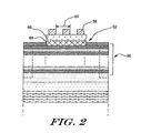
- FIG. 2 is a schematic cross-sectional side view of a planar, current-guided, GaAs/AlGaAs top surface emitting vertical cavity laser with a hybrid top mirror including a resonant reflector 52 and a distributed Bragg reflector 56.
- This device combines the anomalous filtering properties of guided mode resonance in a dielectric waveguide grating with the reflective properties of a conventional DBR mirror.
- the hybrid mirror structure includes, for example, a resonant reflector 52 and a DBR mirror 56.
- the bottom mirror may also include a resonant reflector structure, if desired.
- a dielectric resonant reflector 52 is highly reflective on resonance, and may be more reflective than a corresponding DBR type mirror at the same wavelength.
- the number of DBR mirror periods needed for a given reflectance may be reduced.
- lateral straggle effects during ion implantation of the gain guiding region 62 through the DBR mirrors often limits the lateral dimension 64 of the active region to ⁇ 10 ⁇ m. This directly impacts the minimum achievable threshold current, single mode operation, and indirectly impacts the speed of the VCSEL.
- a resonant reflector into the top mirror, equivalent or superior reflectance properties in a structure five to ten times thinner may be achieved. This may translate into an ion implant that is more controllable, which may reduce the volume of the active region.
- a smaller active region may reduce the operating current and power of the device, improve planarity and thus the monolithic integrability of the VCSEL with electronics and smart pixels, and may provide a controllable single mode and single polarization emission with increased modal control.
- the hybrid approach of Figure 2 is compatible with alternate existing gain-guiding techniques including etched pillars (with or without planarization and/or regrowth), lateral oxidation, selective growth, etc.
- the resonant reflector may improve the processiblility and performance of the alternate current guiding approaches. While ion implantation is provided as an illustration, it is contemplated that any type of current and field confinement may be used, including for example, gain-guided, oxide-confinement, or any other means.
- the resonant reflector 52 of Figure 2 includes a three layer waveguide-grating structure suitable for use in a near IR VCSEL.
- the three-layer stack may be designed to function both as an anti-reflection (AR) coating near the emission wavelength for the VCSEL-structure substrate and independently as a guided-mode resonant reflector waveguide-grating.
- the three layers of resonant reflector 52 may form an anti-reflective region, which provides little reflectance for at least a predetermined range of wavelengths including a resonant wavelength.
- the grating multilayer waveguide structure shown at 52 causes the structure to become substantially more reflective, at least at the resonant wavelength.
- the three-layer stack 52 may be designed to function both as a high-reflectivity coating for the VCSEL-structure substrate and independently as a guided-mode resonant reflector waveguide-grating.
- the three-layer structure 52 forms a highly-reflective mirror region which provides reflectance for at least a predetermined range of wavelengths including a resonant wavelength (e.g., near 980 nm).
- the overall reflectance of the top mirror, including layers 66 and 68 may be less than that required for lasing. This may be accomplished by, for example, reducing the number of mirror periods in the top DBR mirror 56.
- Grating layer 58 causes the guided mode resonant reflector structure 52 to become substantially more reflective at least near the resonant wavelength. In either case, the number of DBR mirror layers beneath the resonant reflector 52 may be reduced relative to the conventional VCSEL construction shown in Figure 1.
- Resonance is achieved in the resonance reflector 52 by matching the first-diffraction order wave vector of the grating 58 to the propagating mode of the waveguide 66. Since the latter depends on polarization, the reflectance is inherently polarization-selective.
- the resonant wavelength is determined primarily by the grating period 60, and the bandwidth is determined primarily by the modulation of the refractive index and fill factor of the grating 58.
- the top layer, middle layer and bottom layer are formed from IndiumTinOxide (ITO), GaAs, and AlGaAs, respectively.
- the refraction indices for the top, middle and bottom layers are 1.96, 3.5 and 3.24, respectively, and the thicknesses of the top, middle and bottom layers are preferably ⁇ /4, ⁇ /4 and ⁇ /4, respectively.
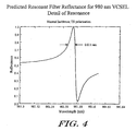
- the layers are placed on a substrate with an effective reflective index of 3.2. This structure is simulated to exhibit one transverse Electric (TE) mode resonance (with a polarization parallel to the grating), no perpendicular resonance and a low out of resonant reflectance near 10 -6 .
- TE transverse Electric
- the imaginary component "k" of the refractive index is related to optical absorption and electrical conductivity of the resonant reflector.
- This graph illustrates the extreme sensitivity of the resonant reflector 52 to absorption, or more generally, to loss of any kind.
- the conductivity of the resonant reflector should also be zero (e.g., non-conductive).
- the present invention contemplates isolating the resonant reflector from adjacent conducting layers. Isolation is preferably accomplished by providing a non-conductive (e.g. dielectric) buffer or cladding layer between the resonant reflector and the adjacent conducting layer of the optoelectronic device.
- the non-conductive cladding or buffer layer is preferably sufficiently thick, and/or has a sufficiently low refractive index relative to the refractive index of the waveguide of the resonant reflector, to substantially prevent energy in the evanescent tail of the guided mode in the waveguide from entering the adjacent conductive layer of the optoelectronic device.
- the waveguide is formed from a dielectric that has a higher refractive index than the refractive index of the buffer or cladding layer, and also higher than the average refractive index of the grating.
- the thickness of the waveguide preferably depends on the refractive index difference between the waveguide and the buffer or cladding layer.
- Figure 6 is a schematic cross-sectional side view of a planar, current-guided, GaAs/AlGaAs top surface emitting vertical cavity laser with a cladding or buffer layer 80 interposed between the waveguide layer 82 of the resonant reflector 84 and the top DBR mirror 86.
- the cladding or buffer layer 80 is preferably sufficiently thick, and/or has a sufficiently low refractive index relative to the refractive index of the waveguide of the resonant reflector, to substantially prevent energy in the evanescent tail of the guided mode in the waveguide from entering an adjacent conductive layer of the optoelectronic device.
- the grating layer 90 is SiO 2 with an index of refraction of about 1.484 and a thickness of 0.340 ⁇ m.
- the waveguide layer 82 may be GaAs with an index of refraction of 3.523 and a thickness of 0.280 ⁇ m.
- the waveguide may be a ternary compound such as Al x Ga 1-x As, with x close to one, or a high refractive index dielectric such as TiO2, ZrO2, Hf02, or Si3N4.
- the thickness of the waveguide preferably depends on the refractive index difference between the waveguide and the buffer or cladding layer.
- the cladding or buffer layer 80 in the illustrative embodiment is AlO, with an index of refraction of 1.6 and a thickness of 0.766 ⁇ m.
- the top DBR mirror layer 92 may be AlGaAs with an index of refraction of 3.418 and a thickness of 0.072 ⁇ m.
- the cladding or buffer layer 80 has an increased thickness and a reduced index of refraction relative to the embodiment shown in Figure 2, both of which help prevent energy in the evanescent tail of the guided mode in the waveguide layer 82 from entering the top DBR mirror layer 92. It is contemplated however, that similar results may be achieved by either increasing the thickness or reducing the index of refraction of the cladding or buffer layer 80, if desired.
- the cladding or buffer layer 80 may be AlO, which has a relatively low refractive index. In one method, this can be accomplished by initially forming the cladding or buffer layer 80 with AlGaAs, with a relatively high concentration of aluminum (e.g. > 95%). AlGaAs has a relatively high index of refraction. Then, the waveguide layer 82 and grating layer 90 are provided. The cladding or buffer layer 80, waveguide layer 82 and grating 90 may then be removed around the periphery of the desired optical cavity. Contacts 93 may then be deposited on the exposed top mirror 86 to provide electrical contact to the top mirror.
- the device may be subject to an oxidizing environment, which oxidizes the AlGaAs material of the cladding or buffer layer 80, resulting in AlO which has a relatively low refractive index.
- the AlGaAs material is preferably oxidized laterally in from the exposed edges of the cladding or buffer layer 80.
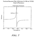
- the reflectance curve has a narrow bandwidth (0.00975 nm), and theoretically reaches 100% reflectivity at the resonant wavelength.
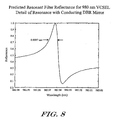
- the reflectance curve still has a narrow bandwidth (0.0097 nm), and theoretically reaches 100% reflectivity at the resonant wavelength. Therefore, and unlike Figure 5, there is little or no degradation in the observed reflectance of the resonant reflector, even when placed adjacent a conductive layer.
- Figure 9 is a schematic cross-sectional side view of a top surface emitting vertical cavity laser similar to that shown in Figure 6, but with a modified grating fill factor.
- the grating fill factor is defined as the grating spacing 102 divided by the grating period 100.
- the resonant wavelength of a resonant reflector is often determined by the grating period 100, and the spectral bandwidth is often determined by the modulation of the refractive index and fill factor of the grating.
- the modulation of the refractive index is related to the difference between the dielectric constants of the grating material and the material that fills the spaces between the grating elements, divided by the average dielectric constant across the grating.
- the average dielectric constant across the grating can be changed by varying the fill factor of the grating. For example, and assuming a constant grating period, the grating fill factor can be increased by reducing the width of each grating element.
- a limitation of achieving a desired spectral bandwidth of a resonant reflector by altering the grating fill factor is that the design rules of many manufacturing processes limit the minimum width of the grating elements. Thus, to achieve some spectral bandwidths, the design rules may have to be pushed, which may reduce the manufacturing yield for the devices.
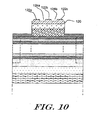
- Figure 10 is a schematic cross-sectional side view of a top surface emitting vertical cavity laser similar to that shown in Figure 6, but with a grating film that has a controlled etch depth to control the spectral bandwidth of the resonant reflector.
- a grating film 120 is provided and subsequently etched to form two or more spaced grating regions 122a-122c separated by one or more spaced etched regions 124a-124b.
- the depth of the etch is controlled. By controlling the depth of the etch, a desired average dielectric constant across the grating can be achieved.
- the grating width and grating spacing may be optimized to the design rules of the manufacturing process, and the etch depth can be controlled to achieve the desired spectral bandwidth. For example, a fill factor of about 50% is preferred. This may increase the producibility and yield of the resonant reflector.
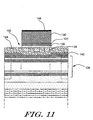
- Figure 11 is a schematic cross-sectional side view of a vertical cavity surface emitting laser that is formed by bonding a resonant reflector 132 that is prepared on a first substrate 130 to a top mirror 134 of a vertical cavity surface emitting laser that is prepared on a second substrate.
- a resonant reflector is formed on a front side 131 of a first substrate 130. This includes forming at least a waveguide 136 and a grating 138, as shown.
- an optoelectronic device such as a vertical cavity surface emitting laser or resonant cavity photodetector, is prepared on a front side of a second substrate.
- this includes a bottom DBR mirror, an active region, a top DBR minor 134, and one or more contacts 140.
- the front side of the first substrate 130 is bonded to the front side of the second substrate to complete the optoelectronic device.
- the first substrate 130 may be bonded to the second substrate using an optical epoxy 144, and preferably a non-conductive optical epoxy.
- the optical epoxy is preferably sufficiently thick, or has a sufficiently low refractive index relative to the refractive index of the waveguide 136 of the resonant reflector 132, so that the energy from the evanescent wave vector in the waveguide 136 is substantially prevented from entering the optoelectronic device on the first substrate.
- a anti-reflective coating 148 may be applied to the backside of the first substrate 130 as shown.
- the relative position of the waveguide 136 and grating 138 may be changed.
- the grating may be positioned more toward the front side of the first substrate than the waveguide.
- the waveguide may be positioned more toward the front side of the first substrate than the grating, if desired.
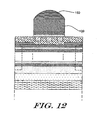
- Figure 12 is a schematic cross-sectional side view of the vertical cavity surface-emitting laser of Figure 11 with a microlens 150 positioned on the backside of the first substrate 130.
- a microlens such as a collimating microlens may be formed on the backside of the first substrate 130.
- a collimating microlens may be formed on the backside of the substrate that carries the bottom mirror, the active region and the top mirror of the optoelectronic device. In either case, the collimating microlens 150 is preferably placed in registration with the output of the optoelectronic device as shown.
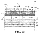
- a number of optoelectronic devices may be formed on a common substrate, as shown in Figure 13.
- One application for such a configuration is a monolithic transceiver that includes one or more light emitting devices 190 and one or more light receiving devices 192 and 194.
- both the light emitting and light receiving devices are formed on a common substrate (not shown).
- a bottom mirror is first formed on the common substrate.
- the bottom mirror may serve as the bottom mirror for more than one of the optoelectronic devices 190, 192 and 194, and is preferably a DBR mirror stack that is doped to be at least partially conductive.
- An active region 200 is then formed on the bottom mirror, followed by a top mirror 202.
- the top mirror 202 is preferably a DBR mirror stack, and is doped to be the opposite conductivity type of the bottom mirror.
- the active region 200 may include cladding layers 204 on either side of the active region 200 to help focus the light energy and current in the active region.
- a deep H+ ion implant may provide gain guide apertures for selected optoelectronic devices, and may further electrically isolate adjacent devices from one another. While a deep H+ implant is provided as an illustration, it is contemplated that any type of current and field confinement may be used, including for example, gain-guided, oxide-confinement, or any other means. Contacts 208a-208d may be provided on the top mirror 202 and on the bottom surface of the common substrate to provide electrical contact to each of the optoelectronic devices.
- a cladding or buffer layer 210 may be provided above the top mirror 202.
- a resonant reflector may then be provided on top of the cladding or buffer layer 210.
- the resonant reflector may include a waveguide 212 and a grating film 214.
- the grating film 214 may be etched to form a grating, as shown.
- the grating may substantially increase the reflectivity of the resonant reflector in those regions.
- the grating film may either include a different grating structure (e.g., wider spectral bandwidth), or remain non-etched as shown.
- the grating film may be removed altogether, and a metal grid 214a-214c may be formed on the waveguide layer 212 or cladding or buffer layer 210, as desired.
- MSM Metal-Semiconductor-Metal
- the cladding or buffer layer 210 may be sufficiently thick to substantially prevent energy in the evanescent tail of the guided mode in the waveguide 212 from entering the top mirror 202.
- the cladding or buffer layer 210 may be formed from a material that has a sufficiently low refractive index relative to the refractive index of the waveguide 212 to substantially prevent energy in the evanescent tail of the guided mode in the waveguide 212 from entering the top mirror 202.
- resonant reflector optoelectronic structures will permit polarization, emission wavelength and mode control. These structures and properties can be designed and fabricated using techniques such as lithography or holography, and may not be subject to growth thickness variations alone. The above techniques can be applied to produce, for example, VCSELs with high power single-mode/polarization emission from apertures exceeding a few microns in diameter. Furthermore, wavelength and/or polarization variation across a chip, array or wafer can be used for spatially varied wavelength/polarization division multiplexing, multi-wavelength spectroscopy, etc.
Landscapes
- Physics & Mathematics (AREA)
- Condensed Matter Physics & Semiconductors (AREA)
- General Physics & Mathematics (AREA)
- Electromagnetism (AREA)
- Optics & Photonics (AREA)
- Semiconductor Lasers (AREA)
- Led Devices (AREA)
- Surface Acoustic Wave Elements And Circuit Networks Thereof (AREA)
- Aerials With Secondary Devices (AREA)
Applications Claiming Priority (3)
| Application Number | Priority Date | Filing Date | Title |
|---|---|---|---|
| US09/751,422 US6782027B2 (en) | 2000-12-29 | 2000-12-29 | Resonant reflector for use with optoelectronic devices |
| US751422 | 2000-12-29 | ||
| PCT/US2001/049089 WO2002060024A2 (en) | 2000-12-29 | 2001-12-18 | Resonant reflector for use with optoelectronic devices |
Publications (2)
| Publication Number | Publication Date |
|---|---|
| EP1362396A2 EP1362396A2 (en) | 2003-11-19 |
| EP1362396B1 true EP1362396B1 (en) | 2006-03-15 |
Family
ID=25021909
Family Applications (1)
| Application Number | Title | Priority Date | Filing Date |
|---|---|---|---|
| EP01994296A Expired - Lifetime EP1362396B1 (en) | 2000-12-29 | 2001-12-18 | Resonant reflector for use with optoelectronic devices |
Country Status (8)
| Country | Link |
|---|---|
| US (2) | US6782027B2 (enExample) |
| EP (1) | EP1362396B1 (enExample) |
| JP (1) | JP2004521491A (enExample) |
| KR (1) | KR20030068573A (enExample) |
| AT (1) | ATE320671T1 (enExample) |
| DE (1) | DE60118035T2 (enExample) |
| TW (1) | TW552750B (enExample) |
| WO (1) | WO2002060024A2 (enExample) |
Families Citing this family (38)
| Publication number | Priority date | Publication date | Assignee | Title |
|---|---|---|---|---|
| US6727520B2 (en) | 2000-12-29 | 2004-04-27 | Honeywell International Inc. | Spatially modulated reflector for an optoelectronic device |
| TWI227799B (en) * | 2000-12-29 | 2005-02-11 | Honeywell Int Inc | Resonant reflector for increased wavelength and polarization control |
| US6813431B2 (en) * | 2002-02-26 | 2004-11-02 | Intel Corporation | Integrated photodevice and waveguide |
| JP4074498B2 (ja) * | 2002-09-25 | 2008-04-09 | セイコーエプソン株式会社 | 面発光型発光素子、光モジュールおよび光伝達装置 |
| US7299991B2 (en) * | 2003-04-08 | 2007-11-27 | Avago Technologies Ecbu Ip (Singapore) Pte. Ltd. | Reflective members for use in encoder systems |
| TW200505120A (en) * | 2003-07-29 | 2005-02-01 | Copax Photonics Corp | Single transverse mode vertical cavity surface emitting laser device with array structure and method for fabricating the same |
| US7269196B2 (en) * | 2004-07-06 | 2007-09-11 | Avago Technologies Fiber Ip (Singapore) Pte. Ltd. | Method for increasing maximum modulation speed of a light emitting device, and light emitting device with increased maximum modulation speed and quantum well structure thereof |
| US7920612B2 (en) * | 2004-08-31 | 2011-04-05 | Finisar Corporation | Light emitting semiconductor device having an electrical confinement barrier near the active region |
| US7596165B2 (en) * | 2004-08-31 | 2009-09-29 | Finisar Corporation | Distributed Bragg Reflector for optoelectronic device |
| US7829912B2 (en) * | 2006-07-31 | 2010-11-09 | Finisar Corporation | Efficient carrier injection in a semiconductor device |
| US7385691B2 (en) * | 2005-01-27 | 2008-06-10 | Hewlett-Packard Development Company, L.P. | Integrated modular system and method for enhanced Raman spectroscopy |
| US7151599B2 (en) * | 2005-01-27 | 2006-12-19 | Hewlett-Packard Development Company, L.P. | Monolithic system and method for enhanced Raman spectroscopy |
| US7136160B2 (en) * | 2005-01-27 | 2006-11-14 | Hewlett-Packard Development Company, L.P. | Integrated system and method for transversal enhanced Raman Spectroscopy |
| JP4515949B2 (ja) * | 2005-03-31 | 2010-08-04 | 株式会社東芝 | 面型光半導体素子 |
| US7629661B2 (en) * | 2006-02-10 | 2009-12-08 | Noble Peak Vision Corp. | Semiconductor devices with photoresponsive components and metal silicide light blocking structures |
| JP2007234824A (ja) * | 2006-02-28 | 2007-09-13 | Canon Inc | 垂直共振器型面発光レーザ |
| US7805826B1 (en) * | 2006-07-06 | 2010-10-05 | Hewlett-Packard Development Company, L.P. | Fabrication of slot waveguide |
| US7627017B2 (en) * | 2006-08-25 | 2009-12-01 | Stc. Unm | Laser amplifier and method of making the same |
| CN101535859B (zh) * | 2006-09-13 | 2012-05-02 | 埃迪斯科文大学 | 光学连接组件 |
| US8031752B1 (en) | 2007-04-16 | 2011-10-04 | Finisar Corporation | VCSEL optimized for high speed data |
| JP5300344B2 (ja) * | 2007-07-06 | 2013-09-25 | キヤノン株式会社 | 光検出素子及び撮像素子、光検出方法及び撮像方法 |
| JP4911774B2 (ja) * | 2007-07-25 | 2012-04-04 | パナソニック株式会社 | 光送受信装置及びそれを用いた光通信システム |
| JP2009158955A (ja) * | 2007-12-06 | 2009-07-16 | Rohm Co Ltd | 窒化物半導体レーザダイオード |
| US8617993B2 (en) * | 2010-02-01 | 2013-12-31 | Lam Research Corporation | Method of reducing pattern collapse in high aspect ratio nanostructures |
| US8646949B2 (en) * | 2010-03-03 | 2014-02-11 | LumenFlow Corp. | Constrained folded path resonant white light scintillator |
| WO2013105959A1 (en) * | 2012-01-12 | 2013-07-18 | Hewlett-Packard Development Company, L.P. | Integrated sub-wavelength grating system |
| CN103999304A (zh) * | 2012-01-18 | 2014-08-20 | 惠普发展公司,有限责任合伙企业 | 集成亚波长光栅元件 |
| KR20130085763A (ko) * | 2012-01-20 | 2013-07-30 | 삼성전자주식회사 | 광 집적 회로용 혼성 레이저 광원 |
| TW201504599A (zh) * | 2013-05-30 | 2015-02-01 | Univ California | 具有高對比光柵及可作爲雙重用途之高對比光柵垂直腔表面發射雷射檢測器之二維週期結構的極化無關光檢測器 |
| US10826274B2 (en) | 2018-02-12 | 2020-11-03 | Lumentum Operations Llc | Grating structure for surface-emitting laser |
| WO2020014561A1 (en) * | 2018-07-13 | 2020-01-16 | The Government of the United State of America, as represented by the Secretary of the Navy | Highly stable semiconductor lasers and sensors for iii-v and silicon photonic integrated circuits |
| US10818807B2 (en) * | 2019-01-21 | 2020-10-27 | Globalfoundries Inc. | Semiconductor detectors integrated with Bragg reflectors |
| US11437785B2 (en) * | 2019-09-23 | 2022-09-06 | Taiwan Semiconductor Manufacturing Company, Ltd. | VCSEL with self-aligned microlens to improve beam divergence |
| CN110676689A (zh) * | 2019-10-12 | 2020-01-10 | 长春理工大学 | 一种垂直腔面发射半导体激光器及其制备方法 |
| US11340403B2 (en) * | 2020-03-03 | 2022-05-24 | Globalfoundries U.S. Inc. | Photonic component with distributed Bragg reflectors |
| US12149049B2 (en) * | 2020-12-31 | 2024-11-19 | Win Semiconductors Corp. | Vertical-cavity surface-emitting laser and method for forming the same |
| US20240186766A1 (en) * | 2022-10-19 | 2024-06-06 | Ii-Vi Delaware, Inc. | Polarized/lensed back-side emitting (bse) vertical-cavity surface-emitting laser (vcsel) |
| CN120821012B (zh) * | 2025-09-17 | 2025-12-02 | 北京阿法龙科技有限公司 | 基于纳米压印的超表面光栅结构、其制造方法及系统 |
Family Cites Families (63)
| Publication number | Priority date | Publication date | Assignee | Title |
|---|---|---|---|---|
| CA1108902A (en) | 1978-06-15 | 1981-09-15 | R. Ian Macdonald | Wavelength selective optical coupler |
| US4317085A (en) | 1979-09-12 | 1982-02-23 | Xerox Corporation | Channeled mesa laser |
| JPS60123084A (ja) | 1983-12-08 | 1985-07-01 | Matsushita Electric Ind Co Ltd | 半導体光発生装置 |
| US4660207A (en) | 1984-11-21 | 1987-04-21 | Northern Telecom Limited | Surface-emitting light emitting device |
| US4784722A (en) | 1985-01-22 | 1988-11-15 | Massachusetts Institute Of Technology | Method forming surface emitting diode laser |
| GB2203891A (en) | 1987-04-21 | 1988-10-26 | Plessey Co Plc | Semiconductor diode laser array |
| JPS63318195A (ja) | 1987-06-19 | 1988-12-27 | Agency Of Ind Science & Technol | 横方向埋め込み型面発光レ−ザ |
| US4885592A (en) | 1987-12-28 | 1989-12-05 | Kofol J Stephen | Electronically steerable antenna |
| US4904045A (en) * | 1988-03-25 | 1990-02-27 | American Telephone And Telegraph Company | Grating coupler with monolithically integrated quantum well index modulator |
| JPH0254981A (ja) | 1988-08-20 | 1990-02-23 | Fujitsu Ltd | 面発光レーザ及びレーザアレイ |
| US4901327A (en) | 1988-10-24 | 1990-02-13 | General Dynamics Corporation, Electronics Division | Transverse injection surface emitting laser |
| US4943970A (en) | 1988-10-24 | 1990-07-24 | General Dynamics Corporation, Electronics Division | Surface emitting laser |
| US4956844A (en) | 1989-03-17 | 1990-09-11 | Massachusetts Institute Of Technology | Two-dimensional surface-emitting laser array |
| US5031187A (en) | 1990-02-14 | 1991-07-09 | Bell Communications Research, Inc. | Planar array of vertical-cavity, surface-emitting lasers |
| US5204871A (en) | 1990-03-29 | 1993-04-20 | Larkins Eric C | Bistable optical laser based on a heterostructure pnpn thyristor |
| US5115442A (en) | 1990-04-13 | 1992-05-19 | At&T Bell Laboratories | Top-emitting surface emitting laser structures |
| US5034958A (en) | 1990-04-19 | 1991-07-23 | Bell Communications Research, Inc. | Front-surface emitting diode laser |
| US5052016A (en) | 1990-05-18 | 1991-09-24 | University Of New Mexico | Resonant-periodic-gain distributed-feedback surface-emitting semiconductor laser |
| US5056098A (en) | 1990-07-05 | 1991-10-08 | At&T Bell Laboratories | Vertical cavity laser with mirror having controllable reflectivity |
| US5158908A (en) | 1990-08-31 | 1992-10-27 | At&T Bell Laboratories | Distributed bragg reflectors and devices incorporating same |
| US5237581A (en) | 1990-11-14 | 1993-08-17 | Nec Corporation | Semiconductor multilayer reflector and light emitting device with the same |
| US5216263A (en) | 1990-11-29 | 1993-06-01 | Xerox Corporation | High density, independently addressable, surface emitting semiconductor laser-light emitting diode arrays |
| US5062115A (en) | 1990-12-28 | 1991-10-29 | Xerox Corporation | High density, independently addressable, surface emitting semiconductor laser/light emitting diode arrays |
| US5140605A (en) | 1991-06-27 | 1992-08-18 | Xerox Corporation | Thermally stabilized diode laser structure |
| US5216680A (en) | 1991-07-11 | 1993-06-01 | Board Of Regents, The University Of Texas System | Optical guided-mode resonance filter |
| US5258990A (en) | 1991-11-07 | 1993-11-02 | The United States Of America As Represented By The Secretary Of The United States Department Of Energy | Visible light surface emitting semiconductor laser |
| US5404373A (en) | 1991-11-08 | 1995-04-04 | University Of New Mexico | Electro-optical device |
| US5325386A (en) | 1992-04-21 | 1994-06-28 | Bandgap Technology Corporation | Vertical-cavity surface emitting laser assay display system |
| JP3206097B2 (ja) | 1992-04-22 | 2001-09-04 | セイコーエプソン株式会社 | 面発光型半導体レーザ |
| US5245622A (en) | 1992-05-07 | 1993-09-14 | Bandgap Technology Corporation | Vertical-cavity surface-emitting lasers with intra-cavity structures |
| US5285466A (en) | 1992-05-20 | 1994-02-08 | Wisconsin Alumni Research Foundation | Feedback mechanism for vertical cavity surface emitting lasers |
| US5293392A (en) | 1992-07-31 | 1994-03-08 | Motorola, Inc. | Top emitting VCSEL with etch stop layer |
| US5317587A (en) | 1992-08-06 | 1994-05-31 | Motorola, Inc. | VCSEL with separate control of current distribution and optical mode |
| JPH0669585A (ja) | 1992-08-12 | 1994-03-11 | Fujitsu Ltd | 面発光半導体レーザ及びその製造方法 |
| US5363397A (en) | 1992-10-29 | 1994-11-08 | Internatioal Business Machines Corporation | Integrated short cavity laser with bragg mirrors |
| US5428634A (en) | 1992-11-05 | 1995-06-27 | The United States Of America As Represented By The United States Department Of Energy | Visible light emitting vertical cavity surface emitting lasers |
| DE4240706A1 (de) | 1992-12-03 | 1994-06-09 | Siemens Ag | Oberflächenemittierende Laserdiode |
| US5331654A (en) | 1993-03-05 | 1994-07-19 | Photonics Research Incorporated | Polarized surface-emitting laser |
| US5416044A (en) | 1993-03-12 | 1995-05-16 | Matsushita Electric Industrial Co., Ltd. | Method for producing a surface-emitting laser |
| US5351256A (en) | 1993-04-28 | 1994-09-27 | The United States Of America As Represented By The United States Department Of Energy | Electrically injected visible vertical cavity surface emitting laser diodes |
| US5359618A (en) | 1993-06-01 | 1994-10-25 | Motorola, Inc. | High efficiency VCSEL and method of fabrication |
| US5359447A (en) | 1993-06-25 | 1994-10-25 | Hewlett-Packard Company | Optical communication with vertical-cavity surface-emitting laser operating in multiple transverse modes |
| US5446754A (en) | 1993-11-05 | 1995-08-29 | Photonics Research Incorporated | Phased array semiconductor laser |
| US5475701A (en) | 1993-12-29 | 1995-12-12 | Honeywell Inc. | Integrated laser power monitor |
| KR0132018B1 (ko) | 1994-01-27 | 1998-04-14 | 김만제 | 세원형 그레이팅 표면 방출형 레이저 다이오드 |
| US5513202A (en) | 1994-02-25 | 1996-04-30 | Matsushita Electric Industrial Co., Ltd. | Vertical-cavity surface-emitting semiconductor laser |
| US5606572A (en) | 1994-03-24 | 1997-02-25 | Vixel Corporation | Integration of laser with photodiode for feedback control |
| US6064783A (en) * | 1994-05-25 | 2000-05-16 | Congdon; Philip A. | Integrated laser and coupled waveguide |
| US5557626A (en) | 1994-06-15 | 1996-09-17 | Motorola | Patterned mirror VCSEL with adjustable selective etch region |
| US5778018A (en) | 1994-10-13 | 1998-07-07 | Nec Corporation | VCSELs (vertical-cavity surface emitting lasers) and VCSEL-based devices |
| US5530715A (en) | 1994-11-29 | 1996-06-25 | Motorola, Inc. | Vertical cavity surface emitting laser having continuous grading |
| US5568499A (en) | 1995-04-07 | 1996-10-22 | Sandia Corporation | Optical device with low electrical and thermal resistance bragg reflectors |
| US5598300A (en) | 1995-06-05 | 1997-01-28 | Board Of Regents, The University Of Texas System | Efficient bandpass reflection and transmission filters with low sidebands based on guided-mode resonance effects |
| US5978401A (en) | 1995-10-25 | 1999-11-02 | Honeywell Inc. | Monolithic vertical cavity surface emitting laser and resonant cavity photodetector transceiver |
| US5727013A (en) | 1995-10-27 | 1998-03-10 | Wisconsin Alumni Research Foundation | Single lobe surface emitting complex coupled distributed feedback semiconductor laser |
| FR2741483B1 (fr) | 1995-11-21 | 1998-01-02 | Thomson Csf | Dispositif optoelectronique a puits quantiques |
| US5903590A (en) | 1996-05-20 | 1999-05-11 | Sandia Corporation | Vertical-cavity surface-emitting laser device |
| US5940422A (en) | 1996-06-28 | 1999-08-17 | Honeywell Inc. | Laser with an improved mode control |
| US5774487A (en) | 1996-10-16 | 1998-06-30 | Honeywell Inc. | Filamented multi-wavelength vertical-cavity surface emitting laser |
| US5835521A (en) * | 1997-02-10 | 1998-11-10 | Motorola, Inc. | Long wavelength light emitting vertical cavity surface emitting laser and method of fabrication |
| US6055262A (en) * | 1997-06-11 | 2000-04-25 | Honeywell Inc. | Resonant reflector for improved optoelectronic device performance and enhanced applicability |
| US6064683A (en) | 1997-12-12 | 2000-05-16 | Honeywell Inc. | Bandgap isolated light emitter |
| US6330388B1 (en) * | 1999-01-27 | 2001-12-11 | Northstar Photonics, Inc. | Method and apparatus for waveguide optics and devices |
-
2000
- 2000-12-29 US US09/751,422 patent/US6782027B2/en not_active Expired - Lifetime
-
2001
- 2001-12-18 JP JP2002560248A patent/JP2004521491A/ja active Pending
- 2001-12-18 AT AT01994296T patent/ATE320671T1/de not_active IP Right Cessation
- 2001-12-18 WO PCT/US2001/049089 patent/WO2002060024A2/en not_active Ceased
- 2001-12-18 EP EP01994296A patent/EP1362396B1/en not_active Expired - Lifetime
- 2001-12-18 DE DE60118035T patent/DE60118035T2/de not_active Expired - Lifetime
- 2001-12-18 KR KR10-2003-7008907A patent/KR20030068573A/ko not_active Ceased
- 2001-12-28 TW TW090132816A patent/TW552750B/zh not_active IP Right Cessation
-
2004
- 2004-07-06 US US10/884,895 patent/US7288421B2/en not_active Expired - Fee Related
Also Published As
| Publication number | Publication date |
|---|---|
| KR20030068573A (ko) | 2003-08-21 |
| US20040248331A1 (en) | 2004-12-09 |
| JP2004521491A (ja) | 2004-07-15 |
| US20030103542A1 (en) | 2003-06-05 |
| ATE320671T1 (de) | 2006-04-15 |
| EP1362396A2 (en) | 2003-11-19 |
| HK1061609A1 (en) | 2004-09-24 |
| US7288421B2 (en) | 2007-10-30 |
| TW552750B (en) | 2003-09-11 |
| DE60118035D1 (de) | 2006-05-11 |
| US6782027B2 (en) | 2004-08-24 |
| WO2002060024A2 (en) | 2002-08-01 |
| WO2002060024A3 (en) | 2003-01-16 |
| DE60118035T2 (de) | 2006-11-16 |
Similar Documents
| Publication | Publication Date | Title |
|---|---|---|
| EP1362396B1 (en) | Resonant reflector for use with optoelectronic devices | |
| US6836501B2 (en) | Resonant reflector for increased wavelength and polarization control | |
| US6055262A (en) | Resonant reflector for improved optoelectronic device performance and enhanced applicability | |
| US6148016A (en) | Integrated semiconductor lasers and photodetectors | |
| EP1352455B1 (en) | Spatially modulated reflector for an optoelectronic device | |
| US5978401A (en) | Monolithic vertical cavity surface emitting laser and resonant cavity photodetector transceiver | |
| EP1208622B1 (en) | Coupled cavity anti-guided vertical cavity surface emitting laser (vcsel) | |
| US5903590A (en) | Vertical-cavity surface-emitting laser device | |
| US8189642B1 (en) | VCSEL semiconductor device | |
| US6611544B1 (en) | Method and apparatus for narrow bandwidth distributed bragg reflector semiconductor lasers | |
| US20050063440A1 (en) | Epitaxial mode-confined vertical cavity surface emitting laser (VCSEL) and method of manufacturing same | |
| CA2622301A1 (en) | Optical phase conjugation laser diode | |
| US8599897B2 (en) | Tunable detector | |
| US20050100063A1 (en) | Mirror structure for reducing the effect of feedback on a VCSEL | |
| US7596165B2 (en) | Distributed Bragg Reflector for optoelectronic device | |
| US7126750B2 (en) | Folded cavity semiconductor optical amplifier (FCSOA) | |
| US20050018729A1 (en) | Implant damaged oxide insulating region in vertical cavity surface emitting laser | |
| HK1061609B (en) | Resonant reflector for use with optoelectronic devices | |
| JP2006514431A (ja) | 面発光型半導体レーザの導波路構造の製造方法及び面発光型半導体レーザ |
Legal Events
| Date | Code | Title | Description |
|---|---|---|---|
| PUAI | Public reference made under article 153(3) epc to a published international application that has entered the european phase |
Free format text: ORIGINAL CODE: 0009012 |
|
| 17P | Request for examination filed |
Effective date: 20030701 |
|
| AK | Designated contracting states |
Kind code of ref document: A2 Designated state(s): AT BE CH CY DE DK ES FI FR GB GR IE IT LI LU MC NL PT SE TR |
|
| AX | Request for extension of the european patent |
Extension state: AL LT LV MK RO SI |
|
| REG | Reference to a national code |
Ref country code: HK Ref legal event code: DE Ref document number: 1061609 Country of ref document: HK |
|
| 17Q | First examination report despatched |
Effective date: 20040826 |
|
| RAP1 | Party data changed (applicant data changed or rights of an application transferred) |
Owner name: FINISAR CORPORATION |
|
| GRAP | Despatch of communication of intention to grant a patent |
Free format text: ORIGINAL CODE: EPIDOSNIGR1 |
|
| GRAS | Grant fee paid |
Free format text: ORIGINAL CODE: EPIDOSNIGR3 |
|
| GRAA | (expected) grant |
Free format text: ORIGINAL CODE: 0009210 |
|
| AK | Designated contracting states |
Kind code of ref document: B1 Designated state(s): AT BE CH CY DE DK ES FI FR GB GR IE IT LI LU MC NL PT SE TR |
|
| PG25 | Lapsed in a contracting state [announced via postgrant information from national office to epo] |
Ref country code: AT Free format text: LAPSE BECAUSE OF FAILURE TO SUBMIT A TRANSLATION OF THE DESCRIPTION OR TO PAY THE FEE WITHIN THE PRESCRIBED TIME-LIMIT Effective date: 20060315 Ref country code: BE Free format text: LAPSE BECAUSE OF FAILURE TO SUBMIT A TRANSLATION OF THE DESCRIPTION OR TO PAY THE FEE WITHIN THE PRESCRIBED TIME-LIMIT Effective date: 20060315 Ref country code: LI Free format text: LAPSE BECAUSE OF FAILURE TO SUBMIT A TRANSLATION OF THE DESCRIPTION OR TO PAY THE FEE WITHIN THE PRESCRIBED TIME-LIMIT Effective date: 20060315 Ref country code: CH Free format text: LAPSE BECAUSE OF FAILURE TO SUBMIT A TRANSLATION OF THE DESCRIPTION OR TO PAY THE FEE WITHIN THE PRESCRIBED TIME-LIMIT Effective date: 20060315 Ref country code: FI Free format text: LAPSE BECAUSE OF FAILURE TO SUBMIT A TRANSLATION OF THE DESCRIPTION OR TO PAY THE FEE WITHIN THE PRESCRIBED TIME-LIMIT Effective date: 20060315 Ref country code: NL Free format text: LAPSE BECAUSE OF FAILURE TO SUBMIT A TRANSLATION OF THE DESCRIPTION OR TO PAY THE FEE WITHIN THE PRESCRIBED TIME-LIMIT Effective date: 20060315 Ref country code: IT Free format text: LAPSE BECAUSE OF FAILURE TO SUBMIT A TRANSLATION OF THE DESCRIPTION OR TO PAY THE FEE WITHIN THE PRESCRIBED TIME-LIMIT;WARNING: LAPSES OF ITALIAN PATENTS WITH EFFECTIVE DATE BEFORE 2007 MAY HAVE OCCURRED AT ANY TIME BEFORE 2007. THE CORRECT EFFECTIVE DATE MAY BE DIFFERENT FROM THE ONE RECORDED. Effective date: 20060315 |
|
| REG | Reference to a national code |
Ref country code: GB Ref legal event code: FG4D Ref country code: CH Ref legal event code: EP |
|
| REG | Reference to a national code |
Ref country code: IE Ref legal event code: FG4D |
|
| REF | Corresponds to: |
Ref document number: 60118035 Country of ref document: DE Date of ref document: 20060511 Kind code of ref document: P |
|
| PG25 | Lapsed in a contracting state [announced via postgrant information from national office to epo] |
Ref country code: DK Free format text: LAPSE BECAUSE OF FAILURE TO SUBMIT A TRANSLATION OF THE DESCRIPTION OR TO PAY THE FEE WITHIN THE PRESCRIBED TIME-LIMIT Effective date: 20060615 Ref country code: SE Free format text: LAPSE BECAUSE OF FAILURE TO SUBMIT A TRANSLATION OF THE DESCRIPTION OR TO PAY THE FEE WITHIN THE PRESCRIBED TIME-LIMIT Effective date: 20060615 |
|
| PG25 | Lapsed in a contracting state [announced via postgrant information from national office to epo] |
Ref country code: ES Free format text: LAPSE BECAUSE OF FAILURE TO SUBMIT A TRANSLATION OF THE DESCRIPTION OR TO PAY THE FEE WITHIN THE PRESCRIBED TIME-LIMIT Effective date: 20060626 |
|
| PG25 | Lapsed in a contracting state [announced via postgrant information from national office to epo] |
Ref country code: PT Free format text: LAPSE BECAUSE OF FAILURE TO SUBMIT A TRANSLATION OF THE DESCRIPTION OR TO PAY THE FEE WITHIN THE PRESCRIBED TIME-LIMIT Effective date: 20060816 |
|
| NLV1 | Nl: lapsed or annulled due to failure to fulfill the requirements of art. 29p and 29m of the patents act | ||
| REG | Reference to a national code |
Ref country code: HK Ref legal event code: GR Ref document number: 1061609 Country of ref document: HK |
|
| ET | Fr: translation filed | ||
| REG | Reference to a national code |
Ref country code: CH Ref legal event code: PL |
|
| PG25 | Lapsed in a contracting state [announced via postgrant information from national office to epo] |
Ref country code: IE Free format text: LAPSE BECAUSE OF NON-PAYMENT OF DUE FEES Effective date: 20061218 |
|
| PG25 | Lapsed in a contracting state [announced via postgrant information from national office to epo] |
Ref country code: MC Free format text: LAPSE BECAUSE OF NON-PAYMENT OF DUE FEES Effective date: 20061231 |
|
| PLBE | No opposition filed within time limit |
Free format text: ORIGINAL CODE: 0009261 |
|
| STAA | Information on the status of an ep patent application or granted ep patent |
Free format text: STATUS: NO OPPOSITION FILED WITHIN TIME LIMIT |
|
| 26N | No opposition filed |
Effective date: 20061218 |
|
| PG25 | Lapsed in a contracting state [announced via postgrant information from national office to epo] |
Ref country code: GR Free format text: LAPSE BECAUSE OF FAILURE TO SUBMIT A TRANSLATION OF THE DESCRIPTION OR TO PAY THE FEE WITHIN THE PRESCRIBED TIME-LIMIT Effective date: 20060616 |
|
| PG25 | Lapsed in a contracting state [announced via postgrant information from national office to epo] |
Ref country code: TR Free format text: LAPSE BECAUSE OF FAILURE TO SUBMIT A TRANSLATION OF THE DESCRIPTION OR TO PAY THE FEE WITHIN THE PRESCRIBED TIME-LIMIT Effective date: 20060315 Ref country code: LU Free format text: LAPSE BECAUSE OF NON-PAYMENT OF DUE FEES Effective date: 20061218 |
|
| PG25 | Lapsed in a contracting state [announced via postgrant information from national office to epo] |
Ref country code: CY Free format text: LAPSE BECAUSE OF FAILURE TO SUBMIT A TRANSLATION OF THE DESCRIPTION OR TO PAY THE FEE WITHIN THE PRESCRIBED TIME-LIMIT Effective date: 20060315 |
|
| PGFP | Annual fee paid to national office [announced via postgrant information from national office to epo] |
Ref country code: GB Payment date: 20141229 Year of fee payment: 14 |
|
| PGFP | Annual fee paid to national office [announced via postgrant information from national office to epo] |
Ref country code: FR Payment date: 20141217 Year of fee payment: 14 |
|
| PGFP | Annual fee paid to national office [announced via postgrant information from national office to epo] |
Ref country code: DE Payment date: 20141230 Year of fee payment: 14 |
|
| REG | Reference to a national code |
Ref country code: DE Ref legal event code: R119 Ref document number: 60118035 Country of ref document: DE |
|
| GBPC | Gb: european patent ceased through non-payment of renewal fee |
Effective date: 20151218 |
|
| REG | Reference to a national code |
Ref country code: FR Ref legal event code: ST Effective date: 20160831 |
|
| PG25 | Lapsed in a contracting state [announced via postgrant information from national office to epo] |
Ref country code: DE Free format text: LAPSE BECAUSE OF NON-PAYMENT OF DUE FEES Effective date: 20160701 Ref country code: GB Free format text: LAPSE BECAUSE OF NON-PAYMENT OF DUE FEES Effective date: 20151218 |
|
| PG25 | Lapsed in a contracting state [announced via postgrant information from national office to epo] |
Ref country code: FR Free format text: LAPSE BECAUSE OF NON-PAYMENT OF DUE FEES Effective date: 20151231 |