EP1360548B1 - Electrooptical displays with multilayer structure achieved by varying rates of polymerization - Google Patents
Electrooptical displays with multilayer structure achieved by varying rates of polymerization Download PDFInfo
- Publication number
- EP1360548B1 EP1360548B1 EP02723135A EP02723135A EP1360548B1 EP 1360548 B1 EP1360548 B1 EP 1360548B1 EP 02723135 A EP02723135 A EP 02723135A EP 02723135 A EP02723135 A EP 02723135A EP 1360548 B1 EP1360548 B1 EP 1360548B1
- Authority
- EP
- European Patent Office
- Prior art keywords
- polymer
- polymerization
- liquid crystal
- spacers
- substrates
- Prior art date
- Legal status (The legal status is an assumption and is not a legal conclusion. Google has not performed a legal analysis and makes no representation as to the accuracy of the status listed.)
- Expired - Lifetime
Links
Images


Classifications
-
- G—PHYSICS
- G02—OPTICS
- G02F—OPTICAL DEVICES OR ARRANGEMENTS FOR THE CONTROL OF LIGHT BY MODIFICATION OF THE OPTICAL PROPERTIES OF THE MEDIA OF THE ELEMENTS INVOLVED THEREIN; NON-LINEAR OPTICS; FREQUENCY-CHANGING OF LIGHT; OPTICAL LOGIC ELEMENTS; OPTICAL ANALOGUE/DIGITAL CONVERTERS
- G02F1/00—Devices or arrangements for the control of the intensity, colour, phase, polarisation or direction of light arriving from an independent light source, e.g. switching, gating or modulating; Non-linear optics
- G02F1/01—Devices or arrangements for the control of the intensity, colour, phase, polarisation or direction of light arriving from an independent light source, e.g. switching, gating or modulating; Non-linear optics for the control of the intensity, phase, polarisation or colour
- G02F1/13—Devices or arrangements for the control of the intensity, colour, phase, polarisation or direction of light arriving from an independent light source, e.g. switching, gating or modulating; Non-linear optics for the control of the intensity, phase, polarisation or colour based on liquid crystals, e.g. single liquid crystal display cells
- G02F1/133—Constructional arrangements; Operation of liquid crystal cells; Circuit arrangements
- G02F1/1333—Constructional arrangements; Manufacturing methods
- G02F1/1334—Constructional arrangements; Manufacturing methods based on polymer dispersed liquid crystals, e.g. microencapsulated liquid crystals
-
- G—PHYSICS
- G02—OPTICS
- G02F—OPTICAL DEVICES OR ARRANGEMENTS FOR THE CONTROL OF LIGHT BY MODIFICATION OF THE OPTICAL PROPERTIES OF THE MEDIA OF THE ELEMENTS INVOLVED THEREIN; NON-LINEAR OPTICS; FREQUENCY-CHANGING OF LIGHT; OPTICAL LOGIC ELEMENTS; OPTICAL ANALOGUE/DIGITAL CONVERTERS
- G02F1/00—Devices or arrangements for the control of the intensity, colour, phase, polarisation or direction of light arriving from an independent light source, e.g. switching, gating or modulating; Non-linear optics
- G02F1/01—Devices or arrangements for the control of the intensity, colour, phase, polarisation or direction of light arriving from an independent light source, e.g. switching, gating or modulating; Non-linear optics for the control of the intensity, phase, polarisation or colour
- G02F1/13—Devices or arrangements for the control of the intensity, colour, phase, polarisation or direction of light arriving from an independent light source, e.g. switching, gating or modulating; Non-linear optics for the control of the intensity, phase, polarisation or colour based on liquid crystals, e.g. single liquid crystal display cells
-
- G—PHYSICS
- G02—OPTICS
- G02F—OPTICAL DEVICES OR ARRANGEMENTS FOR THE CONTROL OF LIGHT BY MODIFICATION OF THE OPTICAL PROPERTIES OF THE MEDIA OF THE ELEMENTS INVOLVED THEREIN; NON-LINEAR OPTICS; FREQUENCY-CHANGING OF LIGHT; OPTICAL LOGIC ELEMENTS; OPTICAL ANALOGUE/DIGITAL CONVERTERS
- G02F1/00—Devices or arrangements for the control of the intensity, colour, phase, polarisation or direction of light arriving from an independent light source, e.g. switching, gating or modulating; Non-linear optics
- G02F1/01—Devices or arrangements for the control of the intensity, colour, phase, polarisation or direction of light arriving from an independent light source, e.g. switching, gating or modulating; Non-linear optics for the control of the intensity, phase, polarisation or colour
- G02F1/13—Devices or arrangements for the control of the intensity, colour, phase, polarisation or direction of light arriving from an independent light source, e.g. switching, gating or modulating; Non-linear optics for the control of the intensity, phase, polarisation or colour based on liquid crystals, e.g. single liquid crystal display cells
- G02F1/133—Constructional arrangements; Operation of liquid crystal cells; Circuit arrangements
- G02F1/1333—Constructional arrangements; Manufacturing methods
- G02F1/1339—Gaskets; Spacers; Sealing of cells
- G02F1/13394—Gaskets; Spacers; Sealing of cells spacers regularly patterned on the cell subtrate, e.g. walls, pillars
-
- G—PHYSICS
- G02—OPTICS
- G02F—OPTICAL DEVICES OR ARRANGEMENTS FOR THE CONTROL OF LIGHT BY MODIFICATION OF THE OPTICAL PROPERTIES OF THE MEDIA OF THE ELEMENTS INVOLVED THEREIN; NON-LINEAR OPTICS; FREQUENCY-CHANGING OF LIGHT; OPTICAL LOGIC ELEMENTS; OPTICAL ANALOGUE/DIGITAL CONVERTERS
- G02F1/00—Devices or arrangements for the control of the intensity, colour, phase, polarisation or direction of light arriving from an independent light source, e.g. switching, gating or modulating; Non-linear optics
- G02F1/01—Devices or arrangements for the control of the intensity, colour, phase, polarisation or direction of light arriving from an independent light source, e.g. switching, gating or modulating; Non-linear optics for the control of the intensity, phase, polarisation or colour
- G02F1/13—Devices or arrangements for the control of the intensity, colour, phase, polarisation or direction of light arriving from an independent light source, e.g. switching, gating or modulating; Non-linear optics for the control of the intensity, phase, polarisation or colour based on liquid crystals, e.g. single liquid crystal display cells
- G02F1/137—Devices or arrangements for the control of the intensity, colour, phase, polarisation or direction of light arriving from an independent light source, e.g. switching, gating or modulating; Non-linear optics for the control of the intensity, phase, polarisation or colour based on liquid crystals, e.g. single liquid crystal display cells characterised by the electro-optical or magneto-optical effect, e.g. field-induced phase transition, orientation effect, guest-host interaction or dynamic scattering
- G02F1/139—Devices or arrangements for the control of the intensity, colour, phase, polarisation or direction of light arriving from an independent light source, e.g. switching, gating or modulating; Non-linear optics for the control of the intensity, phase, polarisation or colour based on liquid crystals, e.g. single liquid crystal display cells characterised by the electro-optical or magneto-optical effect, e.g. field-induced phase transition, orientation effect, guest-host interaction or dynamic scattering based on orientation effects in which the liquid crystal remains transparent
- G02F1/141—Devices or arrangements for the control of the intensity, colour, phase, polarisation or direction of light arriving from an independent light source, e.g. switching, gating or modulating; Non-linear optics for the control of the intensity, phase, polarisation or colour based on liquid crystals, e.g. single liquid crystal display cells characterised by the electro-optical or magneto-optical effect, e.g. field-induced phase transition, orientation effect, guest-host interaction or dynamic scattering based on orientation effects in which the liquid crystal remains transparent using ferroelectric liquid crystals
Definitions
- This invention relates to liquid crystal and other electronic displays.
- an electronic display it is highly desirable for an electronic display to be as thin and light as possible while still maintaining a high degree of ruggedness and protection against forces caused by shock, pressure, flexure, and dropping, among other things.
- size and weight are critical factors to the commercial success of a product, but currently breakage of the displays within these devices is one of the primary reasons for repairs and product returns.
- Electrophoretic displays achieve images via electrophoretics--the rapid migration of microparticles in colloidal suspensions.
- Light scattering particles are moved within a dyed colloidal suspension by electrostatic forces. The particles will either move toward the viewer, in which case, the typically white particles are seen by the viewer, or to the surface away from the viewer, in which case, the white particles will be hidden by the dark dye.
- Cholesteric displays are another display technology being attempted on plastic substrates.
- cholesteric liquid-crystal material can be switched between two stable states--the so-called focal conic and planar states--in which the liquid crystal's helical structures have different orientations.
- focal conic state the helical structures are unaligned and the liquid crystal is transparent.
- planar state the helical structures' axes are all perpendicular to the display's surface resulting in essentially monochromatic transmission by the display.
- the Gyricon display being developed by Xerox, is made of microscopic beads, randomly dispersed and held in place between two plastic sheets by a flexible elastomeric matrix of oil-filled cavities.
- the balls have strongly contrasting hemispheres, black on one side and white on the other.
- the white side is highly reflective, while the black side absorbs light.
- Each hemisphere has a unique intrinsic charge, resulting in a force on the ball when an electric field is applied and the axis of the ball is not aligned with the field.
- the side of the ball presented for display depends on the polarity of the voltage applied to the electrode. In all three of these cases, while they have some positive features such as high contrast and compatibility with plastic substrates, they all currently require high drive voltages, have slow response times, and are not compatible with commercially available drive electronics.
- LCDs Liquid crystal displays
- PDLCDs polymer dispersed displays
- Patents Nos. 5,473,450 and 5,333,074 describe methods of localizing the polymer during photopolymerization by exposing only portions of the device to the light source using masks. Polymer structures of a size on the order of a pixel ( ⁇ 0.3 mm) are achievable, but manufacturing may be more difficult since the photomask must generally be aligned to the electrode structure within the device, and expensive collimated UV light sources must generally be employed. Structures much smaller than 0.3 mm may be difficult to achieve due to the inherent scattering of the LC/polymer mixture.
- U.S. Patent No. 5,473,450 teaches the patterning of photoinitiator onto the alignment layer, but this method generally requires a highly accurate, screened deposition of the chemical photoinitiator onto the substrates. Proper alignment of the silk-screening mask to the clear ITO electrodes may be difficult to achieve, and the introduction of chemicals directly onto the polyimide alignment surface may result in poor alignment of the LC to the alignment surface, poor appearance of the display and lower manufacturing yields.
- European patent EP0987581 discloses a method of manufacturing a liquid crystal display device having all the features of the preamble of claim 1.
- glass substrate displays In addition to the breakage problems due to shock and drop, glass substrate displays also have difficulty surviving extremes of temperature. When the temperature of a display is cycled between cold and hot it will sometimes develop small voids between the spacers and the liquid crystal fluid. While the voids are small in size, they typically are noticeable enough that the display will be returned for repair. The voids are due to the mismatch in the thermal coefficients of expansion between the LC and the typically glass or plastic spacers. When a glass substrate display is assembled at room temperature and then sealed, its volume is essentially fixed at that point.
- both the LC and spacer material will contract but due to the mismatch in the thermal coefficients of expansion and the mechanical discontinuity at the spacers, stress is localized around the spacers and voids develop.
- the voids are small areas of vacuum or very low pressure, but the more volatile components of the LC quickly move to a gaseous phase to fill the void to achieve a lower energy equilibrium state.
- the vapor filling the voids prevents the voids from being absorbed back into the LC, and the damage is typically permanent.
- Display manufactures have solved this problem by, amongst other methods, utilizing specially fabricated spacers that have a softer, more compliant exterior coating surrounding a core of either glass or plastic.
- the outer compliant layer acts to relieve the stresses encountered during thermal cycling of the display, thus preventing the voids. Because of the difficulty of manufacturing these spacers, they are often 10-20 times more expensive than regular spacers and so are often used only when absolutely necessary.
- the invention features a method of manufacturing a liquid crystal display device according to claim 1.
- a liquid crystal display device is assembled using the following procedure:
- the resulting display is quite flexible. It can be flexed without permanent damage by at least the amount of flexing specified in the flexing tests described in U.S. Patent No. 6,019,284, hereby incorporated by reference.
- Polymer supports that do not extend fully from one substrate to the other may still be of benefit in creating isolated regions of liquid crystal, and thereby make possible improved bistability of certain ferroelectric liquid crystal materials, which may exhibit improved bistability if the liquid crystal layer is divided into discrete droplets along one substrate.
- the polymerization initiator is not activated by light but rather is the 'accelerator lacquer' type.
- coating of the spacers is accomplished via the method as previously described, but the polymerization begins to occur automatically at some time after the LC/polymer mixture is brought into contact with the initiator-coated spacers. Lamination is performed at room temperature in order to lengthen the time before cure begins. After lamination has been completed, the temperature is raised in order to increase the diffusivity of the LC and pre-polymer.
- aromatic amines in the pre-polymer formulation and the peroxide in the lacquer are chosen so as to provide the correct free radical generation rate which, when combined with the diffusion rates of the pre-polymer and LC and the spacings within the display region, result in the polymer localized to the region surrounding the spacers.
- the pre-polymer formulation retains its photoinitiator component but the spacers are still coated with an adhesion promoter such as a silane coating along with an accelerant or additional photoinitiator.
- Typical active ingredients in the accelerant would be a tertiary amine like dimethyl aminobenzene.
- the curing in this case will be initiated by both the accelerant and the light.
- the accelerant reaction is allowed to proceed for a sufficient period of time to localize most of the polymer around the spacers.
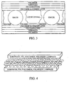
- the light source is then turned on only on one side, resulting in a deposition of any of the remaining polymer along the substrate closest to the light source as shown in figure 3.
- This particular embodiment can be further refined by using liquid crystals capable of bistability, i.e., the ability to maintain two or more electrooptic states without any electric field being present.
- bistable or multistable liquid crystal are those of the ferroelectric or anti-ferroelectric type.
- the reaction rate is varied during the course of polymerization to create a structure in which liquid crystal droplets interspersed in the polymer are created on the alignment surface nearest to the light source and a thin layer of the liquid crystal is created on the alignment surface opposite the light source as shown in figure 4. Both surfaces are aligned in such a configuration so as to produce alignment of the LC molecules on both surfaces, but droplet-encapsulated LC is known to be a more durable structure in terms of maintaining bistability.
- a liquid crystal display device is assembled using the following procedure:
- non-structural PIE elements are larger than 50% of the spacer size, they will be distributed on a roughly two-dimensional, random lattice network. Upon polymerization, the polymer will grow from the PIE's in an approximately spherical shape, which with sufficient polymerization will extend onto the substrates, providing localized polymer attachment between the substrates.
- NSPIE non-structural PIE
- an open-celled, integral network of polymer spheroids is formed with the LC filling the inter-polymer regions ( Figure 6).
- This particular structure is useful for bistable displays in that it provides a high density of mechanical discontinuities that increase optical hysteresis necessary for bistability, as well as added durability.
- the polymerization initiator is not activated by light but rather is the accelerator lacquer' type.
- coating of the spacers or NSPIE elements is accomplished via the method as previously described, but the polymerization begins to occur automatically at some time after the LC/polymer mixture is brought into contact with the initiator-coated spacers or NSPIE elements. Lamination is performed at room temperature in order to lengthen the time before cure begins. After lamination has been completed, the temperature is raised in order to increase the diffusivity of the LC and pre-polymer.
- aromatic amines in the pre-polymer formulation and the peroxide in the lacquer are chosen so as to provide the correct free radical generation rate which, when combined with the diffusion rates of the pre-polymer and LC and the spacings within the display region, result in the polymer localized to the region surrounding the spacers or NSPIE elements.
- the NSPIE elements may be glass or plastic spheres or rods typically used in display devices, but in this case smaller than the spacer elements for this particular display. Because the NSPIE elements are only in contact with, at most, one substrate, the NSPIE elements are not pressed against the substrates with excessive force during compression. As a result, the NSPIE elements may be of non-smooth shapes without causing damage to the substrates during compression. In addition, because the NSPIE elements aren't used to determine substrate spacing, they can be of widely varying shapes and sizes and still perform their function satisfactorily. These factors allow for the use of a much wider variety of materials for NSPIE elements than would be possible for standard spacer elements.
- nanporous materials For instance, a new class or materials, termed nanporous materials, is becoming available in which the pore size as well as total surface area can be specified and fabricated. These materials are typically ceramic or silica composites, formed by sintering, aerosol methods, or by chemical treatment of pre-existing minerals or glass. In nearly all these cases, however, the resulting particles are of poorly controlled size and/or shape, and often of a rough and sometimes sharp surface - they could not be used as spacer elements within the display device. As NSPIE elements, however, their porosity can be controlled to provide a relatively predetermined volumetric reservoir of photoinitiator, accelerator or other polymerization enhancement component.
- the NSPIE elements may also be deposited directly onto the substrates prior to assembly. This would typically be done in conjunction with NSPIE elements mixed into the LC ⁇ pre-polymer mix and would provide stronger bonding of the polymer to the substrate.
- Two or more photoinitiators with different spectral sensitivities may be used to control when polymerization is initiated at a particular site. Since scission of the photoinitiator occurs when the photon energy of the light source exceeds a certain threshold, photoinitiators will typically be sensitive to light of wavelengths less than a specific value; thus, a photoinitiator sensitive to visible light will usually also be sensitive to ultraviolet light.
- One embodiment using this feature would be to coat the spacer elements with a visible light sensitive photoinitiator and to coat the NSPIE elements with a UV sensitive photoinitiator. The assembly is first exposed to visible light, resulting in the curing of only the polymer around the spacers. The assembly is then exposed to UV light, causing curing of any additional pre-polymer still in solution with the LC.
- NSPIE elements deposited on the substrates may have an additive that improves elongation before tear but decreasing the material's durometer (thus making it more susceptible to compression), while NSPIE elements mixed into the LC/polymer mix may not have such an additive and thus be of a higher durometer. In such a way, peel strength can be further enhanced.
- Acrylic adhesives which have excellent optical clarity as well as the availability of a wide selection of manufactured optical grade versions of the material.
- Other polymers that might also be used are, for instance, epoxies or urethanes, though typically these classes of polymers do not have the optical properties equal to those of the acrylics.
- Acrylic adhesives are reactive cross-linldng structural adhesives that cure by means of free-radical initiation. They are based on the methacrylate monomers and cure by addition polymerization. The formation of free radicals initiates a sudden and rapid chain reaction and curing of the adhesive. Condensation polymerization, on the other hand, typified by urethane and epoxies, proceeds at an approximately constant, usually lower reaction rate.
- Acrylics can also be cured by exposure to ultraviolet light less than 400nm in wavelength, and in some instances by light in the visible range as well.
- the free radical source is termed a photoinitiator and results in the formation of free radicals on exposure to light.
- Compounds which act as photoinitiators with light in the range of 200 - 300 nm are benzoine ethers, activated benzophenones and related compounds; benzyl dialkyl amino morpholinyl ketone is an example of a visible wavelength-activated photoinitiator.
- Photoinitiators are disassociated into segments forming free radicals by light in a process known as scission.
- One example of an equal mix curing system is embodied in U.S.
- Patent No. 4,331,795 which uses a cobalt salt accelerator in one component and a hydroperoxide in the other element.
- Epoxies may also be formulated that can be UV-cured via cationic polymerization by incorporating reactive diluents and cyclic monomers. UV-initiated cationic curing of urethanes may be accomplished, for instance, by basing the formation on vinyl ether and polyurethane oligomers such as that manufactured by Allied Signal Inc.
- the PIE material may supply a constituent component of the pre-polymer that is essential to the initiation of curing but that is left out of the LC/pre-polymer mixture. That essential constituent is part of the PIE material and is deposited at one or more of the desired spacing elements within the display region, thus ensuring that initiation and cure will proceed from the desired locations only.
- the just-mentioned essential constituent component may be a photoinitiator, which is activated when exposed to either UV or visible light via scission.
- the rate of photopolymerization may be controlled by adjusting the intensity of the light source.
- the rate of diffusion of the phase separation process may be controlled by adjusting the temperature at which the reaction occurs.
- the rate of the photopolymerization may be varied during the course of the polymerization process in order to create multilayer, composite polymer/LC structures.
- the rate of the phase separation may be controlled by adjusting the miscibility of the LC and the pre-polymer.
- the rate of the phase separation may be controlled by adjusting the absolute and relative viscosities of the LC and the pre-polymer.
- the spacer elements may be coated with an accelerator lacquer or photoinitiator prior to device assembly and then dry-spray deposited onto one or more of the substrates.
- the spacer elements may be deposited via a wet-spray method in which the solution used as the deposition vehicle is either strictly composed of an accelerator or photoinitiator, or includes either or both of these compounds and a solvent, the concentration of which is adjusted to achieve the appropriate quantity of material to fully polymerize the pre-polymer within the display region around the spacers.
- the spacers may be mixed into a solution of the accelerator or_ photoinitiator.
- the solution is then dispensed in liquid form, via a method such as a pipette, silk screen or syringe, directly onto macroscopic regions on the substrates.
- the macroscopic region might be the outside perimeter, thereby automatically achieving an edge seal of the display during polymerization.
- the spacer elements may be porous structures, and the accelerator or photoinitiator is then allowed to absorb into the porous matrix in order to increase the weight percent of accelerator or photoinitiator in the desired localized region as well as to provide better interpenetration of the polymer and spacer elements, thus providing better adhesion.
- the spacer elements may be composed of glass, typically in the form of beads or rods, which are then etched to increase the surface area for improved adhesion.
- One or more layers of a an adhesion promoter such as a silane coupling agent may be coated onto the glass spacers which may or may not have been etched, prior to the coating of the glass spacers with the accelerator or photoinitiator.
- the spacer elements may be admixed to the photoinitiator or accelerator in concentrations higher than what would be desired in regions of the display that are active image areas; the mixture is then deposited onto the substrate via printing or pipette methods into the interpixel regions or the perimeter where no image is presented, thus providing additional support without adversely affecting the image contrast or quality.
- the initiator may be solely heat activated or heat activated as well as photo-activated or other activation method.
- the polymer is chosen so as to contract following initial bonding to the substrates and upon curing; the two substrates are thus drawn together, increasing durability of the display; this is particularly effective when the polymer is localized around the spacer element, as has been previously described.
- the spacer element may be one or more sheets of an extensible porous membrane that when laminated in between the substrates is the element that determines the spacing between the substrates.
- one or more of substrates may be glass or other rigid material.
- the photoinitiator, accelerator, or other polymerization enhancement material is coated onto or contained within the non-structural PIE (NSPIE) element.
Landscapes
- Physics & Mathematics (AREA)
- Nonlinear Science (AREA)
- Chemical & Material Sciences (AREA)
- Crystallography & Structural Chemistry (AREA)
- General Physics & Mathematics (AREA)
- Optics & Photonics (AREA)
- Mathematical Physics (AREA)
- Dispersion Chemistry (AREA)
- Liquid Crystal (AREA)
- Polymerisation Methods In General (AREA)
Applications Claiming Priority (5)
| Application Number | Priority Date | Filing Date | Title |
|---|---|---|---|
| US26823501P | 2001-02-12 | 2001-02-12 | |
| US268235P | 2001-02-12 | ||
| US09/883,083 US6618114B2 (en) | 2001-02-12 | 2001-06-15 | Electrooptical displays with multilayer structure achieved by varying rates of polymerization and/or phase separation during the course of polymerization |
| US883083 | 2001-06-15 | ||
| PCT/US2002/004067 WO2002073299A1 (en) | 2001-02-12 | 2002-02-12 | Electrooptical displays with multilayer structure achieved by varying rates of polymerization and/or phase separation |
Publications (3)
| Publication Number | Publication Date |
|---|---|
| EP1360548A1 EP1360548A1 (en) | 2003-11-12 |
| EP1360548A4 EP1360548A4 (en) | 2005-07-20 |
| EP1360548B1 true EP1360548B1 (en) | 2006-11-29 |
Family
ID=26952961
Family Applications (1)
| Application Number | Title | Priority Date | Filing Date |
|---|---|---|---|
| EP02723135A Expired - Lifetime EP1360548B1 (en) | 2001-02-12 | 2002-02-12 | Electrooptical displays with multilayer structure achieved by varying rates of polymerization |
Country Status (6)
| Country | Link |
|---|---|
| EP (1) | EP1360548B1 (cg-RX-API-DMAC10.html) |
| JP (1) | JP4034186B2 (cg-RX-API-DMAC10.html) |
| KR (1) | KR100831236B1 (cg-RX-API-DMAC10.html) |
| CN (1) | CN1276294C (cg-RX-API-DMAC10.html) |
| AT (1) | ATE347123T1 (cg-RX-API-DMAC10.html) |
| DE (1) | DE60216420T2 (cg-RX-API-DMAC10.html) |
Families Citing this family (4)
| Publication number | Priority date | Publication date | Assignee | Title |
|---|---|---|---|---|
| US20080084522A1 (en) * | 2006-10-06 | 2008-04-10 | Chung Yuan Christian University | Liquid Crystal Device with Stratified Phase-separated Composite and Method for Forming the Same |
| DE102006052606B4 (de) | 2006-11-08 | 2008-09-18 | Leonhard Kurz Gmbh & Co. Kg | Verfahren zur Herstellung von PDLCDs |
| KR101010579B1 (ko) * | 2008-12-17 | 2011-01-24 | (주)에이엔티이십일 | 다단 산기장치 |
| DE102010010448A1 (de) | 2010-03-01 | 2011-09-01 | LÜTH & DÜMCHEN Automatisierungsprojekt GmbH | Materialien, die in ihrer optischen Ansicht auf elektrischem oder elektronischem Wege veränderbar sind, und Verfahren und Einrichtung zum Aufbringen von Grafiken auf diese Materialien |
Citations (1)
| Publication number | Priority date | Publication date | Assignee | Title |
|---|---|---|---|---|
| EP0987581A2 (en) * | 1993-12-27 | 2000-03-22 | Matsushita Electric Industrial Co., Ltd. | Liquid-crystal panel, method of manufacturing the same, and liquid-crystal display apparatus |
Family Cites Families (4)
| Publication number | Priority date | Publication date | Assignee | Title |
|---|---|---|---|---|
| JP2831521B2 (ja) * | 1992-12-17 | 1998-12-02 | シャープ株式会社 | 強誘電性液晶表示素子及びその製造方法 |
| KR100277626B1 (ko) * | 1993-06-23 | 2001-01-15 | 김순택 | 액정 표시장치의 제조방법 |
| JP3068400B2 (ja) * | 1994-03-17 | 2000-07-24 | シャープ株式会社 | 液晶表示装置の製造方法 |
| JP2000206515A (ja) * | 1998-11-13 | 2000-07-28 | Matsushita Electric Ind Co Ltd | 調光体、光学的素子及び電気的素子、並びにその製造方法 |
-
2002
- 2002-02-12 AT AT02723135T patent/ATE347123T1/de not_active IP Right Cessation
- 2002-02-12 DE DE60216420T patent/DE60216420T2/de not_active Expired - Lifetime
- 2002-02-12 EP EP02723135A patent/EP1360548B1/en not_active Expired - Lifetime
- 2002-02-12 KR KR1020027009595A patent/KR100831236B1/ko not_active Expired - Lifetime
- 2002-02-12 CN CNB028070291A patent/CN1276294C/zh not_active Expired - Lifetime
- 2002-02-12 JP JP2002572494A patent/JP4034186B2/ja not_active Expired - Lifetime
Patent Citations (1)
| Publication number | Priority date | Publication date | Assignee | Title |
|---|---|---|---|---|
| EP0987581A2 (en) * | 1993-12-27 | 2000-03-22 | Matsushita Electric Industrial Co., Ltd. | Liquid-crystal panel, method of manufacturing the same, and liquid-crystal display apparatus |
Also Published As
| Publication number | Publication date |
|---|---|
| DE60216420D1 (de) | 2007-01-11 |
| CN1276294C (zh) | 2006-09-20 |
| DE60216420T2 (de) | 2007-10-04 |
| JP2004523802A (ja) | 2004-08-05 |
| KR20030068391A (ko) | 2003-08-21 |
| EP1360548A4 (en) | 2005-07-20 |
| KR100831236B1 (ko) | 2008-05-22 |
| EP1360548A1 (en) | 2003-11-12 |
| ATE347123T1 (de) | 2006-12-15 |
| CN1503922A (zh) | 2004-06-09 |
| JP4034186B2 (ja) | 2008-01-16 |
Similar Documents
| Publication | Publication Date | Title |
|---|---|---|
| US6812991B2 (en) | Electrooptical displays with polymer localized in vicinities of substrate spacers | |
| US6621548B2 (en) | Electrooptical displays constructed with polymer-coated elements positioned between substrates | |
| US6697143B2 (en) | Electrooptical displays constructed with polymerization initiating and enhancing elements positioned between substrates | |
| US6618114B2 (en) | Electrooptical displays with multilayer structure achieved by varying rates of polymerization and/or phase separation during the course of polymerization | |
| US20050270468A1 (en) | Liquid crystal display device and manufacturing method thereof | |
| EP1377873B1 (en) | Liquid crystal displays constructed with polymerization initiating and enhancing elements positioned between substrates | |
| EP1360548A1 (en) | Electrooptical displays with multilayer structure achieved by varying rates of polymerization and/or phase separation | |
| JP2005506558A5 (cg-RX-API-DMAC10.html) | ||
| JP2004523802A5 (cg-RX-API-DMAC10.html) | ||
| JP3059030B2 (ja) | 液晶表示素子及びその製造方法 | |
| JP5180579B2 (ja) | 液晶光学装置 | |
| TW583476B (en) | Display device and fabrication method thereof |
Legal Events
| Date | Code | Title | Description |
|---|---|---|---|
| PUAI | Public reference made under article 153(3) epc to a published international application that has entered the european phase |
Free format text: ORIGINAL CODE: 0009012 |
|
| 17P | Request for examination filed |
Effective date: 20030812 |
|
| AK | Designated contracting states |
Kind code of ref document: A1 Designated state(s): AT BE CH CY DE DK ES FI FR GB GR IE IT LI LU MC NL PT SE TR |
|
| AX | Request for extension of the european patent |
Extension state: AL LT LV MK RO SI |
|
| REG | Reference to a national code |
Ref country code: DE Ref legal event code: R079 Ref document number: 60216420 Country of ref document: DE Free format text: PREVIOUS MAIN CLASS: G02F0001133300 Ipc: G02F0001133400 |
|
| A4 | Supplementary search report drawn up and despatched |
Effective date: 20050603 |
|
| RIC1 | Information provided on ipc code assigned before grant |
Ipc: 7G 02F 1/1339 B Ipc: 7G 02F 1/1334 A |
|
| GRAP | Despatch of communication of intention to grant a patent |
Free format text: ORIGINAL CODE: EPIDOSNIGR1 |
|
| RTI1 | Title (correction) |
Free format text: ELECTROOPTICAL DISPLAYS WITH MULTILAYER STRUCTURE ACHIEVED BY VARYING RATES OF POLYMERIZATION |
|
| RAP1 | Party data changed (applicant data changed or rights of an application transferred) |
Owner name: SAMSUNG ELECTRONICS CO., LTD. |
|
| GRAS | Grant fee paid |
Free format text: ORIGINAL CODE: EPIDOSNIGR3 |
|
| GRAA | (expected) grant |
Free format text: ORIGINAL CODE: 0009210 |
|
| AK | Designated contracting states |
Kind code of ref document: B1 Designated state(s): AT BE CH CY DE DK ES FI FR GB GR IE IT LI LU MC NL PT SE TR |
|
| PG25 | Lapsed in a contracting state [announced via postgrant information from national office to epo] |
Ref country code: IT Free format text: LAPSE BECAUSE OF FAILURE TO SUBMIT A TRANSLATION OF THE DESCRIPTION OR TO PAY THE FEE WITHIN THE PRESCRIBED TIME-LIMIT;WARNING: LAPSES OF ITALIAN PATENTS WITH EFFECTIVE DATE BEFORE 2007 MAY HAVE OCCURRED AT ANY TIME BEFORE 2007. THE CORRECT EFFECTIVE DATE MAY BE DIFFERENT FROM THE ONE RECORDED. Effective date: 20061129 Ref country code: FI Free format text: LAPSE BECAUSE OF FAILURE TO SUBMIT A TRANSLATION OF THE DESCRIPTION OR TO PAY THE FEE WITHIN THE PRESCRIBED TIME-LIMIT Effective date: 20061129 Ref country code: NL Free format text: LAPSE BECAUSE OF FAILURE TO SUBMIT A TRANSLATION OF THE DESCRIPTION OR TO PAY THE FEE WITHIN THE PRESCRIBED TIME-LIMIT Effective date: 20061129 Ref country code: CH Free format text: LAPSE BECAUSE OF FAILURE TO SUBMIT A TRANSLATION OF THE DESCRIPTION OR TO PAY THE FEE WITHIN THE PRESCRIBED TIME-LIMIT Effective date: 20061129 Ref country code: LI Free format text: LAPSE BECAUSE OF FAILURE TO SUBMIT A TRANSLATION OF THE DESCRIPTION OR TO PAY THE FEE WITHIN THE PRESCRIBED TIME-LIMIT Effective date: 20061129 Ref country code: AT Free format text: LAPSE BECAUSE OF FAILURE TO SUBMIT A TRANSLATION OF THE DESCRIPTION OR TO PAY THE FEE WITHIN THE PRESCRIBED TIME-LIMIT Effective date: 20061129 Ref country code: BE Free format text: LAPSE BECAUSE OF FAILURE TO SUBMIT A TRANSLATION OF THE DESCRIPTION OR TO PAY THE FEE WITHIN THE PRESCRIBED TIME-LIMIT Effective date: 20061129 |
|
| REG | Reference to a national code |
Ref country code: GB Ref legal event code: FG4D |
|
| REG | Reference to a national code |
Ref country code: CH Ref legal event code: EP |
|
| REG | Reference to a national code |
Ref country code: IE Ref legal event code: FG4D |
|
| REF | Corresponds to: |
Ref document number: 60216420 Country of ref document: DE Date of ref document: 20070111 Kind code of ref document: P |
|
| REG | Reference to a national code |
Ref country code: DE Ref legal event code: R096 Ref document number: 60216420 Country of ref document: DE Effective date: 20070111 |
|
| PG25 | Lapsed in a contracting state [announced via postgrant information from national office to epo] |
Ref country code: MC Free format text: LAPSE BECAUSE OF NON-PAYMENT OF DUE FEES Effective date: 20070228 Ref country code: SE Free format text: LAPSE BECAUSE OF FAILURE TO SUBMIT A TRANSLATION OF THE DESCRIPTION OR TO PAY THE FEE WITHIN THE PRESCRIBED TIME-LIMIT Effective date: 20070228 Ref country code: DK Free format text: LAPSE BECAUSE OF FAILURE TO SUBMIT A TRANSLATION OF THE DESCRIPTION OR TO PAY THE FEE WITHIN THE PRESCRIBED TIME-LIMIT Effective date: 20070228 |
|
| PG25 | Lapsed in a contracting state [announced via postgrant information from national office to epo] |
Ref country code: ES Free format text: LAPSE BECAUSE OF FAILURE TO SUBMIT A TRANSLATION OF THE DESCRIPTION OR TO PAY THE FEE WITHIN THE PRESCRIBED TIME-LIMIT Effective date: 20070312 |
|
| PG25 | Lapsed in a contracting state [announced via postgrant information from national office to epo] |
Ref country code: PT Free format text: LAPSE BECAUSE OF FAILURE TO SUBMIT A TRANSLATION OF THE DESCRIPTION OR TO PAY THE FEE WITHIN THE PRESCRIBED TIME-LIMIT Effective date: 20070430 |
|
| NLV1 | Nl: lapsed or annulled due to failure to fulfill the requirements of art. 29p and 29m of the patents act | ||
| REG | Reference to a national code |
Ref country code: CH Ref legal event code: PL |
|
| EN | Fr: translation not filed | ||
| PLBE | No opposition filed within time limit |
Free format text: ORIGINAL CODE: 0009261 |
|
| STAA | Information on the status of an ep patent application or granted ep patent |
Free format text: STATUS: NO OPPOSITION FILED WITHIN TIME LIMIT |
|
| 26N | No opposition filed |
Effective date: 20070830 |
|
| REG | Reference to a national code |
Ref country code: DE Ref legal event code: R097 Ref document number: 60216420 Country of ref document: DE Effective date: 20070830 |
|
| PG25 | Lapsed in a contracting state [announced via postgrant information from national office to epo] |
Ref country code: IE Free format text: LAPSE BECAUSE OF NON-PAYMENT OF DUE FEES Effective date: 20070212 |
|
| PG25 | Lapsed in a contracting state [announced via postgrant information from national office to epo] |
Ref country code: FR Free format text: LAPSE BECAUSE OF FAILURE TO SUBMIT A TRANSLATION OF THE DESCRIPTION OR TO PAY THE FEE WITHIN THE PRESCRIBED TIME-LIMIT Effective date: 20070720 Ref country code: GR Free format text: LAPSE BECAUSE OF FAILURE TO SUBMIT A TRANSLATION OF THE DESCRIPTION OR TO PAY THE FEE WITHIN THE PRESCRIBED TIME-LIMIT Effective date: 20070301 |
|
| PG25 | Lapsed in a contracting state [announced via postgrant information from national office to epo] |
Ref country code: FR Free format text: LAPSE BECAUSE OF FAILURE TO SUBMIT A TRANSLATION OF THE DESCRIPTION OR TO PAY THE FEE WITHIN THE PRESCRIBED TIME-LIMIT Effective date: 20061129 |
|
| PG25 | Lapsed in a contracting state [announced via postgrant information from national office to epo] |
Ref country code: LU Free format text: LAPSE BECAUSE OF NON-PAYMENT OF DUE FEES Effective date: 20070212 Ref country code: CY Free format text: LAPSE BECAUSE OF FAILURE TO SUBMIT A TRANSLATION OF THE DESCRIPTION OR TO PAY THE FEE WITHIN THE PRESCRIBED TIME-LIMIT Effective date: 20061129 |
|
| PG25 | Lapsed in a contracting state [announced via postgrant information from national office to epo] |
Ref country code: TR Free format text: LAPSE BECAUSE OF FAILURE TO SUBMIT A TRANSLATION OF THE DESCRIPTION OR TO PAY THE FEE WITHIN THE PRESCRIBED TIME-LIMIT Effective date: 20061129 |
|
| REG | Reference to a national code |
Ref country code: GB Ref legal event code: 732E Free format text: REGISTERED BETWEEN 20130307 AND 20130313 |
|
| REG | Reference to a national code |
Ref country code: DE Ref legal event code: R082 Ref document number: 60216420 Country of ref document: DE Representative=s name: DR. WEITZEL & PARTNER, DE |
|
| REG | Reference to a national code |
Ref country code: DE Ref legal event code: R081 Ref document number: 60216420 Country of ref document: DE Owner name: SAMSUNG DISPLAY CO., LTD., KR Free format text: FORMER OWNER: SAMSUNG ELECTRONICS CO., LTD., SUWON-SI, KR Effective date: 20130422 Ref country code: DE Ref legal event code: R082 Ref document number: 60216420 Country of ref document: DE Representative=s name: DR. WEITZEL & PARTNER, DE Effective date: 20130422 Ref country code: DE Ref legal event code: R082 Ref document number: 60216420 Country of ref document: DE Representative=s name: SCHIEBER - FARAGO, DE Effective date: 20130422 Ref country code: DE Ref legal event code: R081 Ref document number: 60216420 Country of ref document: DE Owner name: SAMSUNG DISPLAY CO., LTD., YONGIN-CITY, KR Free format text: FORMER OWNER: SAMSUNG ELECTRONICS CO., LTD., SUWON-SI, GYEONGGI-DO, KR Effective date: 20130422 Ref country code: DE Ref legal event code: R081 Ref document number: 60216420 Country of ref document: DE Owner name: HYDIS TECHNOLOGIES CO., LTD., KR Free format text: FORMER OWNER: SAMSUNG ELECTRONICS CO., LTD., SUWON-SI, GYEONGGI-DO, KR Effective date: 20130422 Ref country code: DE Ref legal event code: R081 Ref document number: 60216420 Country of ref document: DE Owner name: HYDIS TECHNOLOGIES CO., LTD., KR Free format text: FORMER OWNER: VIZTEC INC., TAMPA, FLA., US Effective date: 20061102 Ref country code: DE Ref legal event code: R082 Ref document number: 60216420 Country of ref document: DE Representative=s name: FARAGO PATENTANWALTS- UND RECHTSANWALTSGESELLS, DE Effective date: 20130422 Ref country code: DE Ref legal event code: R082 Ref document number: 60216420 Country of ref document: DE Representative=s name: FARAGO PATENTANWAELTE, DE Effective date: 20130422 |
|
| REG | Reference to a national code |
Ref country code: DE Ref legal event code: R082 Ref document number: 60216420 Country of ref document: DE Representative=s name: SCHIEBER - FARAGO, DE Ref country code: DE Ref legal event code: R082 Ref document number: 60216420 Country of ref document: DE Representative=s name: FARAGO PATENTANWALTS- UND RECHTSANWALTSGESELLS, DE Ref country code: DE Ref legal event code: R082 Ref document number: 60216420 Country of ref document: DE Representative=s name: FARAGO PATENTANWAELTE, DE |
|
| REG | Reference to a national code |
Ref country code: GB Ref legal event code: 732E Free format text: REGISTERED BETWEEN 20210107 AND 20210113 |
|
| PGFP | Annual fee paid to national office [announced via postgrant information from national office to epo] |
Ref country code: DE Payment date: 20210304 Year of fee payment: 20 Ref country code: GB Payment date: 20210113 Year of fee payment: 20 |
|
| REG | Reference to a national code |
Ref country code: DE Ref legal event code: R082 Ref document number: 60216420 Country of ref document: DE Representative=s name: FARAGO PATENTANWALTS- UND RECHTSANWALTSGESELLS, DE Ref country code: DE Ref legal event code: R081 Ref document number: 60216420 Country of ref document: DE Owner name: HYDIS TECHNOLOGIES CO., LTD., KR Free format text: FORMER OWNER: SAMSUNG DISPLAY CO., LTD., YONGIN-CITY, GYEONGGI-DO, KR |
|
| REG | Reference to a national code |
Ref country code: DE Ref legal event code: R071 Ref document number: 60216420 Country of ref document: DE |
|
| REG | Reference to a national code |
Ref country code: GB Ref legal event code: PE20 Expiry date: 20220211 |
|
| PG25 | Lapsed in a contracting state [announced via postgrant information from national office to epo] |
Ref country code: GB Free format text: LAPSE BECAUSE OF EXPIRATION OF PROTECTION Effective date: 20220211 |
|
| P01 | Opt-out of the competence of the unified patent court (upc) registered |
Effective date: 20230516 |