EP1353373A2 - Hermetically sealed package for an electronic component - Google Patents
Hermetically sealed package for an electronic component Download PDFInfo
- Publication number
- EP1353373A2 EP1353373A2 EP03100819A EP03100819A EP1353373A2 EP 1353373 A2 EP1353373 A2 EP 1353373A2 EP 03100819 A EP03100819 A EP 03100819A EP 03100819 A EP03100819 A EP 03100819A EP 1353373 A2 EP1353373 A2 EP 1353373A2
- Authority
- EP
- European Patent Office
- Prior art keywords
- base
- lid
- layer
- package
- component
- Prior art date
- Legal status (The legal status is an assumption and is not a legal conclusion. Google has not performed a legal analysis and makes no representation as to the accuracy of the status listed.)
- Granted
Links
Images

Classifications
-
- B—PERFORMING OPERATIONS; TRANSPORTING
- B81—MICROSTRUCTURAL TECHNOLOGY
- B81B—MICROSTRUCTURAL DEVICES OR SYSTEMS, e.g. MICROMECHANICAL DEVICES
- B81B7/00—Microstructural systems ; Auxiliary parts of microstructural devices or systems
- B81B7/0032—Packages or encapsulation
- B81B7/007—Interconnections between the MEMS and external electrical signals
-
- B—PERFORMING OPERATIONS; TRANSPORTING
- B81—MICROSTRUCTURAL TECHNOLOGY
- B81B—MICROSTRUCTURAL DEVICES OR SYSTEMS, e.g. MICROMECHANICAL DEVICES
- B81B7/00—Microstructural systems ; Auxiliary parts of microstructural devices or systems
- B81B7/0006—Interconnects
-
- H—ELECTRICITY
- H10—SEMICONDUCTOR DEVICES; ELECTRIC SOLID-STATE DEVICES NOT OTHERWISE PROVIDED FOR
- H10W—GENERIC PACKAGES, INTERCONNECTIONS, CONNECTORS OR OTHER CONSTRUCTIONAL DETAILS OF DEVICES COVERED BY CLASS H10
- H10W76/00—Containers; Fillings or auxiliary members therefor; Seals
- H10W76/60—Seals
-
- H—ELECTRICITY
- H10—SEMICONDUCTOR DEVICES; ELECTRIC SOLID-STATE DEVICES NOT OTHERWISE PROVIDED FOR
- H10W—GENERIC PACKAGES, INTERCONNECTIONS, CONNECTORS OR OTHER CONSTRUCTIONAL DETAILS OF DEVICES COVERED BY CLASS H10
- H10W95/00—Packaging processes not covered by the other groups of this subclass
-
- H—ELECTRICITY
- H10—SEMICONDUCTOR DEVICES; ELECTRIC SOLID-STATE DEVICES NOT OTHERWISE PROVIDED FOR
- H10W—GENERIC PACKAGES, INTERCONNECTIONS, CONNECTORS OR OTHER CONSTRUCTIONAL DETAILS OF DEVICES COVERED BY CLASS H10
- H10W72/00—Interconnections or connectors in packages
- H10W72/50—Bond wires
- H10W72/551—Materials of bond wires
- H10W72/552—Materials of bond wires comprising metals or metalloids, e.g. silver
-
- H—ELECTRICITY
- H10—SEMICONDUCTOR DEVICES; ELECTRIC SOLID-STATE DEVICES NOT OTHERWISE PROVIDED FOR
- H10W—GENERIC PACKAGES, INTERCONNECTIONS, CONNECTORS OR OTHER CONSTRUCTIONAL DETAILS OF DEVICES COVERED BY CLASS H10
- H10W72/00—Interconnections or connectors in packages
- H10W72/851—Dispositions of multiple connectors or interconnections
- H10W72/874—On different surfaces
- H10W72/884—Die-attach connectors and bond wires
-
- Y—GENERAL TAGGING OF NEW TECHNOLOGICAL DEVELOPMENTS; GENERAL TAGGING OF CROSS-SECTIONAL TECHNOLOGIES SPANNING OVER SEVERAL SECTIONS OF THE IPC; TECHNICAL SUBJECTS COVERED BY FORMER USPC CROSS-REFERENCE ART COLLECTIONS [XRACs] AND DIGESTS
- Y10—TECHNICAL SUBJECTS COVERED BY FORMER USPC
- Y10S—TECHNICAL SUBJECTS COVERED BY FORMER USPC CROSS-REFERENCE ART COLLECTIONS [XRACs] AND DIGESTS
- Y10S438/00—Semiconductor device manufacturing: process
- Y10S438/928—Front and rear surface processing
-
- Y—GENERAL TAGGING OF NEW TECHNOLOGICAL DEVELOPMENTS; GENERAL TAGGING OF CROSS-SECTIONAL TECHNOLOGIES SPANNING OVER SEVERAL SECTIONS OF THE IPC; TECHNICAL SUBJECTS COVERED BY FORMER USPC CROSS-REFERENCE ART COLLECTIONS [XRACs] AND DIGESTS
- Y10—TECHNICAL SUBJECTS COVERED BY FORMER USPC
- Y10S—TECHNICAL SUBJECTS COVERED BY FORMER USPC CROSS-REFERENCE ART COLLECTIONS [XRACs] AND DIGESTS
- Y10S438/00—Semiconductor device manufacturing: process
- Y10S438/977—Thinning or removal of substrate
Definitions
- the present invention relates to the field of electronics and, more particularly, to hermetic packages for electric components.
- Electric components are used in a wide range of applications. In many applications it is necessary to protect the electric components from the environments in which they operate. For example, electric components used in environments with high humidity need to be protected from this humidity to prevent corrosion of their electrical connections. Typically, electric components are protected by sealing them within a ceramic or semiconductor package.
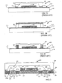
- FIG. 1A depicts a prior art ceramic package 102 for protecting electric components.
- An electric component 100 is packaged by attaching the electric component 100 to a base 104 made of a ceramic material and, then, attaching a lid 106 having a cavity 108 for accommodating the electric component 100 to the base 104 with a sealing material 110.
- Connections for control and input/output (I/O) signals are made to the electric component 100 from outside the package 102 through electrical leads 112 that extend along the surface of the base 104 through the sealing material 110 between the base 104 and the lid 106. Since the electrical leads 112 extend through the sealing material 110, the sealing material 110 must be nonconductive and, therefore, conventional soldering techniques cannot be used to attach the lid 106 to the base 104.
- the lid 106 has a surface area that is smaller than the surface area of the base 104 to provide a suitable planar bonding area 114 on the exterior of the package 102 for facilitating contact with the electrical leads 112. Since the surface area of the lid 106 is smaller than the surface area of the base 104 (and accommodates the electric component 100), the base 104 has a relatively large footprint in relation to the electric component 100. This may be undesirable if a small form factor or a low cost is desired.
- each ceramic package 102 is produced individually using expensive hybrid assembly techniques, rather than inexpensive, mass production, wafer level techniques. Also, ceramic packaging is expensive due to the high cost of raw ceramic material used to create the base 104 and lid 106. Thus, ceramic packaging may be cost prohibitive.
- FIG. 1B depicts an alternative prior art ceramic package 116.
- metallic ink traces 118 are printed on a base 104 made of a ceramic material to provide connections for control and I/O signals. Ceramic side walls 120 are then added to the base 104 over the metallic ink traces 118.
- the electric component 100 is packaged by attaching the electric component 100 to the base 104 and, then, soldering a lid 106 made of a metallic material (or a ceramic material with a metalized seal ring) to the side walls 120.
- the metallic ink traces 118 have an inherent high resistivity that may make the ceramic package 116 unsuitable for certain applications.
- this ceramic package 116 requires a base 104 with a relatively large footprint and uses expensive materials and hybrid assembly techniques.
- FIG. 1C depicts a prior art semiconductor package 122 having a base 104 made of semiconductor material and a lid 106 made of semiconductor material.
- the lid 106 is attached to the base 104 using frit glass 124 (i.e., a powdered glass held together in a slurry).
- the electric component 100 is packaged by attaching the electric component 100 to the base 104, depositing a layer of frit glass 124 on the base 104, attaching the lid 106 to the frit glass 124, and curing the frit glass 124 to produce a sealed semiconductor package 122. Connections for control and I/O signals are made to the electric component 100 from outside the package 102 through electrical leads 112 that extend along the surface of the base 104.
- the semiconductor packaging technique requires a base 104 with a relatively large footprint.
- the temperatures required to cure the frit glass 124 may be damaging to certain electric components.
- the semiconductor package 122 may be mass produced using wafer packaging techniques. After the package 122 is produced, however, the lid 106 has to be etched precisely to expose a planar bonding area 114 without damaging the electrical leads. This additional step adds complexity, thus increasing production costs.
- the present invention provides an electric component package having a base and a lid that define a sealed cavity therebetween and a method for producing same.
- the inventive electric component package overcomes the aforementioned limitations by incorporating conductive vias that extend through a dielectric base.
- the conductive vias allow control and/or I/O signals associated with an electric component within the sealed cavity to enter the cavity through the base rather than the junction between the base and the lid.
- the electric component package provides preferably a hermetically sealed environment for the electric component that is small, inexpensive, and can be mass produced at the wafer level using conventional equipment.
- One aspect of the present invention consists in an electric component package including a base having a first surface and a second surface opposite the first surface, the base comprising a dielectric material having at least one conductive via extending through the dielectric material between the first and second surfaces; a component located adjacent the first surface of the base, the component having at least one port coupled to the at least one conductive via; and a lid coupled to the first surface of the base, the lid and the base defining a sealed cavity therebetween, the sealed cavity sized to accommodate the component.
- Another aspect of the present invention consists in a method for sealing a component within a package.
- the method includes (a) forming a base having a first surface and a second surface opposite the first surface, the base comprising a dielectric material having at least one conductive via extending between the first and second surfaces; (b) establishing a component on the first surface of the base, the component having at least one port, the at least one port being coupled to the at least one conductive via; (c) forming a lid; and (d) coupling the lid to the first surface of the base, the lid and the base defining a cavity therebetween for accommodating the component.
- Yet another aspect of the present invention consists in a process for fabricating an electric component package having a sealed cavity for accommodating an electric component.
- the process includes etching a semiconductor base layer having first and second opposing surfaces to form at least one pedestal on the first surface, applying a layer of dielectric material to the first surface of the etched semiconductor base layer, grinding the dielectric layer to expose a surface of the at least one pedestal, establishing an electric component on the ground dielectric layer, the electric component having at least one port coupled to the exposed surface of the at least one pedestal, attaching a lid to the ground dielectric layer, the lid having a cavity for accommodating the electric component, and grinding the semiconductor base layer on the second surface to expose the dielectric layer, the at least one pedestal forming a conductive via extending through the dielectric layer.
- Yet another aspect of the present invention consists in a process for fabricating an electric component package having a sealed cavity for accommodating an electric component.
- the process includes forming a substantially dielectric base having at least one conductive via, establishing the electric component on the base, the electric component having at least one port electrically coupled to the at least one via, forming a lid, and attaching the lid to the base, the lid and the base defining a sealed cavity therebetween for accommodating the electric component.
- Figure 1A is a cross-sectional side view of a prior art ceramic electric component package
- Figure 1B is a cross-sectional side view of an alternative prior art ceramic electric component package
- Figure 1C is a cross-sectional side view of a prior art semiconductor component package
- Figure 2 is a cross-sectional side view of an electric component package in accordance with the present invention.
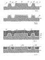
- Figures 3A-H are cross-sectional side views depicting the formation of a base, the establishment of an electric component on the base, and the attachment of a lid to the base to create the electric component package of Figure 2.
- FIG. 2 depicts a cross-sectional side view of a package 200 in accordance with the present invention for housing an electric component 202 within a sealed cavity 204.
- the package 200 includes a base 206 and a lid 208, which define the sealed cavity 204 therebetween.
- the base 206 has at least one via 210 extending therethrough, allowing signals associated with the electric component 202 to pass between the sealed cavity 204 and the exterior of the package 200 without passing through the junction between the base 206 and the lid 208.
- the package 200 is mass produced using wafer level processing techniques and then singulated (i.e., separated from adjacent packages) using conventional dicing techniques.
- the present invention is particularly useful, although not exclusively so, for hermetically sealing environmentally sensitive high frequency electric components, such as semiconductor lasers, and micro electromechanical systems (MEMS).
- MEMS micro electromechanical systems
- the base 206 provides a mounting surface on which the electric component 202 can be mounted and vias 210 extending through the base 206 for passing signals associated with the component 202 such as control, I/O, and/or power signals.
- the via 210 may be used for heat transfer.
- the vias 210 extend between a top surface 206a of the base 206 and a bottom surface 206b of the base 206, and are electrically isolated from one another by a dielectric material 212 having a coefficient of thermal expansion that is approximately equal to that of the vias 210.
- the vias 210 are a conventional semiconductor material such as silicon and the dielectric material 212 is glass (e.g., borosilicate glass).
- the semiconductor material of the vias 210 may be heavily doped and/or the vias 210 may further include a metal sheath 214 (e.g., silver) surrounding the semiconductor material.
- a metal sheath 214 e.g., silver
- Vias 210 surrounded by a metal sheath 214 are especially conductive at high frequencies such as radio frequencies (rf) or microwave frequencies.
- the vias 210 may be comprised entirely of metal.
- the base 206 further includes a seal ring 216 for use in attaching the lid 208 to the base 206, cavity bonding pads 217a for use in establishing the electric component 202 on the base 206 and electrically connecting the component 202 to the vias 210, and external bonding pads 217b for facilitating electrical continuity through the vias 210.
- the seal ring 216 is preferably one or more layers of metal that form a pattern on the base 206 that surrounds the footprint of the electric component 202 and the vias 210 to which the component 202 is coupled.
- the one or more layers of metal that form the seal ring 216 may include a layer of Nichrome and a layer of platinum.
- the bonding pads 217a, b are preferably one or more layers of metal deposited on the exposed surfaces of the via 210.
- the one or more layers of metal that form the cavity bonding pads 217a may include sequential layers of titanium/platinum/gold or titanium/platinum/copper.
- the one or more layers of metal that form the external bonding pads 217b may include sequential layers of titanium/tungsten, copper, and solder (e.g., tin/lead solder).
- solder e.g., tin/lead solder
- the lid 208 is attached to the base 206 to create the sealed cavity 204, which, preferably, is hermetically sealed.
- the lid 208 has a coefficient of thermal expansion that is approximately equal to that of the base 206 and, preferably, is silicon.
- the lid 208 includes a cavity 209 that is sized to accommodate the component 202.
- the lid 208 includes a seal ring 218, which is a mirror image of the base seal ring 216.
- the lid seal ring 218 includes one or more layers of metal, which may include a layer of Nichrome, a layer of platinum, and a layer of solder, such as gold/tin (Au/Sn) solder, for use in bonding the lid seal ring 218 to the base seal ring 216.
- metal such as Nichrome, a layer of platinum, and a layer of solder, such as gold/tin (Au/Sn) solder, for use in bonding the lid seal ring 218 to the base seal ring 216.
- the component 202 is one or more electric components to be sealed within the sealed cavity 204 created by attaching the lid 208 to the base 206.
- the component 202 has one or more ports 220, such as power, control, and/or I/O signal ports, that are connected to the vias 210 that extend through the base 206.
- the component 202 may be a discrete component such as a resistor or capacitor, an integrated circuit with leads that can be wire-bound to the cavity bonding pads 217a deposited on the vias 210, an integrated circuit with a ball grid array (BGA) for solder ball attachment to the cavity bonding pads 217a, a MEMS, or essentially any electric component.
- BGA ball grid array
- FIGs. 3A-H are a series of diagrams illustrating a preferred method for producing the electric component package 200 illustrated in FIG. 2 with like elements having like numbers.
- the method includes (a) forming a base 206 having a first surface 206a and a second surface 206b opposite the first surface 206a, the base 206 including at least one conductive via 210 extending between the first and second surfaces 206a, b (FIGs. 3A-F); (b) attaching a component 202 having at least one port to the first surface 206a of the base 206, the port coupled to a via 210 (FIG.
- the steps are performed at the wafer level using conventional silicon wafer integrated circuit manufacturing machinery and techniques.
- a planar conductive material e.g., silicon
- an etched conductive layer 300 including pedestals 302 and valleys 304.
- the pedestals 302 will form the vias 210 that extend through the base 206 depicted in FIG. 2.
- the valleys 304 are at least 6 mils deep (i.e., the pedestals 302 are at least 6 mils high).
- the etched conductive layer 300 is produced by forming a mask 308 on a planar conductive material.
- the valleys 304 are formed in areas of the planar conductive material that are not shielded by the mask 308; and define the pedestals 302, which are in areas shielded by the mask 308.
- the mask 308 is a silicon nitride material produced on the planar conductive material in a known manner and the planar conductive material is etched using a known KOH and water solution.
- the conductive material may be etched using a known dry etch process. Other suitable etching techniques will be readily apparent to those skilled in the art.
- the mask 308 may be removed in one of several well known manners.
- a metal layer 306 is optionally deposited on the etched surface of the etched conductive layer 300. As will be described below, the metal layer 306 will form the metal sheath 214 surrounding the vias 210 depicted in FIG. 2.
- the metal layer 306 is deposited on the etched surface using conventional techniques. For example, silver may be deposited on the etched surface by evaporating or sputtering a titanium/tungsten layer followed by a silver layer using known techniques. The titanium/tungsten layer acts as an adhesion layer to aid in adhering the silver layer to the surface of the etched conductive layer 300.
- a dielectric material 310 is deposited on the etched conductive layer 300 to fill in the valleys 304.
- the dielectric material 310 is glass, which is applied to the underlying layer (i.e., the etched conductive layer or, if present, the metal layer 304). The glass is fused to the underlying layer through an encapsulation process such as described in commonly assigned United States Patent Nos. 5,268,310 and 5,343,070 to Goodrich et al., incorporated fully herein by reference.
- the dielectric material 310 is ground to expose the top surfaces 302a of the pedestals 302.
- the dielectric material 310 is ground and polished using known techniques to produce a planar specular surface having islands of exposed pedestals 302 separated by dielectric material 310.
- structures 312 are formed on the ground surface of the dielectric material 310 and the top surfaces 302a of the exposed pedestals 302.
- the structures 312 include a seal ring 216 deposited on the dielectric material 310 and cavity bonding pads 217a deposited on the top surface 302a of the exposed pedestals 302.
- the structures 312 may include, by way of example, but is not limited to, fabricated monolithic and heterolithic components (e.g., P-I-N diodes, Schottky diodes, varactor diodes, and resistors) and metal connections between the top surfaces 302a of the exposed pedestals 302. Methods for fabricating heterolithic integrated circuits can be found in commonly assigned United States Patent No. 6,150,197 to Boles et al., incorporated fully herein by reference.
- the seal ring 216 is formed on the ground dielectric material 310 using a conventional dome evaporator to deposit sequentially a layer of Nichrome and a layer of platinum.
- the cavity bonding pads 217a are formed on the top surfaces 302a of the exposed pedestals 302 by depositing sequentially titanium/platinum/gold or titanium/platinum/copper metal layers for use in bonding the component 202 and its associated ports 220 to the base 206.
- the etched conductor layer is ground on a second surface 206b opposite the first surface 206a to expose the dielectric material 310, thereby electrically isolating the pedestals 302 from one another to form the vias 210.
- the external bonding pads 217b are attached to the individual vias 210.
- the final thickness of the base 206 after grinding is approximately 5 mils.
- the external bonding pads 217b are conventional solder bumps created in a known manner by depositing sequentially an adhesion layer (e.g., a layer of titanium/tungsten and a layer of copper) and a solder bump.
- the component 202 is established on the base 206 after the dielectric material 310 is ground and structure 312 is formed on the ground surface (as shown in FIGs. 3D-E) and prior to the etched conductive layer 300 being ground and polished (as shown in FIG. 3F).
- the component 202 may be established on the base 206 immediately following or substantially simultaneously with the step of forming the structure 312 on the base 206 (FIG. 3E).
- Components 202 may be established on the base 206 by bonding discrete components or integrated circuits to the base 206, depositing various metal layers to form components on the base, and/or epitaxially growing components on the base 206.
- the component 202 is established on the base by bonding the component 202 to the base 206 and wire bonding the ports 220 associated with the component 202 to the vias 210.
- Other methods for establishing components 202 on the base 206 will be readily apparent to those skilled in the art.
- the lid 208 is coupled to the base 206 after the component 202 is established on the base 206 (as shown in FIG. 3G) and prior to the etched conductive layer 300 being ground and polished (as shown in FIG. 3F).
- the lid 208 includes preferably a cavity 209 for accommodating the component 202 and a seal ring 218 for attaching the lid 208 to the base 206.
- the lid 208 is created by depositing the lid seal ring 218 on a wafer (e.g., a silicon wafer) and etching the wafer to form the cavity 209.
- the lid seal ring 218 forms a mask on the wafer for use in etching the wafer to create the cavity 209.
- the wafer is then etched using conventional techniques to form the cavity 209.
- the lid seal ring 218 may be formed by depositing photo resist in a desired pattern on the wafer with cutouts for the desired pattern.
- the desired pattern of the lid seal ring 218 is a mirror image of the pattern used to create the base seal ring 216.
- a dome evaporator may be used to deposit sequential layers of metal, such as a layer of Nichrome, a layer of platinum over the Nichrome layer, and then a 5um layer of gold/tin (Au/Sn) solder having a melting point of approximately 300 degrees Celsius.
- solder is used in the preferred embodiment, essentially any solder composition may be used, e.g., Pb/Sn, Sn/Sb, Sn/Cu/G, Au/Ge, Au/Si, etc.
- the photo resist is then dissolved to remove excess metal, leaving the lid seal ring 218.
- the lid 208 is then attached to the base 206.
- the lid 208 is attached to the base 206 by positioning the lid 208 relative to the base 206 using known techniques such that the base seal ring 216 and the lid seal ring 218 are aligned and in contact with one another.
- the seal rings 216, 218 are then heated to a temperature sufficient to reflow the solder on the lid seal ring 218 and, then, cooled to join the lid 208 to the base 206, thereby creating the sealed cavity 204 therebetween.
- the solder used to attached the lid 208 to the base 206 should have a higher reflow temperature than the solder used in the external bonding pads 217b on the base 206 (described in reference to FIG. 3F) to prevent the temperatures used to reflow the solder in the external bonding pads 217b from affecting the junction between the base 206 and the lid 208.
- the electric component package 200 is assembled at wafer level.
- Wafer level assembly is achieved by aligning and joining the wafer on which the bases 206 are fabricated with the wafer on which the lids 208 are fabricated using commercially available wafer aligner/bonders, which are presently used to make Silicon-on-Insulator (SOI) wafers and micro electromechanical (MEM) gas turbines, for example.
- SOI Silicon-on-Insulator
- MEM micro electromechanical
- the base 206 and lid 208 are clamped together within the bonding chamber and the temperature is increased to reflow the solder on the lid ring seal 218.
- the temperature required to reflow the solder is below about 350°C.
- the joined base 206 and lid 208 are then cooled to form the electric component package 200.
- the electric component package 200 is then transferred to an output cassette for singulation using known dicing techniques to separate the package 200 from adjacent devices.
- the type of gas and the pressure of the gas in the bonding chamber can be controlled in a known manner, thus allowing the type of gas and the pressure within the sealed cavity 208 of the electric component package 200 to be controlled.
- the sealed cavity has been described as being defined by a lid having a cavity attached to a base
- the base may be etched (rather than the lid) to form a cavity to define the sealed cavity when attached to the lid, or both the base and the lid may each contain a cavity that, together, define the sealed cavity without departing from the scope of the invention.
Landscapes
- Engineering & Computer Science (AREA)
- Microelectronics & Electronic Packaging (AREA)
- Computer Hardware Design (AREA)
- Micromachines (AREA)
- Piezo-Electric Or Mechanical Vibrators, Or Delay Or Filter Circuits (AREA)
Abstract
Description
Claims (41)
- An electric component package comprising:a base (206) having a first surface (206a) and a second surface (206b) opposite said first surface, said base comprising a dielectric material (212) having at least one conductive via (210) extending through said dielectric material between said first and second surfaces;a component (202) located adjacent said first surface (206a) of said base (206), said component having at least one port (220) coupled to said at least one conductive via (210); anda lid (208) coupled to said first surface (206a) of said base (206), said lid and said base defining a sealed cavity (204) therebetween, said sealed cavity sized to accommodate said component (202).
- A package as claimed in claim 1, wherein said dielectric material (212) is glass and said conductive via (210) comprises silicon.
- A package as claimed in claim 1 or 2, wherein said conductive via (210) comprises a metal sheath (214) surrounding a semiconductor core.
- A package as claimed in claim 3, wherein said metal sheath (214) is silver.
- A package as claimed in any one of the preceding claims, wherein said component (202) is a micro electromechanical structure (MEMS).
- A package as claimed in any one of the preceding claims, wherein said component (202) is a discrete component.
- A package as claimed in any one of the preceding claims 1-5, wherein said component (202) is an integrated circuit (202).
- A package as claimed in claim 7, wherein said at least one port (220) of said integrated circuit (202) is wire bonded to said at least one conductive via (210).
- A package as claimed in claim 7 or 8, wherein said at least one port (220) of said integrated circuit (202) is a solder ball.
- A package as claimed in any one of the preceding claims, wherein said lid (208) is coupled to said first side (206a) of said base (206) with a conductive material (218,216).
- A package as clamed in any one of the preceding claims, wherein said lid (208) is coupled to said first side (206a) of said base with solder.
- A package as claimed in claim 11, wherein said solder has a melting point of less than about 350°C.
- A package as claimed in any one of the preceding claims, including:at least one solder bump (217b) coupled on said second surface (206b) of said base (206) to said at least one conductive via (210).
- A package as claimed in any one of the preceding claims, wherein said base (206) and said lid (208) have approximately equal coefficients of thermal expansion.
- A package as claimed in any one of the preceding claims, wherein said component (202) is hermetically sealed within said sealed cavity (204).
- A method for sealing a component within a package, said method comprising the steps of:(a) forming a base (206) having a first surface (206a) and a second surface (206b) opposite said first surface, said base comprising a dielectric material (212) having at least one conductive via (210) extending between said first and second surfaces;(b) establishing a component (202) on said first surface (206a) of said base (206), said component having at least one port (220), said at least one port being coupled to said at least one conductive via (210);(c) forming a lid (208); and(d) coupling said lid (208) to said first surface (206a) of said base (206), said lid and said base defining a cavity (204) therebetween for accommodating said component (202).
- A method as claimed in claim 16, wherein steps (b) and (d) are performed during step (a).
- A method as claimed in claim 16 or 17, wherein all steps are performed at wafer level.
- A method as claimed in claim 16, 17 or 18, wherein said base (206) and said lid (208) have approximately equal coefficients of thermal expansion.
- A method as claimed in any one of the preceding claims 16 to 19, wherein said component (202) is hermetically sealed within said cavity (204) between said base (206) and said lid (208) when said lid is coupled to said base.
- A process for fabricating an electric component package having a sealed cavity (204) for accommodating an electric component (202), comprising the steps of:etching a semiconductor base layer (300) having first and second opposing surfaces (206a,206b) to form at least one pedestal (302) on said first surface;applying a layer of dielectric material (310) to said first surface (206a) of said etched semiconductor base layer (300);grinding said dielectric layer (310) to expose a surface (302a) of said at least one pedestal (302);establishing an electric component (202) on said ground dielectric layer (310), said electric component having at least one port (220) coupled to said exposed surface (302a) of said at least one pedestal (302);attaching a lid (208) to said ground dielectric layer (310), said lid having a cavity (204) for accommodating said electric component (202); andgrinding said semiconductor base layer (300) on said second surface (206b) to expose said dielectric layer (310), said at least one pedestal (302) forming a conductive via (210) extending through said dielectric layer (310).
- A process as claimed in claim 21, including:depositing a base seal ring (216) on said ground dielectric layer (310), said base seal ring surrounding a footprint of said electric component (202) and said via (210).
- A process as claimed in claim 21 or 22, including the step of fabricating said lid (208) by etching a semiconductor lid layer.
- A process as claimed in claim 23, wherein said lid fabrication step comprises at least the steps of:depositing a lid seal ring (218) on a first surface of said semiconductor lid layer, said lid seal ring coupled to said base seal ring (216) in said attaching step; andetching said first surface of said semiconductor lid layer to form said cavity (204) using said lid seal ring (218) as an etch mask.
- A process as claimed in any one of the preceding claims 21 to 24, including the step of forming a solder bump (217b) on said second surface (206a), said solder bump coupled to said at least one electrically isolated pedestal (210).
- A process as claimed in any one of the preceding claims 21 to 25, said establishing step comprising at least the step of building said component (202) on said ground dielectric layer (206).
- A process as claimed in any one of the preceding claims 21 to 25, said establishing step comprising at least the step of:placing said component (202) on said ground dielectric layer (310).
- A process as claimed in claim 27, wherein said placing step comprises:attaching said component (202) to said ground dielectric layer (310); andelectrically coupling said at least one port (220) to said exposed surface (302a) of said at least one pedestal.
- A process as claimed in claim 28, wherein said coupling step comprises at least the step of wirebonding said at least one port (220) to said exposed surface (302a) of said at least one pedestal (302).
- A process as claimed in claim 28 or 29, wherein said coupling step comprises at least the step of:attaching said at least one port (220) to said exposed surface of said at least one pedestal with a solder ball.
- A process as claimed in any one of the preceding claims 21 to 30, wherein said applying step comprises at least the step of:fusing said layer of dielectric material (310) to said first surface (206a) of said etched semiconductor base layer (300).
- A process as claimed in any one of the preceding claims 21 to 31, further comprising the step of:applying at least one layer of metal (306) on said first surface of said etched semiconductor base layer (300) prior to applying said layer of dielectric material;
- A process for fabricating an electric component package having a sealed cavity for accommodating an electric component, said process comprising the steps of:forming a substantially dielectric base (206) having at least one conductive via (210);establishing the electric component (202) on said base (206), said electric component having at least one port (220) electrically coupled to said at least one via (202);forming a lid (208); andattaching said lid (208) to said base (206), said lid and said base defining a sealed cavity (204) therebetween for accommodating the electric component (202).
- A process as claimed in claim 33, wherein said sealed cavity (24) is hermetically sealed when said lid (208) is attached to said base (206).
- A process as claimed in claim 33 or 34, wherein said step of forming said base comprises at least:etching a semiconductor base layer (300) on a first surface (206a) to form at least one pedestal (302);applying a layer of dielectric material (310) to said first surface (206a) of said etched semiconductor base layer;grinding said dielectric layer (310) to expose a surface (302a) of said at least one pedestal (302); andgrinding said semiconductor base layer (300) on a second surface (206b) opposite said first surface to expose said dielectric layer (310), said at least one pedestal (302) forming a via (210) extending through said dielectric layer (310).
- A process as claimed in claim 35, wherein said applying step comprises at least the step of:fusing said layer of dielectric material (310) to said first surface (206a) of said etched semiconductor base layer (300).
- A process as claimed in any one of the preceding claims 33 to 36, wherein said step of forming said lid (208) comprises at least:depositing a lid seal ring (218) on a wafer, said lid seal ring for use in said attaching step;etching a surface of said lid wafer to form a cavity (204) sized to accommodate the electric component (202) using said lid seal ring as an etch mask.
- A process as claimed in claim 37, including the step of depositing a base seal ring (216) on said ground dielectric layer (310), said base seal ring (216) and said lid seal ring (218) being mirror images of one another.
- A process as claimed in any one of the preceding claims 33 to 38, said attaching step comprising at least;
coupling said base seal ring (216) to said lid seal ring (218) with a conductive material. - A process as claimed in claim 39, wherein said conductive material is solder.
- A process as claimed in any one of the preceding claims 33 to 40, wherein said step of attaching said lid (208) to said base (206) comprises at least the steps of:aligning said base seal ring (216) and said lid seal ring (218) with respect to one another;reflowing said solder; andcooling said solder to join said lid seal ring (218) and said base seal ring (216).
Applications Claiming Priority (2)
| Application Number | Priority Date | Filing Date | Title |
|---|---|---|---|
| US109351 | 2002-03-28 | ||
| US10/109,351 US7026223B2 (en) | 2002-03-28 | 2002-03-28 | Hermetic electric component package |
Publications (3)
| Publication Number | Publication Date |
|---|---|
| EP1353373A2 true EP1353373A2 (en) | 2003-10-15 |
| EP1353373A3 EP1353373A3 (en) | 2004-09-01 |
| EP1353373B1 EP1353373B1 (en) | 2007-07-04 |
Family
ID=28453086
Family Applications (1)
| Application Number | Title | Priority Date | Filing Date |
|---|---|---|---|
| EP20030100819 Expired - Lifetime EP1353373B1 (en) | 2002-03-28 | 2003-03-28 | Hermetically sealed package for an electronic component |
Country Status (3)
| Country | Link |
|---|---|
| US (1) | US7026223B2 (en) |
| EP (1) | EP1353373B1 (en) |
| DE (1) | DE60314677T2 (en) |
Cited By (4)
| Publication number | Priority date | Publication date | Assignee | Title |
|---|---|---|---|---|
| EP1419102A2 (en) * | 2001-08-24 | 2004-05-19 | Schott Ag | Method for producing micro-electromechanical components |
| WO2008077821A3 (en) * | 2006-12-21 | 2008-11-13 | Continental Teves Ag & Co Ohg | Encapsulation module method for production and use thereof |
| US8728866B2 (en) | 2010-07-29 | 2014-05-20 | Mitsubishi Electric Corporation | Method for manufacturing semiconductor device |
| RU2799238C1 (en) * | 2020-05-13 | 2023-07-04 | Китайская Группа Электронных Технологий Корпорация N 55 Научно-Исследовательский Институт | Three-dimensional structure of package body for radio-frequency microsystem and method of its manufacturing |
Families Citing this family (40)
| Publication number | Priority date | Publication date | Assignee | Title |
|---|---|---|---|---|
| US6936494B2 (en) * | 2002-10-23 | 2005-08-30 | Rutgers, The State University Of New Jersey | Processes for hermetically packaging wafer level microscopic structures |
| EP1515364B1 (en) * | 2003-09-15 | 2016-04-13 | Nuvotronics, LLC | Device package and methods for the fabrication and testing thereof |
| WO2005031862A1 (en) * | 2003-09-26 | 2005-04-07 | Tessera, Inc. | Structure and method of making sealed capped chips |
| US7291513B2 (en) * | 2003-12-15 | 2007-11-06 | Dalsa Semiconductor Inc. | Hermetic wafer-level packaging for MEMS devices with low-temperature metallurgy |
| US7948069B2 (en) * | 2004-01-28 | 2011-05-24 | International Rectifier Corporation | Surface mountable hermetically sealed package |
| US20050253282A1 (en) * | 2004-04-27 | 2005-11-17 | Daoqiang Lu | Temperature resistant hermetic sealing formed at low temperatures for MEMS packages |
| US20060065916A1 (en) | 2004-09-29 | 2006-03-30 | Xubai Zhang | Varactors and methods of manufacture and use |
| KR100688776B1 (en) * | 2004-12-27 | 2007-03-02 | 동부일렉트로닉스 주식회사 | Seasoning method of semiconductor device |
| US7816745B2 (en) * | 2005-02-25 | 2010-10-19 | Medtronic, Inc. | Wafer level hermetically sealed MEMS device |
| US7348663B1 (en) | 2005-07-15 | 2008-03-25 | Asat Ltd. | Integrated circuit package and method for fabricating same |
| KR100857172B1 (en) | 2005-10-11 | 2008-09-05 | 삼성전기주식회사 | Mems module package |
| JP5114041B2 (en) * | 2006-01-13 | 2013-01-09 | 日本シイエムケイ株式会社 | Semiconductor device built-in printed wiring board and manufacturing method thereof |
| US7696083B2 (en) * | 2006-03-10 | 2010-04-13 | Endeoco Corporation | Multi-layer device |
| JP5026038B2 (en) * | 2006-09-22 | 2012-09-12 | 新光電気工業株式会社 | Electronic component equipment |
| US7696064B2 (en) * | 2007-10-11 | 2010-04-13 | Skyworks Solutions, Inc. | Methods for forming a through via |
| US7902644B2 (en) * | 2007-12-07 | 2011-03-08 | Stats Chippac Ltd. | Integrated circuit package system for electromagnetic isolation |
| US20090257196A1 (en) * | 2008-01-31 | 2009-10-15 | Raytheon Company | Methods and Apparatus for Heat Transfer for a Component |
| US20090242923A1 (en) * | 2008-03-28 | 2009-10-01 | M/A-Com, Inc. | Hermetically Sealed Device with Transparent Window and Method of Manufacturing Same |
| TWI361170B (en) * | 2008-10-30 | 2012-04-01 | Unimicron Technology Corp | Cover component of micro-mechanical device and fabrication method thereof |
| US8168470B2 (en) * | 2008-12-08 | 2012-05-01 | Stats Chippac, Ltd. | Semiconductor device and method of forming vertical interconnect structure in substrate for IPD and baseband circuit separated by high-resistivity molding compound |
| US7955885B1 (en) | 2009-01-09 | 2011-06-07 | Integrated Device Technology, Inc. | Methods of forming packaged micro-electromechanical devices |
| JP4833307B2 (en) * | 2009-02-24 | 2011-12-07 | インターナショナル・ビジネス・マシーンズ・コーポレーション | Semiconductor module, terminal plate, method for manufacturing terminal plate, and method for manufacturing semiconductor module |
| US8110915B2 (en) * | 2009-10-16 | 2012-02-07 | Infineon Technologies Ag | Open cavity leadless surface mountable package for high power RF applications |
| TWI395312B (en) * | 2010-01-20 | 2013-05-01 | 矽品精密工業股份有限公司 | Package structure with MEMS components and its manufacturing method |
| KR101637581B1 (en) * | 2010-03-09 | 2016-07-07 | 엘지이노텍 주식회사 | Light emitting device package and fabricating method thereof |
| US20120286416A1 (en) * | 2011-05-11 | 2012-11-15 | Tessera Research Llc | Semiconductor chip package assembly and method for making same |
| US20130155629A1 (en) * | 2011-12-19 | 2013-06-20 | Tong Hsing Electronic Industries, Ltd. | Hermetic Semiconductor Package Structure and Method for Manufacturing the same |
| US8597985B1 (en) * | 2012-02-01 | 2013-12-03 | Sandia Corporation | MEMS packaging with etching and thinning of lid wafer to form lids and expose device wafer bond pads |
| US9543170B2 (en) * | 2014-08-22 | 2017-01-10 | Taiwan Semiconductor Manufacturing Company, Ltd. | Semiconductor packages and methods of forming the same |
| US10541323B2 (en) | 2016-04-15 | 2020-01-21 | Macom Technology Solutions Holdings, Inc. | High-voltage GaN high electron mobility transistors |
| US10985284B2 (en) | 2016-04-15 | 2021-04-20 | Macom Technology Solutions Holdings, Inc. | High-voltage lateral GaN-on-silicon schottky diode with reduced junction leakage current |
| EP3240027B1 (en) | 2016-04-25 | 2021-03-17 | Technische Hochschule Ingolstadt | Semiconductor package |
| US10431510B2 (en) | 2017-10-09 | 2019-10-01 | Global Circuit Innovations, Inc. | Hermetic lid seal printing method |
| US10319654B1 (en) | 2017-12-01 | 2019-06-11 | Cubic Corporation | Integrated chip scale packages |
| US10950598B2 (en) | 2018-01-19 | 2021-03-16 | Macom Technology Solutions Holdings, Inc. | Heterolithic microwave integrated circuits including gallium-nitride devices formed on highly doped semiconductor |
| US11233047B2 (en) | 2018-01-19 | 2022-01-25 | Macom Technology Solutions Holdings, Inc. | Heterolithic microwave integrated circuits including gallium-nitride devices on highly doped regions of intrinsic silicon |
| US11056483B2 (en) | 2018-01-19 | 2021-07-06 | Macom Technology Solutions Holdings, Inc. | Heterolithic microwave integrated circuits including gallium-nitride devices on intrinsic semiconductor |
| US11342469B2 (en) | 2018-07-09 | 2022-05-24 | Macom Technology Solutions Holdings, Inc. | Vertical etch heterolithic integrated circuit devices |
| US11600614B2 (en) | 2020-03-26 | 2023-03-07 | Macom Technology Solutions Holdings, Inc. | Microwave integrated circuits including gallium-nitride devices on silicon |
| CN115101422A (en) * | 2022-06-15 | 2022-09-23 | 湖南长城银河科技有限公司 | Semiconductor air-tight packaging method and sealed cavity |
Family Cites Families (32)
| Publication number | Priority date | Publication date | Assignee | Title |
|---|---|---|---|---|
| FR2013735A1 (en) * | 1968-07-05 | 1970-04-10 | Gen Electric Inf Ita | |
| JPS5987893A (en) | 1982-11-12 | 1984-05-21 | 株式会社日立製作所 | Circuit board, method of producing same and semiconductor device using same |
| JP2996510B2 (en) | 1990-11-30 | 2000-01-11 | 株式会社日立製作所 | Electronic circuit board |
| JP3004071B2 (en) | 1991-04-16 | 2000-01-31 | 日本特殊陶業株式会社 | Package for integrated circuit |
| US5311402A (en) | 1992-02-14 | 1994-05-10 | Nec Corporation | Semiconductor device package having locating mechanism for properly positioning semiconductor device within package |
| US5268310A (en) | 1992-11-25 | 1993-12-07 | M/A-Com, Inc. | Method for making a mesa type PIN diode |
| US5475567A (en) | 1993-12-20 | 1995-12-12 | Delco Electronics Corp. | Method for hermetically sealing a single layer ceramic thick film electronic module |
| JP2002515177A (en) * | 1995-01-30 | 2002-05-21 | ザ ウィタカー コーポレーション | Electronic device and its manufacturing method |
| US5696466A (en) | 1995-12-08 | 1997-12-09 | The Whitaker Corporation | Heterolithic microwave integrated impedance matching circuitry and method of manufacture |
| US6114716A (en) | 1996-03-22 | 2000-09-05 | The Whitaker Corporation | Heterolithic microwave integrated circuits |
| US5949654A (en) | 1996-07-03 | 1999-09-07 | Kabushiki Kaisha Toshiba | Multi-chip module, an electronic device, and production method thereof |
| US6882030B2 (en) * | 1996-10-29 | 2005-04-19 | Tru-Si Technologies, Inc. | Integrated circuit structures with a conductor formed in a through hole in a semiconductor substrate and protruding from a surface of the substrate |
| EP2270846A3 (en) * | 1996-10-29 | 2011-12-21 | ALLVIA, Inc. | Integrated circuits and methods for their fabrication |
| US6150197A (en) | 1997-04-25 | 2000-11-21 | The Whitaker Corp. | Method of fabricating heterolithic microwave integrated circuits |
| JP3834426B2 (en) | 1997-09-02 | 2006-10-18 | 沖電気工業株式会社 | Semiconductor device |
| US5998292A (en) * | 1997-11-12 | 1999-12-07 | International Business Machines Corporation | Method for making three dimensional circuit integration |
| US6111199A (en) * | 1998-04-07 | 2000-08-29 | Integrated Device Technology, Inc. | Integrated circuit package using a gas to insulate electrical conductors |
| US6062461A (en) * | 1998-06-03 | 2000-05-16 | Delphi Technologies, Inc. | Process for bonding micromachined wafers using solder |
| US6346742B1 (en) * | 1998-11-12 | 2002-02-12 | Maxim Integrated Products, Inc. | Chip-scale packaged pressure sensor |
| US6579804B1 (en) * | 1998-11-30 | 2003-06-17 | Advantest, Corp. | Contact structure and production method thereof and probe contact assembly using same |
| US6303992B1 (en) * | 1999-07-06 | 2001-10-16 | Visteon Global Technologies, Inc. | Interposer for mounting semiconductor dice on substrates |
| US6255899B1 (en) * | 1999-09-01 | 2001-07-03 | International Business Machines Corporation | Method and apparatus for increasing interchip communications rates |
| US6322903B1 (en) * | 1999-12-06 | 2001-11-27 | Tru-Si Technologies, Inc. | Package of integrated circuits and vertical integration |
| WO2001056921A2 (en) | 2000-02-02 | 2001-08-09 | Raytheon Company | Vacuum package fabrication of microelectromechanical system devices with integrated circuit components |
| US6521477B1 (en) * | 2000-02-02 | 2003-02-18 | Raytheon Company | Vacuum package fabrication of integrated circuit components |
| US6479320B1 (en) * | 2000-02-02 | 2002-11-12 | Raytheon Company | Vacuum package fabrication of microelectromechanical system devices with integrated circuit components |
| JP4023076B2 (en) | 2000-07-27 | 2007-12-19 | 富士通株式会社 | Front and back conductive substrate and manufacturing method thereof |
| US6498381B2 (en) * | 2001-02-22 | 2002-12-24 | Tru-Si Technologies, Inc. | Semiconductor structures having multiple conductive layers in an opening, and methods for fabricating same |
| US6878608B2 (en) * | 2001-05-31 | 2005-04-12 | International Business Machines Corporation | Method of manufacture of silicon based package |
| US6794272B2 (en) * | 2001-10-26 | 2004-09-21 | Ifire Technologies, Inc. | Wafer thinning using magnetic mirror plasma |
| US6888223B2 (en) * | 2003-04-01 | 2005-05-03 | International Business Machines Corporation | Use of photoresist in substrate vias during backside grind |
| US6879035B2 (en) * | 2003-05-02 | 2005-04-12 | Athanasios J. Syllaios | Vacuum package fabrication of integrated circuit components |
-
2002
- 2002-03-28 US US10/109,351 patent/US7026223B2/en not_active Expired - Lifetime
-
2003
- 2003-03-28 DE DE2003614677 patent/DE60314677T2/en not_active Expired - Fee Related
- 2003-03-28 EP EP20030100819 patent/EP1353373B1/en not_active Expired - Lifetime
Cited By (6)
| Publication number | Priority date | Publication date | Assignee | Title |
|---|---|---|---|---|
| EP1419102A2 (en) * | 2001-08-24 | 2004-05-19 | Schott Ag | Method for producing micro-electromechanical components |
| WO2008077821A3 (en) * | 2006-12-21 | 2008-11-13 | Continental Teves Ag & Co Ohg | Encapsulation module method for production and use thereof |
| US8279615B2 (en) | 2006-12-21 | 2012-10-02 | Continental Teves Ag & Co. Ohg | Encapsulation module method for production and use thereof |
| CN101616864B (en) * | 2006-12-21 | 2012-10-31 | 大陆-特韦斯贸易合伙股份公司及两合公司 | Encapsulation module, manufacturing method and application of the encapsulation module |
| US8728866B2 (en) | 2010-07-29 | 2014-05-20 | Mitsubishi Electric Corporation | Method for manufacturing semiconductor device |
| RU2799238C1 (en) * | 2020-05-13 | 2023-07-04 | Китайская Группа Электронных Технологий Корпорация N 55 Научно-Исследовательский Институт | Three-dimensional structure of package body for radio-frequency microsystem and method of its manufacturing |
Also Published As
| Publication number | Publication date |
|---|---|
| DE60314677D1 (en) | 2007-08-16 |
| US7026223B2 (en) | 2006-04-11 |
| US20030183920A1 (en) | 2003-10-02 |
| DE60314677T2 (en) | 2008-04-10 |
| EP1353373A3 (en) | 2004-09-01 |
| EP1353373B1 (en) | 2007-07-04 |
Similar Documents
| Publication | Publication Date | Title |
|---|---|---|
| US7026223B2 (en) | Hermetic electric component package | |
| US7396478B2 (en) | Multiple internal seal ring micro-electro-mechanical system vacuum packaging method | |
| US6376280B1 (en) | Microcap wafer-level package | |
| US6429511B2 (en) | Microcap wafer-level package | |
| US7151426B2 (en) | Latching micro magnetic relay packages and methods of packaging | |
| US6559530B2 (en) | Method of integrating MEMS device with low-resistivity silicon substrates | |
| EP2121511B1 (en) | Method of packaging an electronic or micromechanical component | |
| US7868448B2 (en) | Electrical component and production thereof | |
| US20030113979A1 (en) | Process for making contact with and housing integrated circuits | |
| WO2004051744A2 (en) | Mems control chip integration | |
| US10266392B2 (en) | Environment-resistant module, micropackage and methods of manufacturing same | |
| US7351641B2 (en) | Structure and method of forming capped chips | |
| US6867060B2 (en) | Wafer-level packaging of electronic devices before singulation | |
| US20090242923A1 (en) | Hermetically Sealed Device with Transparent Window and Method of Manufacturing Same | |
| EP1535331B1 (en) | Method of forming a sealed cavity | |
| EP1199744B1 (en) | Microcap wafer-level package | |
| JP4761713B2 (en) | Electronic component sealing substrate, multi-component electronic component sealing substrate, and method of manufacturing electronic device | |
| JP2005262382A (en) | Electronic device and manufacturing method thereof | |
| CN100441068C (en) | Miniature magnetic latching relay assembly and packaging method | |
| JP2004296724A (en) | Electronic component sealing substrate and method of manufacturing electronic device using the same | |
| JP2006186358A (en) | Sensor device | |
| JP2006126213A (en) | Sensor system |
Legal Events
| Date | Code | Title | Description |
|---|---|---|---|
| PUAI | Public reference made under article 153(3) epc to a published international application that has entered the european phase |
Free format text: ORIGINAL CODE: 0009012 |
|
| AK | Designated contracting states |
Kind code of ref document: A2 Designated state(s): AT BE BG CH CY CZ DE DK EE ES FI FR GB GR HU IE IT LI LU MC NL PT SE SI SK TR |
|
| AX | Request for extension of the european patent |
Extension state: AL LT LV MK RO |
|
| PUAL | Search report despatched |
Free format text: ORIGINAL CODE: 0009013 |
|
| AK | Designated contracting states |
Kind code of ref document: A3 Designated state(s): AT BE BG CH CY CZ DE DK EE ES FI FR GB GR HU IE IT LI LU MC NL PT SE SI SK TR |
|
| AX | Request for extension of the european patent |
Extension state: AL LT LV MK RO |
|
| RIC1 | Information provided on ipc code assigned before grant |
Ipc: 7H 01L 23/10 A Ipc: 7H 01L 21/50 B |
|
| 17P | Request for examination filed |
Effective date: 20050223 |
|
| AKX | Designation fees paid |
Designated state(s): DE FR GB |
|
| 17Q | First examination report despatched |
Effective date: 20050421 |
|
| GRAP | Despatch of communication of intention to grant a patent |
Free format text: ORIGINAL CODE: EPIDOSNIGR1 |
|
| GRAS | Grant fee paid |
Free format text: ORIGINAL CODE: EPIDOSNIGR3 |
|
| GRAA | (expected) grant |
Free format text: ORIGINAL CODE: 0009210 |
|
| AK | Designated contracting states |
Kind code of ref document: B1 Designated state(s): DE FR GB |
|
| REG | Reference to a national code |
Ref country code: GB Ref legal event code: FG4D |
|
| REF | Corresponds to: |
Ref document number: 60314677 Country of ref document: DE Date of ref document: 20070816 Kind code of ref document: P |
|
| ET | Fr: translation filed | ||
| PLBE | No opposition filed within time limit |
Free format text: ORIGINAL CODE: 0009261 |
|
| STAA | Information on the status of an ep patent application or granted ep patent |
Free format text: STATUS: NO OPPOSITION FILED WITHIN TIME LIMIT |
|
| 26N | No opposition filed |
Effective date: 20080407 |
|
| REG | Reference to a national code |
Ref country code: GB Ref legal event code: 732E Free format text: REGISTERED BETWEEN 20090319 AND 20090325 |
|
| PGFP | Annual fee paid to national office [announced via postgrant information from national office to epo] |
Ref country code: DE Payment date: 20090327 Year of fee payment: 7 |
|
| PGFP | Annual fee paid to national office [announced via postgrant information from national office to epo] |
Ref country code: FR Payment date: 20090317 Year of fee payment: 7 |
|
| PGFP | Annual fee paid to national office [announced via postgrant information from national office to epo] |
Ref country code: GB Payment date: 20090403 Year of fee payment: 7 |
|
| REG | Reference to a national code |
Ref country code: GB Ref legal event code: 732E Free format text: REGISTERED BETWEEN 20100114 AND 20100120 |
|
| REG | Reference to a national code |
Ref country code: FR Ref legal event code: TP |
|
| REG | Reference to a national code |
Ref country code: FR Ref legal event code: TP |
|
| GBPC | Gb: european patent ceased through non-payment of renewal fee |
Effective date: 20100328 |
|
| REG | Reference to a national code |
Ref country code: FR Ref legal event code: ST Effective date: 20101130 |
|
| PG25 | Lapsed in a contracting state [announced via postgrant information from national office to epo] |
Ref country code: FR Free format text: LAPSE BECAUSE OF NON-PAYMENT OF DUE FEES Effective date: 20100331 |
|
| PG25 | Lapsed in a contracting state [announced via postgrant information from national office to epo] |
Ref country code: DE Free format text: LAPSE BECAUSE OF NON-PAYMENT OF DUE FEES Effective date: 20101001 |
|
| PG25 | Lapsed in a contracting state [announced via postgrant information from national office to epo] |
Ref country code: GB Free format text: LAPSE BECAUSE OF NON-PAYMENT OF DUE FEES Effective date: 20100328 |