EP1347565A1 - Three-level neutral point clamping pwm inverter and neutral point voltage controller - Google Patents
Three-level neutral point clamping pwm inverter and neutral point voltage controller Download PDFInfo
- Publication number
- EP1347565A1 EP1347565A1 EP01271687A EP01271687A EP1347565A1 EP 1347565 A1 EP1347565 A1 EP 1347565A1 EP 01271687 A EP01271687 A EP 01271687A EP 01271687 A EP01271687 A EP 01271687A EP 1347565 A1 EP1347565 A1 EP 1347565A1
- Authority
- EP
- European Patent Office
- Prior art keywords
- neutral
- value
- voltage
- phase
- positive
- Prior art date
- Legal status (The legal status is an assumption and is not a legal conclusion. Google has not performed a legal analysis and makes no representation as to the accuracy of the status listed.)
- Withdrawn
Links
Images




Classifications
-
- H—ELECTRICITY
- H02—GENERATION; CONVERSION OR DISTRIBUTION OF ELECTRIC POWER
- H02M—APPARATUS FOR CONVERSION BETWEEN AC AND AC, BETWEEN AC AND DC, OR BETWEEN DC AND DC, AND FOR USE WITH MAINS OR SIMILAR POWER SUPPLY SYSTEMS; CONVERSION OF DC OR AC INPUT POWER INTO SURGE OUTPUT POWER; CONTROL OR REGULATION THEREOF
- H02M7/00—Conversion of AC power input into DC power output; Conversion of DC power input into AC power output
- H02M7/42—Conversion of DC power input into AC power output without possibility of reversal
- H02M7/44—Conversion of DC power input into AC power output without possibility of reversal by static converters
- H02M7/48—Conversion of DC power input into AC power output without possibility of reversal by static converters using discharge tubes with control electrode or semiconductor devices with control electrode
- H02M7/483—Converters with outputs that each can have more than two voltages levels
- H02M7/487—Neutral point clamped inverters
-
- H—ELECTRICITY
- H02—GENERATION; CONVERSION OR DISTRIBUTION OF ELECTRIC POWER
- H02M—APPARATUS FOR CONVERSION BETWEEN AC AND AC, BETWEEN AC AND DC, OR BETWEEN DC AND DC, AND FOR USE WITH MAINS OR SIMILAR POWER SUPPLY SYSTEMS; CONVERSION OF DC OR AC INPUT POWER INTO SURGE OUTPUT POWER; CONTROL OR REGULATION THEREOF
- H02M7/00—Conversion of AC power input into DC power output; Conversion of DC power input into AC power output
- H02M7/42—Conversion of DC power input into AC power output without possibility of reversal
- H02M7/44—Conversion of DC power input into AC power output without possibility of reversal by static converters
- H02M7/48—Conversion of DC power input into AC power output without possibility of reversal by static converters using discharge tubes with control electrode or semiconductor devices with control electrode
Definitions
- the present invention relates to a three-level neutral-point-clamped PWM inverter apparatus which is one of a power converter such as an inverter or a servo drive that speed-variably drives a motor, and a power converter that interconnects systems, and also to a neutral voltage controller which is used in such a three-level neutral-point-clamped PWM inverter to control a neutral voltage that is a voltage between a neutral point of two capacitors connected in series between positive and negative busses of the apparatus, and the negative bus.
- a neutral voltage controller which is used in such a three-level neutral-point-clamped PWM inverter to control a neutral voltage that is a voltage between a neutral point of two capacitors connected in series between positive and negative busses of the apparatus, and the negative bus.
- Fig. 1 is a circuit diagram showing the main circuit configuration of a three-level neutral-point-clamped PWM inverter apparatus. As shown in Fig. 1, the three-level neutral-point-clamped PWM inverter apparatus is configured by two capacitors 7, three-phase output terminals, twelve switching elements 8, and eighteen diodes 9.
- the switching elements 8 1 , 8 2 when switching elements 8 1 , 8 2 are turned on, the output terminals of the phases are connected to a positive bus which is connected to a point P, and output phase voltages of the phases are at a high level.
- switching elements 8 2 , 8 3 When switching elements 8 2 , 8 3 are turned on, the output terminals of the phases are connected to a point C which is the neutral point, and the output phase voltages of the phases are at an intermediate level (neutral voltage) which is between the high level and a low level.
- switching elements 8 3 , 8 4 When switching elements 8 3 , 8 4 are turned on, the output terminals of the phases are connected to a negative bus which is connected to a point N, and the output phase voltages of the phases are at the low level.
- the switching elements 8 are switched on the basis of the above-mentioned three patterns to drive a three-phase load.
- the neutral voltage is obtained by voltage division of the capacitors 7.
- the neutral voltage is varied in accordance with a current supplied to the load.
- an excess voltage is applied to the capacitors 7, thereby causing the possibility that the capacitors 7 are shortened in life or broken.
- a neutral voltage control is performed in order to suppress or control variation of the neutral voltage.
- the current flowing through the neutral line is controlled by using dipolar modulation or unipolar modulation as a method of generating PWM pulses, and increasing and decreasing the zero-sequence voltage of a voltage command.
- JP-A-5-292754 when the concept of a voltage vector is introduced and a PWM control is performed, a method is usually employed in which a neutral voltage control is performed while the increasing or decreasing direction of an intermediate voltage vector is determined from the sign of a load power.
- a method includes that in which a generation time ratio of a correction vector is finely adjusted in accordance with the direction of a current flowing through a neutral line.
- Fig. 5 shows an example of an apparatus which calculates a PWM pulse of a neutral-point-clamped PWM inverter with using the concept of a space voltage vector.
- the apparatus comprises a vector time calculator 102, a vector time register 103, a PWM pulse pattern setting device 104, and a parameter setting device 105.
- an output voltage output from the inverter is a space vector quantity such as shown in Fig. 4.
- the vector time calculator 102 outputs the region of the output voltage vector V to the PWM pulse pattern setting device 104, selects the 27 kinds of vectors shown in Fig. 4, and calculates vector sequences which are sequentially output and vector output times (TO - T5) as PWM pulses in which an average of PWM periods is equal to the output voltage vector V.
- the vector sequences and the vector output times (TO - T5) are stored in the vector time register 103.
- the vector sequences and vector output times which are stored are converted by the PWM pulse pattern setting device 104 to a pulse sequence of U1, U2, V1, V2, W1, and W2 which drive switch elements of an inverter main circuit.
- the switch elements of the inverter main circuit are turned on/off by the pulse sequence, and a desired voltage is output.
- the PWM pulse pattern setting device 104 adjusts the generation time of the correction vector in a direction along which the variation of the neutral voltage is reduced.
- JP-A-9-37592 discloses a method of PWM controlling a three-level inverter in which a region between one long vector of output space vectors of a three-level inverter, and a vector that is adjacent to the long vector, and that has an intermediate length is set as one space.
- the whole space of 360° which is formed by these vectors is divided into twelve regions.
- the region number of a command vector in the twelve regions is judged depending on the rotation angle of the command vector.
- the modulation rate is calculated in accordance with the degree of the command vector.
- the transmission system and the transmission sequence for suppressing variation of the neutral voltage of voltage dividing capacitors of the three-level inverter are determined in accordance with the modulation rate and the current ratio. Specific output times of the vectors in the transmission system and the transmission sequence are calculated to PWM control the three-level inverter.
- a neutral line is used while being taken out from a capacitor terminal which has a voltage that is exactly the middle voltage between the positive and negative busses.
- the neutral line is connected as shown in Figs. 2 and 3 depending on the output load of the PWM inverter and the switch states of the PWM inverter.
- the voltage of the neutral line (the neutral voltage) is varied in accordance with the current which charges the capacitors through the positive and negative busses, and that which is supplied from the connected load.
- a set of switch states in which the line voltage to be output to the load is the same but the phase of the load connected to the neutral line is different is used, and the time ratio in which the switch states of the set are generated is adjusted, whereby the neutral potential can be finely controlled.
- the vector is referred to as an intermediate vector
- the neutral voltage is varied by the phase currents of the load connected to the neutral line and the time ratio in which the switch state is generated, and there is no vector which corrects the variation. Therefore, the variation of the neutral voltage caused by an intermediate vector must be corrected with using a correction vector.
- JP-A-2-261063 therefore, a zero-sequence voltage is added to the modulation rate, the occurrence time of a correction vector is adjusted, and the variation of the neutral voltage is controlled without changing the output line voltage which is to be supplied to a load.
- JP-A-5-292754 and JP-A-2001-57784 also in the method which uses the concept of a space voltage vector, an output is conducted so that a correction vector is used in a voltage vector to be used, and the occurrence time of the switch state of the set is adjusted to control the neutral voltage.
- the technique of determining the ratio of the correction vector to make the neutral voltage variation close to zero is not optimum, and the effect of suppressing the neutral voltage variation is insufficient.
- the transmission system and the transmission sequence for suppressing variation of the neutral potential of the voltage dividing capacitors of the predetermined three-level inverter are determined in accordance with the modulation rate and the current ratio, and specific output times of the vectors in the transmission system and the transmission sequence are calculated to perform a PWM control. Therefore, it is possible to bring the neutral current close to zero. In the method also, however, the neutral voltage variation cannot be reduced completely to zero.
- Fig. 6 is a block diagram showing the configuration of a conventional neutral voltage controller which detects the level of the neutral voltage and outputs a neutral voltage control command for suppressing the neutral voltage variation.
- the conventional neutral voltage controller is configured by two isolation amplifiers 6 and a calculation circuit 3.
- a first reference voltage V ref1 which is one half of a voltage V PN (DC bus voltage) between the point P and the point N, and a voltage between the point C and the point N, i.e., the neutral voltage V CN are input to the two isolation amplifiers 6, respectively.
- the calculation circuit 3 receives outputs of the two isolation amplifiers 6, calculates a neutral voltage control command for making the neutral voltage V CN and the first reference voltage V ref1 coincident with each other, and outputs the command.
- the neutral voltage control command is a command to produce an output pattern of a PWM (Pulse Width Modulation) command for raising or lowering the value of the neutral voltage.
- PWM Pulse Width Modulation
- the neutral voltage V CN and the first reference voltage V ref1 are input to the calculation circuit 3, and hence the two isolation amplifiers 6 serving as insulation circuits are required.
- Such insulation circuits are required because the calculation circuit 3 is usually driven by a power source which is different from that for the main circuit of the inverter.
- the isolation amplifiers 6 are expensive analog insulation circuits having a wide linear characteristic, and therefore have a problem in that the neutral voltage controller is expensive.
- the calculation circuit 3 controls the neutral voltage on the basis of analog signals, there is a problem in that the apparatus is easily affected by noises or the like.
- a first calculated value which is a product of: a calculated value of a time of three-phase output voltages in a state where a positive bus, a negative bus, and a neutral line are connected respectively to three-phase phase output terminals; and a predicted neutral current value in the state is obtained.
- second and third calculated values which are products of: a calculated value of a time of the three-phase output voltages that can take state 1 where two of the three-phase phase output terminals are connected to the positive bus or the neutral line, and a remaining one terminal is connected to the neutral line or the negative bus, and state 2 opposite to the state; and predicted neutral current values in states 1 and 2 are obtained. Furthermore, on the basis of the first, second, and third calculated values, a time ratio of state 1 and 2 during a PWM period is determined so as to make a current flowing through the neutral line close to zero, or a potential of the neutral line of the three-phase output voltages close to a potential which is exactly the middle between voltages of the positive and negative busses.
- the neutral potential variation can be efficiently suppressed by making close to zero as far as possible, or making the potential of the neutral line close to a potential which is exactly the middle between the potentials of the positive and negative busses. Therefore, the safety and the quality of the output voltage can be improved.
- a first reference voltage value which is one half of a voltage between a positive bus and a negative bus is subtracted from a value of a neutral voltage, when a result of the subtraction is smaller than a second reference voltage value which is a negative value, a signal for raising the neutral voltage is turned on, when the result of the subtraction is larger than a third reference voltage value which is a positive value, a signal for lowering the neutral voltage is turned on, the two signals are converted in an insulative manner to a 2-bit digital signal, and a neutral voltage control command is calculated on the basis of the digital signal and then output.
- the differences between the neutral voltage and the reference voltage values are expressed by a digital signal instead of an analog signal, thereby enabling economical insulating means to be used without using expensive insulating means having a wide linear characteristic. Therefore, the whole apparatus can be economically configured. Since the differences between the neutral voltage and the reference voltage values are processed in the form of a digital signal instead of an analog signal, an influence of noises on an input to calculating means can be reduced. Therefore, it is possible to provide a neutral voltage controller in which the reliability is enhanced, and which is highly accurate.
- Fig. 7 is a block diagram showing the configuration of a PWM pulse calculator of a three-phase neutral-point-clamped inverter apparatus of the embodiment.
- the three-phase neutral-point-clamped inverter apparatus of the embodiment comprises a neutral potential control parameter calculator 101, a vector time calculator 102, a vector time register 103, and a PWM pattern setting device 104.
- PWM pulses are output on the basis of vectors constituting the regions (regions 1 to 6) where the output voltage vector V exists, shown in Fig. 4. Assuming that the vectors constituting the regions are sorted as shown in Fig. 4, the vector time calculator 102 calculates total output times of the sorted vectors to output the output voltage vector V, as follows:
- the neutral potential variation can be made close to zero by determining the time ratios of xp and xn, and yp and yn vectors so that the current variation of the neutral line is made close to zero by using ic, icx, and icy.
- the parameter setting device 105 uses neutral potential control parameters ⁇ , ⁇ 1, and ⁇ 2 in the neutral potential control. Relationships among the parameters are changed depending on relationships between the region where the voltage vector exists and the phase currents in the following manner:
- Table 1 shows the correspondence among phase1, phase2, and phase3, and the U-, V-, and W-phases.
- ⁇ " is an offset adjustment parameter, and assumed to be used for compulsively controlling the neutral potential in the case of an abnormal neutral potential or the like, and to be usually 0.5.
- the neutral potential control parameter ⁇ is calculated in this way, the neutral potential variation due to the neutral current which is caused to flow by z vector can be made close to zero as far as possible for each PWM period, by efficiently using the neutral current which is caused to flow by xp, xn, yp, and yn vectors.
- a change may be made so as to compensate the integral value of a current which has flown through the neutral line up to now, instead of compensation of the neutral current which is caused to flow by z vector during a PWM period.
- the time integral value ic0 of the neutral current may be measured by a current sensor disposed on the neutral line, or calculated by prediction based on the phase output currents coupled to the neutral line.
- the neutral potential variation can be made zero, and the neutral potential can be controlled to the potential (the potential is indicated by V0) which is exactly the middle between the potentials of the positive and negative busses.
- the capacitances of the series-connected capacitors are made different from one another as a result of deterioration with time, even when the neutral current is made close to zero, however, the neutral potential cannot be controlled to become the potential which is exactly the middle between the potentials of the positive and negative busses.
- the neutral current may be controlled so that the currently is conversely increased so as to be close to V0.
- the neutral potential control parameter calculator 101 detects the level of the neutral potential. If the potential is higher than V0, the neutral current can be increased from the calculated values of ic, icx, and icy in the direction of the arrow in Fig. 1, and, if the potential is lower than V0, the neutral current can be increased in the direction opposite to that of the arrow in Fig. 1.
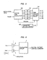
- Fig. 8 is a block diagram showing the configuration of the neutral voltage controller of the embodiment. As shown in Fig. 8, the neutral voltage controller of the embodiment is configured by a subtracter 1, two comparators 2, a calculation circuit 3, and insulation circuits 10.
- the subtracter 1 outputs a value which is obtained by subtracting the first reference voltage V ref1 from the neutral voltage V CN .
- the first reference voltage value V ref1 is one half (1/2•V PN ) of the voltage between the point P and the point N.
- a second reference voltage value V ref2 and a third reference voltage value V ref3 are used in addition to the first reference voltage value V ref1 .
- the second reference voltage value V ref2 and the third reference voltage value V ref3 are negative and positive values, respectively.
- One of the comparators 2 turns on a signal for raising the neutral voltage and outputs the signal to the calculation circuit 3 when the value of the output of the subtracter 1 is smaller than the second reference voltage value V ref2 .
- the other comparator 2 turns on a signal for lowering the neutral voltage V CN and outputs the signal to the calculation circuit 3 when the value of the output of the subtracter 1 is larger than the third reference voltage value V ref3 .
- the signals output from the two comparators 2 are input to the insulation circuits 10 as a 2-bit digital signal, and then input to the calculation circuit 3. Since the insulation circuits 10 are circuits which handle a digital signal, the circuits are not required to have a linear characteristic and the like in a wide range. Therefore, the insulation circuits can be configured more economically than the isolation amplifiers 6 shown in Fig. 2.
- the calculation circuit 3 receives the outputs of the two comparators 2. When the signals from the two comparators 2 are not input, the circuit maintains the neutral voltage as it is. When the signal for raising the neutral voltage is input, the circuit produces a neutral voltage control command for raising the neutral voltage. When the signal for lowering the neutral voltage is input, the circuit produces a neutral voltage control command for lowering the neutral voltage.
- the neutral voltage controller of the embodiment the differences between the neutral voltage V CN and the reference voltage values are converted from the analog signals to a digital signal. Therefore, the economical insulation circuits 10 which handle a digital signal can be used without using expensive insulation circuits having a wide linear characteristic. As a result, the whole apparatus can be economically configured.
- the differences between the neutral voltage V CN and the reference voltage values are processed in the form of a digital signal instead of an analog signal. Therefore, an influence of noises on the input to the calculation circuit 3 can be reduced, so that the reliability of the apparatus can be enhanced, and a highly accurate neutral voltage control is enabled.
- a dead band is disposed with using the second reference voltage value V ref2 and the third reference voltage value V ref3 as thresholds, thereby allowing the neutral voltage control to be performed without being affected by noises of a small level which are contained in the neutral voltage.
- the influence of noises can be eliminated, and a usual variation component, i.e., a variation component of a frequency which is thrice the operation frequency can be neglected. Therefore, simplification and high reliability of the control can be realized.
- the calculation circuit 3 may be configured by software, or by hardware such as an electric circuit.
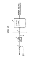
- Fig. 10 is a block diagram showing the configuration of the neutral voltage controller of the embodiment.
- the neutral voltage controller of the embodiment is different from the neutral voltage controller of the above-described embodiment in that the controller comprises a comparator 4 in place of the two comparators 2, and a storage device 5 instead of the calculation circuit 3.
- the comparator 4 receives a value which is obtained by subtracting the first reference voltage V ref1 from the neutral voltage V CN , and outputs three 2-bit digital signals which have different values in cases where the value of the output of the subtracter 1 is smaller than the second reference voltage value V ref2 , where the output value is equal to or larger than the second reference voltage value V ref2 and equal to or smaller than the third reference voltage value V ref3 , and where the output value is larger than the third reference voltage value V ref3 .
- the storage device 5 stores a plurality of tables of sets of values of the digital signals and neutral voltage control commands which are to be output at the values, in accordance with a motoring/regenerative operation of the inverter, or the operation status of the inverter according to the use status.
- the storage device 5 selects a table according to the present operation status, from the tables, and outputs a neutral voltage control command corresponding to a digital signal, with using the table.
- Table 2 shows switching states and changes of the neutral voltage.
- the switching states are switching patterns in the case where a vector is to be output, such as shown in Fig. 4, and indicated in the sequence of the U-, V-, and W-phases.
- P indicates a state where the phase is connected to point P on the positive side
- N indicates a state where the phase is connected to point N on the negative side
- O indicates a state where the phase is connected to neutral point C.
- ap vector and an vector are equivalent to each other as a line voltage to be output, but are different in switching state.
- a change of the neutral voltage in a motoring operation for example, the change in the case of ap vector is rising, and that in the case of an vector is lowering, or the changes are opposite to each other.
- the changes of the neutral voltage are opposite to each other. In this way, there are sets of voltage vectors in which, even when the line voltage to be output is identical, the neutral voltage can be raised or lowered. Depending on which vector is selected, therefore, the neutral voltage can be controlled.
Landscapes
- Engineering & Computer Science (AREA)
- Power Engineering (AREA)
- Inverter Devices (AREA)
Abstract
On the basis of: a first calculated value ic which is a
product of a calculated value of a time of three-phase output
voltages in a state where a positive bus, a negative bus, and
a neutral line are connected respectively to three-phase phase
output terminals, and a predicted neutral current value in the
state; and second and third calculated values icx and icy
which are products of a calculated value of a time of the
three-phase output voltages that can take state 1 where two of
the three-phase phase output terminals are connected to the
positive bus or the neutral line, and a remaining one terminal
is connected to the neutral line or the negative bus, and
state 2 opposite to the state, and predicted neutral current
values in states 1 and 2, a time ratio of state 1 and 2 during
a PWM period is determined so as to make a current flowing
through the neutral line close to zero, or a potential of the
neutral line of the three-phase output voltages close to a
voltage which is exactly the middle between voltages of the
positive and negative busses.
Description
The present invention relates to a three-level neutral-point-clamped
PWM inverter apparatus which is one of a power
converter such as an inverter or a servo drive that speed-variably
drives a motor, and a power converter that
interconnects systems, and also to a neutral voltage
controller which is used in such a three-level neutral-point-clamped
PWM inverter to control a neutral voltage that is a
voltage between a neutral point of two capacitors connected in
series between positive and negative busses of the apparatus,
and the negative bus.
Fig. 1 is a circuit diagram showing the main circuit
configuration of a three-level neutral-point-clamped PWM
inverter apparatus. As shown in Fig. 1, the three-level
neutral-point-clamped PWM inverter apparatus is configured by
two capacitors 7, three-phase output terminals, twelve
switching elements 8, and eighteen diodes 9.
In the thus configured three-level neutral-point-clamped
PWM inverter apparatus, when switching elements 81, 82 are
turned on, the output terminals of the phases are connected to
a positive bus which is connected to a point P, and output
phase voltages of the phases are at a high level. When
switching elements 82, 83 are turned on, the output terminals
of the phases are connected to a point C which is the neutral
point, and the output phase voltages of the phases are at an
intermediate level (neutral voltage) which is between the high
level and a low level. When switching elements 83, 84 are
turned on, the output terminals of the phases are connected to
a negative bus which is connected to a point N, and the output
phase voltages of the phases are at the low level. In the
three-level neutral-point-clamped PWM inverter apparatus,
usually, the switching elements 8 are switched on the basis of
the above-mentioned three patterns to drive a three-phase
load.
In such a three-level neutral-point-clamped PWM inverter
apparatus, the neutral voltage is obtained by voltage division
of the capacitors 7. The neutral voltage is varied in
accordance with a current supplied to the load. When the
neutral voltage is varied, an excess voltage is applied to the
capacitors 7, thereby causing the possibility that the
capacitors 7 are shortened in life or broken. In a three-level
neutral-point-clamped PWM inverter apparatus, therefore,
a neutral voltage control is performed in order to suppress or
control variation of the neutral voltage.
In a neutral voltage control of the thus configured
neutral-point-clamped PWM inverter, conventionally, the
current flowing through the neutral line is controlled by
using dipolar modulation or unipolar modulation as a method of
generating PWM pulses, and increasing and decreasing the zero-sequence
voltage of a voltage command.
On the other hand, as disclosed in JP-A-5-292754, when
the concept of a voltage vector is introduced and a PWM
control is performed, a method is usually employed in which a
neutral voltage control is performed while the increasing or
decreasing direction of an intermediate voltage vector is
determined from the sign of a load power. As proposed in JP-A-2001-57784,
such a method includes that in which a
generation time ratio of a correction vector is finely
adjusted in accordance with the direction of a current flowing
through a neutral line.
In these methods, variation of the neutral voltage is
suppressed by, among twelve sets of switch states such as
shown in Fig. 2, adjusting the ratio of paired switch states
in which the output voltages are equal to each other but the
current directions of the neutral line are opposite to each
other.
As proposed in JP-A-2001-61283, there is also a method
such as shown in Fig. 3 in which a switch state disturbing the
neutral voltage is suppressed. When switch states which can
be attained by a neutral-point-clamped PWM inverter are
indicated in the form of output voltage vectors, they can be
expressed as shown in Fig. 4.
Fig. 5 shows an example of an apparatus which calculates
a PWM pulse of a neutral-point-clamped PWM inverter with using
the concept of a space voltage vector. The apparatus
comprises a vector time calculator 102, a vector time register
103, a PWM pulse pattern setting device 104, and a parameter
setting device 105.
In the apparatus, it is assumed that an output voltage
output from the inverter is a space vector quantity such as
shown in Fig. 4. When the modulation rate (k) and phase ()
of an output voltage V are given, the vector time calculator
102 outputs the region of the output voltage vector V to the
PWM pulse pattern setting device 104, selects the 27 kinds of
vectors shown in Fig. 4, and calculates vector sequences which
are sequentially output and vector output times (TO - T5) as
PWM pulses in which an average of PWM periods is equal to the
output voltage vector V. The vector sequences and the vector
output times (TO - T5) are stored in the vector time register
103. The vector sequences and vector output times which are
stored are converted by the PWM pulse pattern setting device
104 to a pulse sequence of U1, U2, V1, V2, W1, and W2 which
drive switch elements of an inverter main circuit. The switch
elements of the inverter main circuit are turned on/off by the
pulse sequence, and a desired voltage is output. In this
apparatus, on the basis of the neutral voltage from the
parameter setting device 105 and a signal from a detector for
a load power factor, the PWM pulse pattern setting device 104
adjusts the generation time of the correction vector in a
direction along which the variation of the neutral voltage is
reduced.
JP-A-9-37592 discloses a method of PWM controlling a
three-level inverter in which a region between one long vector
of output space vectors of a three-level inverter, and a
vector that is adjacent to the long vector, and that has an
intermediate length is set as one space. The whole space of
360° which is formed by these vectors is divided into twelve
regions. The region number of a command vector in the twelve
regions is judged depending on the rotation angle of the
command vector. The modulation rate is calculated in
accordance with the degree of the command vector. The
transmission system and the transmission sequence for
suppressing variation of the neutral voltage of voltage
dividing capacitors of the three-level inverter are determined
in accordance with the modulation rate and the current ratio.
Specific output times of the vectors in the transmission
system and the transmission sequence are calculated to PWM
control the three-level inverter.
As described above, in a three-phase neutral-point-clamped
PWM inverter, usually, an even number of capacitors
are directly connected between positive and negative busses of
a main circuit in order to obtain the neutral voltage, and a
neutral line is used while being taken out from a capacitor
terminal which has a voltage that is exactly the middle
voltage between the positive and negative busses. The neutral
line is connected as shown in Figs. 2 and 3 depending on the
output load of the PWM inverter and the switch states of the
PWM inverter. The voltage of the neutral line (the neutral
voltage) is varied in accordance with the current which
charges the capacitors through the positive and negative
busses, and that which is supplied from the connected load.
As shown in the conventional art examples, in the switch
states shown in Fig. 3 (in the description, the vector is
referred to as a correction vector), a set of switch states in
which the line voltage to be output to the load is the same
but the phase of the load connected to the neutral line is
different (adjacent switch states in Fig. 2 are bundled into
one set) is used, and the time ratio in which the switch
states of the set are generated is adjusted, whereby the
neutral potential can be finely controlled.
In the switch states shown in Fig. 2 (in the description,
the vector is referred to as an intermediate vector), however,
the neutral voltage is varied by the phase currents of the
load connected to the neutral line and the time ratio in which
the switch state is generated, and there is no vector which
corrects the variation. Therefore, the variation of the
neutral voltage caused by an intermediate vector must be
corrected with using a correction vector.
As shown in JP-A-2-261063, therefore, a zero-sequence
voltage is added to the modulation rate, the occurrence time
of a correction vector is adjusted, and the variation of the
neutral voltage is controlled without changing the output line
voltage which is to be supplied to a load. As shown in JP-A-5-292754
and JP-A-2001-57784, also in the method which uses
the concept of a space voltage vector, an output is conducted
so that a correction vector is used in a voltage vector to be
used, and the occurrence time of the switch state of the set
is adjusted to control the neutral voltage. In these methods,
however, the technique of determining the ratio of the
correction vector to make the neutral voltage variation close
to zero is not optimum, and the effect of suppressing the
neutral voltage variation is insufficient.
In the method described in JP-A-9-37592, the transmission
system and the transmission sequence for suppressing variation
of the neutral potential of the voltage dividing capacitors of
the predetermined three-level inverter are determined in
accordance with the modulation rate and the current ratio, and
specific output times of the vectors in the transmission
system and the transmission sequence are calculated to perform
a PWM control. Therefore, it is possible to bring the neutral
current close to zero. In the method also, however, the
neutral voltage variation cannot be reduced completely to
zero.
Fig. 6 is a block diagram showing the configuration of a
conventional neutral voltage controller which detects the
level of the neutral voltage and outputs a neutral voltage
control command for suppressing the neutral voltage variation.
As shown in Fig. 6, the conventional neutral voltage
controller is configured by two isolation amplifiers 6 and a
calculation circuit 3.
A first reference voltage Vref1 which is one half of a
voltage VPN (DC bus voltage) between the point P and the point
N, and a voltage between the point C and the point N, i.e.,
the neutral voltage VCN are input to the two isolation
amplifiers 6, respectively. The calculation circuit 3
receives outputs of the two isolation amplifiers 6, calculates
a neutral voltage control command for making the neutral
voltage VCN and the first reference voltage Vref1 coincident
with each other, and outputs the command. The neutral voltage
control command is a command to produce an output pattern of a
PWM (Pulse Width Modulation) command for raising or lowering
the value of the neutral voltage.
As described above, in the neutral voltage controller,
the neutral voltage VCN and the first reference voltage Vref1
are input to the calculation circuit 3, and hence the two
isolation amplifiers 6 serving as insulation circuits are
required. Such insulation circuits are required because the
calculation circuit 3 is usually driven by a power source
which is different from that for the main circuit of the
inverter.
However, the isolation amplifiers 6 are expensive analog
insulation circuits having a wide linear characteristic, and
therefore have a problem in that the neutral voltage
controller is expensive. In the conventional neutral voltage
controller, since the calculation circuit 3 controls the
neutral voltage on the basis of analog signals, there is a
problem in that the apparatus is easily affected by noises or
the like.
It is an object of the invention to provide a three-phase
neutral-point-clamped PWM inverter apparatus in which the
neutral potential variation can be efficiently suppressed, and
the safety and the quality of the output voltage can be
improved.
In order to attain the object, in the three-phase
neutral-point-clamped PWM inverter apparatus of the invention,
a first calculated value which is a product of: a calculated
value of a time of three-phase output voltages in a state
where a positive bus, a negative bus, and a neutral line are
connected respectively to three-phase phase output terminals;
and a predicted neutral current value in the state is
obtained. Moreover, second and third calculated values which
are products of: a calculated value of a time of the three-phase
output voltages that can take state 1 where two of the
three-phase phase output terminals are connected to the
positive bus or the neutral line, and a remaining one terminal
is connected to the neutral line or the negative bus, and
state 2 opposite to the state; and predicted neutral current
values in states 1 and 2 are obtained. Furthermore, on the
basis of the first, second, and third calculated values, a
time ratio of state 1 and 2 during a PWM period is determined
so as to make a current flowing through the neutral line close
to zero, or a potential of the neutral line of the three-phase
output voltages close to a potential which is exactly the
middle between voltages of the positive and negative busses.
According to the configuration, the neutral potential
variation can be efficiently suppressed by making close to
zero as far as possible, or making the potential of the
neutral line close to a potential which is exactly the middle
between the potentials of the positive and negative busses.
Therefore, the safety and the quality of the output voltage
can be improved.
It is another object of the invention to provide a
neutral voltage controller which is economical, and highly
reliable and accurate.
In order to attain the object, in the invention, a first
reference voltage value which is one half of a voltage between
a positive bus and a negative bus is subtracted from a value
of a neutral voltage, when a result of the subtraction is
smaller than a second reference voltage value which is a
negative value, a signal for raising the neutral voltage is
turned on, when the result of the subtraction is larger than a
third reference voltage value which is a positive value, a
signal for lowering the neutral voltage is turned on, the two
signals are converted in an insulative manner to a 2-bit
digital signal, and a neutral voltage control command is
calculated on the basis of the digital signal and then output.
According to the configuration, the differences between
the neutral voltage and the reference voltage values are
expressed by a digital signal instead of an analog signal,
thereby enabling economical insulating means to be used
without using expensive insulating means having a wide linear
characteristic. Therefore, the whole apparatus can be
economically configured. Since the differences between the
neutral voltage and the reference voltage values are processed
in the form of a digital signal instead of an analog signal,
an influence of noises on an input to calculating means can be
reduced. Therefore, it is possible to provide a neutral
voltage controller in which the reliability is enhanced, and
which is highly accurate.
Hereinafter, preferred embodiments of the invention will
be described with reference to the drawings. In the drawings,
the same reference numerals denote the identical components.
Next, a three-phase neutral-point-clamped PWM inverter
apparatus of a first embodiment of the invention will be
described with reference to Fig. 7. Fig. 7 is a block diagram
showing the configuration of a PWM pulse calculator of a
three-phase neutral-point-clamped inverter apparatus of the
embodiment. As shown in Fig. 7, the three-phase neutral-point-clamped
inverter apparatus of the embodiment comprises a
neutral potential control parameter calculator 101, a vector
time calculator 102, a vector time register 103, and a PWM
pattern setting device 104.
When the three-phase neutral-point-clamped inverter
apparatus of the embodiment is to output an output voltage
vector V, PWM pulses are output on the basis of vectors
constituting the regions (regions 1 to 6) where the output
voltage vector V exists, shown in Fig. 4. Assuming that the
vectors constituting the regions are sorted as shown in Fig. 4,
the vector time calculator 102 calculates total output times
of the sorted vectors to output the output voltage vector V,
as follows:
- neutral current due to output of z vector : ic
- neutral current due to output of xp and xn vectors : icx
- neutral current due to output of yp and yn vectors : icy.
When the neutral currents ic, icx, and icy are obtained
in this way, the neutral potential variation can be made close
to zero by determining the time ratios of xp and xn, and yp
and yn vectors so that the current variation of the neutral
line is made close to zero by using ic, icx, and icy.
Hereinafter, an example of a specific method of
calculating the time ratios of the vectors will be described.
As described in JP-A-2001-57784, the parameter setting
device 105 uses neutral potential control parameters α, α1,
and α2 in the neutral potential control. Relationships among
the parameters are changed depending on relationships between
the region where the voltage vector exists and the phase
currents in the following manner:
Table 1 below shows the correspondence among phase1,
phase2, and phase3, and the U-, V-, and W-phases.
(Table 1)
Correspondence Table of Phases
| Region | phase1 | phase2 | phase3 |
| 1 | U | V | W |
| 2 | V | U | W |
| 3 | V | W | U |
| 4 | W | V | U |
| 5 | W | U | V |
| 6 | U | W | V |
Then, the time allocations of xp and xn vectors are set
as follows:
time of xp vector : Txp = α1 × T2
time of xn vector : Txn = (1 - α1) × T2,
and the time allocations of yp and yn vectors are set as
follows:
time of yp vector : Typ = α2 × T3
time of yn vector : Tyn = (1 - α2) × T3.
The neutral potential control parameter α is calculated
by a neutral potential control parameter calculator 106 as a
sum of two parameters α' and α" as follows:
α = α' + α" (0 ≤ α ≤ 1).
It is assumed that α is limited to a range of 0 or more to 1
or less.
Here, α' is calculated in the following manner:
D = γ/ (2 × β)
α' = D (when ic ≥ 0)
α' = -D (when ic < 0)
(also α' is limited to a range of 0 or more to 1 or less).
Furthermore, α" is an offset adjustment parameter, and
assumed to be used for compulsively controlling the neutral
potential in the case of an abnormal neutral potential or the
like, and to be usually 0.5.
Moreover, β and γ are obtained in the manner shown in (1)
to (4) below.
when icx and ic have the same sign,
when icx and ic have the same sign,
when icx and ic have the same sign,
When the neutral potential control parameter α is
calculated in this way, the neutral potential variation due to
the neutral current which is caused to flow by z vector can be
made close to zero as far as possible for each PWM period, by
efficiently using the neutral current which is caused to flow
by xp, xn, yp, and yn vectors.
Also in the method in which generation of z vector is
suppressed as in the method described in JP-A-2001-061283,
when T2 in the above calculation is set as the time elapsed
after generation of the vector is suppressed, the neutral
potential variation can be efficiently suppressed while
maintaining the above calculation as it is.
In the three-phase neutral-point-clamped PWM inverter
apparatus of the embodiment, in consideration of the case
where ic is so large that compensation cannot be completely
attained during the PWM period depending on the operation
conditions of the inverter, such as the case of |icx| + |icy|
≤ |ic|, compensation is performed in a slightly excessive
degree when
|icx| + |icy| ≥ |ic|, |icx| ≥ |ic|, and |icy| ≥ |ic|
are caused.
In order to realize the above, in the three-phase
neutral-point-clamped PWM inverter apparatus of the embodiment,
a change may be made so as to compensate the integral value of
a current which has flown through the neutral line up to now,
instead of compensation of the neutral current which is caused
to flow by z vector during a PWM period. Specifically, a
change may be made so that ic uses a sum of a time integral
value ic0 of a neutral current which has flown before the
previous period, and the neutral current i(phase2) caused by z
vector in the next PWM period, as indicated by the following
expression:
ic = ic0 + i(phase2) × T2.
According to the configuration, it is possible to
suppress the neutral potential variation which has not been
sufficiently suppressed during one period. The time integral
value ic0 of the neutral current may be measured by a current
sensor disposed on the neutral line, or calculated by
prediction based on the phase output currents coupled to the
neutral line.
In the case where the capacitances of series-connected
smoothing capacitors are equal to one another, when the
neutral current is made close to zero as in the three-phase
neutral-point-clamped PWM inverter apparatus of the embodiment,
the neutral potential variation can be made zero, and the
neutral potential can be controlled to the potential (the
potential is indicated by V0) which is exactly the middle
between the potentials of the positive and negative busses.
In the case where the capacitances of the series-connected
capacitors are made different from one another as a result of
deterioration with time, even when the neutral current is made
close to zero, however, the neutral potential cannot be
controlled to become the potential which is exactly the middle
between the potentials of the positive and negative busses.
In the invention, therefore, instead that the neutral
current is made close to zero from the calculated values of ic,
icx, and icy, the neutral current may be controlled so that
the currently is conversely increased so as to be close to V0.
In this case, the neutral potential control parameter
calculator 101 detects the level of the neutral potential. If
the potential is higher than V0, the neutral current can be
increased from the calculated values of ic, icx, and icy in
the direction of the arrow in Fig. 1, and, if the potential is
lower than V0, the neutral current can be increased in the
direction opposite to that of the arrow in Fig. 1.
The second neutral voltage controller of the invention
will be described. Fig. 8 is a block diagram showing the
configuration of the neutral voltage controller of the
embodiment. As shown in Fig. 8, the neutral voltage
controller of the embodiment is configured by a subtracter 1,
two comparators 2, a calculation circuit 3, and insulation
circuits 10.
The subtracter 1 outputs a value which is obtained by
subtracting the first reference voltage Vref1 from the neutral
voltage VCN. As described above, the first reference voltage
value Vref1 is one half (1/2•VPN) of the voltage between the
point P and the point N.
In the neutral voltage controller of the embodiment, in
addition to the first reference voltage value Vref1, a second
reference voltage value Vref2 and a third reference voltage
value Vref3 are used. As shown in Fig. 9, the second reference
voltage value Vref2 and the third reference voltage value Vref3
are negative and positive values, respectively.
One of the comparators 2 turns on a signal for raising
the neutral voltage and outputs the signal to the calculation
circuit 3 when the value of the output of the subtracter 1 is
smaller than the second reference voltage value Vref2. The
other comparator 2 turns on a signal for lowering the neutral
voltage VCN and outputs the signal to the calculation circuit 3
when the value of the output of the subtracter 1 is larger
than the third reference voltage value Vref3.
The signals output from the two comparators 2 are input
to the insulation circuits 10 as a 2-bit digital signal, and
then input to the calculation circuit 3. Since the insulation
circuits 10 are circuits which handle a digital signal, the
circuits are not required to have a linear characteristic and
the like in a wide range. Therefore, the insulation circuits
can be configured more economically than the isolation
amplifiers 6 shown in Fig. 2.
The calculation circuit 3 receives the outputs of the two
comparators 2. When the signals from the two comparators 2
are not input, the circuit maintains the neutral voltage as it
is. When the signal for raising the neutral voltage is input,
the circuit produces a neutral voltage control command for
raising the neutral voltage. When the signal for lowering the
neutral voltage is input, the circuit produces a neutral
voltage control command for lowering the neutral voltage.
As described above, in the neutral voltage controller of
the embodiment, the differences between the neutral voltage VCN
and the reference voltage values are converted from the analog
signals to a digital signal. Therefore, the economical
insulation circuits 10 which handle a digital signal can be
used without using expensive insulation circuits having a wide
linear characteristic. As a result, the whole apparatus can
be economically configured.
In the neutral voltage controller of the embodiment, the
differences between the neutral voltage VCN and the reference
voltage values are processed in the form of a digital signal
instead of an analog signal. Therefore, an influence of
noises on the input to the calculation circuit 3 can be
reduced, so that the reliability of the apparatus can be
enhanced, and a highly accurate neutral voltage control is
enabled.
In the neutral voltage controller of the embodiment, a
dead band is disposed with using the second reference voltage
value Vref2 and the third reference voltage value Vref3 as
thresholds, thereby allowing the neutral voltage control to be
performed without being affected by noises of a small level
which are contained in the neutral voltage. In the neutral
voltage controller of the embodiment, moreover, it is
preferable to set the thresholds due to the second reference
voltage value Vref2 and the third reference voltage value Vref3
so as to be wider the neutral voltage variation which occurs
at a frequency that is three times the frequency output by the
three-level inverter apparatus. According to the
configuration, the influence of noises can be eliminated, and
a usual variation component, i.e., a variation component of a
frequency which is thrice the operation frequency can be
neglected. Therefore, simplification and high reliability of
the control can be realized. The calculation circuit 3 may be
configured by software, or by hardware such as an electric
circuit.
Next, a neutral voltage controller of a third embodiment
of the invention will be described with reference to Fig. 10.
Fig. 10 is a block diagram showing the configuration of the
neutral voltage controller of the embodiment. As shown in Fig.
10, the neutral voltage controller of the embodiment is
different from the neutral voltage controller of the above-described
embodiment in that the controller comprises a
comparator 4 in place of the two comparators 2, and a storage
device 5 instead of the calculation circuit 3.
The comparator 4 receives a value which is obtained by
subtracting the first reference voltage Vref1 from the neutral
voltage VCN, and outputs three 2-bit digital signals which have
different values in cases where the value of the output of the
subtracter 1 is smaller than the second reference voltage
value Vref2, where the output value is equal to or larger than
the second reference voltage value Vref2 and equal to or smaller
than the third reference voltage value Vref3, and where the
output value is larger than the third reference voltage value
Vref3.
The storage device 5 stores a plurality of tables of sets
of values of the digital signals and neutral voltage control
commands which are to be output at the values, in accordance
with a motoring/regenerative operation of the inverter, or the
operation status of the inverter according to the use status.
The storage device 5 selects a table according to the present
operation status, from the tables, and outputs a neutral
voltage control command corresponding to a digital signal,
with using the table.
Table 2 shows switching states and changes of the neutral
voltage. The switching states are switching patterns in the
case where a vector is to be output, such as shown in Fig. 4,
and indicated in the sequence of the U-, V-, and W-phases. P
indicates a state where the phase is connected to point P on
the positive side, N indicates a state where the phase is
connected to point N on the negative side, and O indicates a
state where the phase is connected to neutral point C.
As apparent from Fig. 4, for example, ap vector and an
vector are equivalent to each other as a line voltage to be
output, but are different in switching state. With respect to
a change of the neutral voltage in a motoring operation, for
example, the change in the case of ap vector is rising, and
that in the case of an vector is lowering, or the changes are
opposite to each other. Also in motoring and regenerative
operations, the changes of the neutral voltage are opposite to
each other. In this way, there are sets of voltage vectors in
which, even when the line voltage to be output is identical,
the neutral voltage can be raised or lowered. Depending on
which vector is selected, therefore, the neutral voltage can
be controlled. In the neutral voltage controller of the
embodiment, these relationships are stored in form of a table,
so that, with respect to variation of the neutral voltage, a
pattern which cancels the variation can be selected.
| Voltage vector | Switching state | Change of neutral voltage | |
| Motoring | Regenerative | ||
| Op | PPP | Unchanged | Unchanged |
| Oo | OOO | Unchanged | Unchanged |
| On | NNN | Unchanged | Unchanged |
| a | PNN,NPN,NNP | Unchanged | Unchanged |
| b | PPN,NPP,PNP | Unchanged | Unchanged |
| c | PON,OPN,NPO, | Depending | Depending |
| NOP,ONP,PNO | on phase | on phase | |
| ap | POO,OPO,OOP | Raising | Lowering |
| bp | PPO,OPP,POP | Raising | Lowering |
| an | ONN,NON,NNO | Lowering | Raising |
| bn | OON,NOO,ONO | Lowering | Raising |
Claims (11)
- A three-phase neutral-point-clamped PWM inverter apparatus which has a positive bus, a negative bus, and a neutral line, and in which neutral-point-clamped PWM inverters for three phases are disposed, each of said neutral-point-clamped PWM inverters being configured by: connecting in series first and second switch elements, and third and fourth switch elements between said positive bus and a phase voltage output terminal, and said negative bus and a phase output terminal, respectively; and connecting a node between said first and second switch elements, and a node between said third and fourth switch elements to said neutral point via respective clamp elements, characterized in that said apparatus comprises:means for obtaining a first calculated value which is a product of: a calculated value of a time of three-phase output voltages in a state where said positive bus, said negative bus, and said neutral line are connected respectively to said three-phase phase output terminals during a PWM period; and a value of a current which is predicted to flow through said neutral point in said state;means for obtaining a second calculated value which is a products of: a calculated value of a time of three-phase output voltages that can take a second state where two of said three-phase phase output terminals are connected to said positive bus, and one of said three-phase phase output terminals is connected to said neutral line, or a third state where two of said three-phase phase output terminals are connected to said neutral line, and one of said three-phase phase output terminals is connected to said negative bus; and a value of a current which is predicted to flow through said neutral line in said state;means for obtaining a third calculated value which is a products of: a calculated value of a time of three-phase output voltages that can take a fourth state where one of said three-phase phase output terminals is connected to said positive bus, and two of said three-phase phase output terminals are connected to said neutral line, or a fifth state where one of said three-phase phase output terminals is connected to said neutral line, and two of said three-phase phase output terminals are connected to said negative bus; and a value of a current which is predicted to flow through said neutral line in said state; andratio determining means for determining ratios of said second and third states, and said fourth and fifth states during a PWM period so as to, on the basis of said first, second, and third calculated values, make a current flowing through said neutral line close to zero, or a potential of said neutral line close to a potential which is exactly a middle between potentials of said positive and negative busses.
- A three-phase neutral-point-clamped PWM inverter apparatus according to claim 1, wherein, in place of said ratio determining means set froth in claim 1, ratio determining means obtains a fourth calculated value which is a sum of said first calculated value, and an integral value of a current which has flown through said neutral line up to a PWM period preceding by one period, and determines ratios of said second and third states, and said fourth and fifth states during a PWM period so as to, on the basis of said second and third calculated values, make said fourth calculated value close to zero, or, with using said fourth calculated value, a potential of said neutral line close to a potential which is exactly a middle between potentials of said positive and negative busses.
- A three-phase neutral-point-clamped PWM inverter apparatus according to claim 1, wherein, in a three-phase neutral-point-clamped PWM inverter apparatus in which a time of three-phase output voltages in six switch states where said positive bus, said negative bus, and said neutral line are connected respectively to said three-phase phase output terminals is suppressed to a first preset value or smaller, and an insufficient amount of an output voltage is compensated six switch states where each of said three-phase phase output terminals is connected to said positive bus or said negative bus, and excluding a state where all of three of said three-phase phase output terminals are concurrently connected to said positive bus or said negative bus,
in place of said means for obtaining said first calculated value set froth in claim 1, means obtains a first calculated value which is a product of: the time of three-phase output voltages which are suppressed to said first preset value or smaller during a PWM period; and a value of a current which is predicted to flow through said neutral point in said state. - A three-phase neutral-point-clamped PWM inverter apparatus according to claim 3, wherein a measured value of a current flowing through said neural line is used in place of said current which is predicted to flow through said neutral point, and said ratio determining means obtains a fourth calculated value which is a sum of said first calculated value, and an integral value of a current which has flown through said neutral line up to a PWM period preceding by one period, and determines ratios of said second and third states, and said fourth and fifth states during a PWM period so as to, on the basis of said second and third calculated values, make said fourth calculated value close to zero, or, with using said fourth calculated value, a potential of said neutral line close to a potential which is exactly a middle between potentials of said positive and negative busses.
- A three-phase neutral-point-clamped PWM inverter apparatus according to any one of claims 1 to 3, wherein, in said means for obtaining said first to third calculated values, said value of said current which is predicted to flow through said neutral point is calculated by using a value of a current which is predicted to flow through said phase output terminal connected to said neutral line.
- A neutral voltage controller which controls a neutral voltage that is a voltage between a neutral point of two capacitors connected in series between positive and negative busses of a three-level inverter apparatus, and said negative bus, characterized in that said neutral voltage controller comprises:subtracting means for outputting a value which is obtained by subtracting a first reference voltage value from a value of said neutral voltage, said first reference voltage value being one half of a voltage between said positive and negative busses;first comparing means for, when said value output from said subtracting means is smaller than a second reference voltage value which is a negative value, turning on a signal for raising said neutral voltage;second comparing means for, when said value output from said subtracting means is larger than a third reference voltage value which is a positive value, turning on a signal for lowering said neutral voltage;insulating means for converting said two signals to a 2-bit digital signal in an insulative manner; andcalculating means for, on the basis of said digital signal, calculating a neutral voltage control command, and outputting said command.
- A neutral voltage controller which controls a neutral voltage that is a voltage between a neutral point of two capacitors connected in series between positive and negative busses of a three-level inverter apparatus, and said negative bus, characterized in that said neutral voltage controller comprises:subtracting means for outputting a value which is obtained by subtracting a first reference voltage value from a value of said neutral voltage, said first reference voltage value being one half of a voltage between said positive and negative busses;a comparator which outputs a 2-bit digital signal having different values in cases where said value output from said subtracting means is smaller than a second reference voltage value which is a negative value, where said value output from said subtracting means is larger than a third reference voltage value which is a positive value, and where said value output from said subtracting means is equal to or larger than said second reference voltage value and equal to or smaller than said third reference voltage value;insulating means for outputting said bit digital signal in an insulative manner; andcalculating means for, on the basis of said digital signal, calculating a neutral voltage control command, and outputting said command.
- A neutral voltage controller which controls a neutral voltage that is a voltage between a neutral point of two capacitors connected in series between positive and negative busses of a three-level inverter apparatus, and said negative bus, characterized in that said neutral voltage controller comprises:subtracting means for outputting a value which is obtained by subtracting a first reference voltage value from a value of said neutral voltage, said first reference voltage value being one half of a voltage between said positive and negative busses;first comparing means for, when said value output from said subtracting means is smaller than a second reference voltage value which is a negative value, turning on a signal for raising said neutral voltage;second comparing means for, when said value output from said subtracting means is larger than a third reference voltage value which is a positive value, turning on a signal for lowering said neutral voltage;insulating means for converting said two signals in an insulative manner to a 2-bit digital signal; andstorage means for previously storing a table of sets of a value of said digital signal and a neutral voltage control command which is to be output at said value, obtaining a neutral voltage control command which corresponds to said digital signal supplied from said insulating means, from said table, and outputting said neutral voltage control command.
- A neutral voltage controller which controls a neutral voltage that is a voltage between a neutral point of two capacitors connected in series between positive and negative busses of a three-level inverter apparatus, and said negative bus, characterized in that said neutral voltage controller comprises:subtracting means for outputting a value which is obtained by subtracting a first reference voltage value from a value of said neutral voltage, said first reference voltage value being one half of a voltage between said positive and negative busses;a comparator which outputs a 2-bit digital signal having different values in cases where said value output from said subtracting means is smaller than a second reference voltage value which is a negative value, where said value output from said subtracting means is larger than a third reference voltage value which is a positive value, and where said value output from said subtracting means is equal to or larger than said second reference voltage value and equal to or smaller than said third reference voltage value;insulating means for outputting said digital signal in an insulative manner; andstorage means for previously storing a table of sets of a value of said digital signal and a neutral voltage control command which is to be output at said value, obtaining a neutral voltage control command which corresponds to said digital signal supplied from said insulating means, from said table, and outputting said neutral voltage control command.
- A neutral voltage controller according to claim 9, wherein said storage means stores a plurality of said tables corresponding to operation statuses of an inverter, selects a table corresponding to a present operation status, from said tables, and outputs a neutral voltage control command corresponding to said digital signal with using said table.
- A neutral voltage controller according to any one of claims 6 to 10, wherein a difference between said second and third reference voltage values is set to be larger than an amplitude of neutral voltage variation at a frequency which is three times an output frequency of said three-level inverter.
Applications Claiming Priority (5)
| Application Number | Priority Date | Filing Date | Title |
|---|---|---|---|
| JP2000372889A JP3695522B2 (en) | 2000-12-07 | 2000-12-07 | 3-level inverter device |
| JP2000372889 | 2000-12-07 | ||
| JP2000380915A JP3694763B2 (en) | 2000-12-14 | 2000-12-14 | Three-phase neutral point clamp type PWM inverter device |
| JP2000380915 | 2000-12-14 | ||
| PCT/JP2001/010480 WO2002050989A1 (en) | 2000-12-07 | 2001-11-30 | Three-level neutral point clamping pwm inverter and neutral point voltage controller |
Publications (2)
| Publication Number | Publication Date |
|---|---|
| EP1347565A1 true EP1347565A1 (en) | 2003-09-24 |
| EP1347565A4 EP1347565A4 (en) | 2007-03-14 |
Family
ID=26605422
Family Applications (1)
| Application Number | Title | Priority Date | Filing Date |
|---|---|---|---|
| EP01271687A Withdrawn EP1347565A4 (en) | 2000-12-07 | 2001-11-30 | PWM INVERTER TO NEUTRAL POINT WITH THREE LEVELS AND NEUTRAL POINT VOLTAGE CONTROL UNIT |
Country Status (6)
| Country | Link |
|---|---|
| US (1) | US6795323B2 (en) |
| EP (1) | EP1347565A4 (en) |
| KR (1) | KR100650358B1 (en) |
| CN (1) | CN100334801C (en) |
| TW (1) | TW546905B (en) |
| WO (1) | WO2002050989A1 (en) |
Cited By (3)
| Publication number | Priority date | Publication date | Assignee | Title |
|---|---|---|---|---|
| CN102937688A (en) * | 2012-10-30 | 2013-02-20 | 浙江万里学院 | Device open-circuit fault diagnosis circuit for diode neutral point clamped (NPC) three-level inverter |
| EP3116096A4 (en) * | 2014-03-04 | 2017-11-22 | Eaton Corporation | Ups circuit |
| EP2180589A3 (en) * | 2008-10-02 | 2018-02-07 | Samsung Electronics Co., Ltd. | Method to predict phase current |
Families Citing this family (54)
| Publication number | Priority date | Publication date | Assignee | Title |
|---|---|---|---|---|
| EP2045905B1 (en) * | 2001-09-29 | 2013-06-12 | Daikin Industries, Ltd. | Phase current detection method, inverter control method, motor control method, and apparatuses used in these methods |
| JP3864307B2 (en) * | 2002-06-12 | 2006-12-27 | 株式会社安川電機 | PWM inverter control device and control method |
| US6838925B1 (en) * | 2003-10-07 | 2005-01-04 | American Power Conversion Corporation | Three level inverter |
| US7164254B2 (en) * | 2005-02-28 | 2007-01-16 | Rockwell Automation Technologies, Inc. | Modulation methods and apparatus for reducing common mode voltages |
| US7190143B2 (en) * | 2005-05-27 | 2007-03-13 | Rockwell Automation Technologies, Inc. | Pulse width modulation (PWM) rectifier with variable switching frequency |
| FR2895598B1 (en) * | 2005-12-22 | 2008-09-05 | Valeo Equip Electr Moteur | METHOD FOR CONTROLLING A POLYPHASE VOLTAGE ONDULATOR |
| US7193388B1 (en) | 2006-02-02 | 2007-03-20 | Emerson Electric Co. | Offset PWM signals for multiphase motor |
| JP5474772B2 (en) * | 2007-06-01 | 2014-04-16 | ディーアールエス パワー アンド コントロール テクノロジーズ インコーポレーテッド | Three-level neutral point fixed conversion device and control method thereof |
| US20090016089A1 (en) * | 2007-07-09 | 2009-01-15 | Nguyen Vietson M | Electromechanical power transfer system with even phase number dynamoelectric machine and three level inverter |
| US7986535B2 (en) * | 2007-07-17 | 2011-07-26 | Raytheon Company | Methods and apparatus for a cascade converter using series resonant cells with zero voltage switching |
| US7839023B2 (en) * | 2007-07-18 | 2010-11-23 | Raytheon Company | Methods and apparatus for three-phase inverter with reduced energy storage |
| KR100928549B1 (en) * | 2007-11-30 | 2009-11-24 | 한국전기연구원 | Switch clamp multi-level inverter |
| EP2107672A1 (en) * | 2008-03-31 | 2009-10-07 | SMA Solar Technology AG | Three-phase inverter without connection between the neutral conductor of the grid and the mid-point of the intermediate circuit |
| CN100557943C (en) * | 2008-06-13 | 2009-11-04 | 株洲南车时代电气股份有限公司 | A Synchronous Modulation Method Based on Space Vector |
| KR101052275B1 (en) | 2009-02-28 | 2011-07-27 | 울산대학교 산학협력단 | Multi-Level Inverter PMM Generator Using FPA |
| FR2958815B1 (en) | 2010-04-07 | 2012-03-16 | Schneider Toshiba Inverter | METHOD FOR CONTROLLING AN INVERTER OF NPC TYPE |
| JP5126302B2 (en) | 2010-06-30 | 2013-01-23 | 株式会社安川電機 | 3-level inverter, power conditioner and power generation system |
| TWI404320B (en) * | 2010-06-30 | 2013-08-01 | Univ Nat Chiao Tung | A controller apparatus for controlling a dc/ac converter and method thereof |
| FR2962608B1 (en) * | 2010-07-07 | 2012-08-10 | Toulouse Inst Nat Polytech | NEW REDUNDANCY STRUCTURES FOR STATIC CONVERTERS |
| WO2012040257A1 (en) * | 2010-09-21 | 2012-03-29 | Curtiss-Wright Electro-Mechanical Corporation | Two terminal multilevel converter |
| CN102013824A (en) * | 2010-09-21 | 2011-04-13 | 深圳市大族激光科技股份有限公司 | Controller for inhibiting neutral point potential drift in three-level inverter |
| CN101976968B (en) * | 2010-09-25 | 2012-07-25 | 西安交通大学 | Method for controlling midpoint potential of direct-current bus of three-level inverter |
| JP5271327B2 (en) * | 2010-09-27 | 2013-08-21 | パナソニックEsパワーツール株式会社 | Electric tool |
| MX2013007362A (en) | 2010-12-22 | 2013-12-16 | Ge Energy Power Conversion Technology Ltd | CAPACITOR COMPENSATOR CIRCUIT AND CONTROL METHOD FOR AN ELECTRONIC DEVICE SUCH AS A MULTIPLE LEVEL POWER INVERTER. |
| CA2822593A1 (en) | 2010-12-22 | 2012-06-28 | Ge Energy Power Conversion Technology Limited | Mechanical arrangement of a multilevel power converter circuit |
| US8730691B2 (en) | 2011-05-11 | 2014-05-20 | Eaton Corporation | Power conversion apparatus and methods employing variable-level inverters |
| DE102012204721A1 (en) * | 2012-03-23 | 2013-09-26 | Schaeffler Technologies AG & Co. KG | Direct drive for a rotary machine, in particular for a container treatment machine |
| US8619446B2 (en) | 2012-04-27 | 2013-12-31 | Rockwell Automation Technologies, Inc. | Cascaded H-bridge (CHB) inverter level shift PWM with rotation |
| US9225262B2 (en) | 2012-06-29 | 2015-12-29 | Eaton Corporation | Multi-level inverter apparatus and methods using variable overcurrent response |
| CN102751882A (en) * | 2012-07-14 | 2012-10-24 | 张翔 | Three-phase neutral-point clamped four-quadrant operation three-level power supply conversion device |
| US9007787B2 (en) | 2012-08-13 | 2015-04-14 | Rockwell Automation Technologies, Inc. | Method and apparatus for bypassing Cascaded H-Bridge (CHB) power cells and power sub cell for multilevel inverter |
| US9425705B2 (en) | 2012-08-13 | 2016-08-23 | Rockwell Automation Technologies, Inc. | Method and apparatus for bypassing cascaded H-bridge (CHB) power cells and power sub cell for multilevel inverter |
| EP2891240A1 (en) * | 2012-08-28 | 2015-07-08 | ABB Technology AG | Controlling a modular converter in two stages |
| WO2014046555A1 (en) * | 2012-09-21 | 2014-03-27 | Auckland Uniservices Limited | Improvements in or relating to modular multi-level converters |
| EP2913915B1 (en) * | 2012-10-23 | 2018-08-01 | Mitsubishi Electric Corporation | Power conversion device |
| US9240731B2 (en) | 2013-03-18 | 2016-01-19 | Rockwell Automation Technologies, Inc. | Power cell bypass method and apparatus for multilevel inverter |
| CN103151946A (en) * | 2013-03-26 | 2013-06-12 | 上海交通大学 | A neutral-point clamped H-bridge five-level high-voltage frequency converter and its modulation method |
| US9083230B2 (en) | 2013-06-20 | 2015-07-14 | Rockwell Automation Technologies, Inc. | Multilevel voltage source converters and systems |
| US9397584B2 (en) | 2013-09-25 | 2016-07-19 | Eaton Corporation | Multi-level converter apparatus and methods using clamped node bias |
| US9520800B2 (en) | 2014-01-09 | 2016-12-13 | Rockwell Automation Technologies, Inc. | Multilevel converter systems and methods with reduced common mode voltage |
| US9325252B2 (en) | 2014-01-13 | 2016-04-26 | Rockwell Automation Technologies, Inc. | Multilevel converter systems and sinusoidal pulse width modulation methods |
| JP6176495B2 (en) * | 2014-08-19 | 2017-08-09 | 富士電機株式会社 | 3-level inverter control method and control apparatus |
| US9559541B2 (en) | 2015-01-15 | 2017-01-31 | Rockwell Automation Technologies, Inc. | Modular multilevel converter and charging circuit therefor |
| KR102352890B1 (en) | 2015-05-06 | 2022-01-19 | 삼성전자주식회사 | Dc-dc converter having circuits for controlling volatge of flying capacitor and therefore voltage controlling method |
| US9748862B2 (en) | 2015-05-13 | 2017-08-29 | Rockwell Automation Technologies, Inc. | Sparse matrix multilevel actively clamped power converter |
| US9742311B2 (en) | 2015-10-02 | 2017-08-22 | Hamilton Sundstrand Corporation | Systems and methods for controlling inverters |
| US9812990B1 (en) | 2016-09-26 | 2017-11-07 | Rockwell Automation Technologies, Inc. | Spare on demand power cells for modular multilevel power converter |
| CN118432460A (en) * | 2017-01-18 | 2024-08-02 | 钱利斌 | I/O timetable, manufacturing method and output method and equipment using same |
| US10158299B1 (en) | 2018-04-18 | 2018-12-18 | Rockwell Automation Technologies, Inc. | Common voltage reduction for active front end drives |
| CN109525134B (en) * | 2018-11-29 | 2020-11-27 | 北京科诺伟业科技股份有限公司 | Discontinuous PWM modulation method for diode clamping three-level inverter |
| US11211879B2 (en) | 2019-09-23 | 2021-12-28 | Rockwell Automation Technologies, Inc. | Capacitor size reduction and lifetime extension for cascaded H-bridge drives |
| US11444415B2 (en) | 2019-09-30 | 2022-09-13 | Eaton Intelligent Power Limited | Uninterruptible power supplies with replaceable receptacle panels and related methods |
| US11342878B1 (en) | 2021-04-09 | 2022-05-24 | Rockwell Automation Technologies, Inc. | Regenerative medium voltage drive (Cascaded H Bridge) with reduced number of sensors |
| CN117937965B (en) * | 2024-03-25 | 2024-06-04 | 西安图为电气技术有限公司 | Neutral point potential balance control method, electronic device, and computer-readable storage medium |
Family Cites Families (22)
| Publication number | Priority date | Publication date | Assignee | Title |
|---|---|---|---|---|
| JPS56115182A (en) * | 1980-02-15 | 1981-09-10 | Toshiba Corp | Inverter |
| US4670828A (en) * | 1986-02-25 | 1987-06-02 | Sundstrand Corporation | Bi-directional switch for neutral point clamped PWM inverter |
| JP2821168B2 (en) | 1989-03-31 | 1998-11-05 | 株式会社日立製作所 | Inverter device and AC motor drive system |
| EP0838855B1 (en) * | 1991-09-20 | 2004-11-24 | Hitachi, Ltd. | Semiconductor module |
| JP3229897B2 (en) | 1992-04-13 | 2001-11-19 | 三菱電機株式会社 | Three-level three-phase inverter device |
| JPH08317663A (en) * | 1995-05-15 | 1996-11-29 | Toshiba Corp | Neutral point clamp type power converter controller |
| JP3249380B2 (en) * | 1995-06-13 | 2002-01-21 | 株式会社東芝 | Power converter |
| JPH0937592A (en) | 1995-07-21 | 1997-02-07 | Toyo Electric Mfg Co Ltd | PWM control method and control device for three-level inverter |
| US5790396A (en) * | 1995-12-19 | 1998-08-04 | Kabushiki Kaisha Toshiba | Neutral point clamped (NPC) inverter control system |
| JP3226788B2 (en) * | 1996-05-10 | 2001-11-05 | 株式会社東芝 | Power converter |
| JP3263317B2 (en) * | 1996-06-18 | 2002-03-04 | 株式会社東芝 | Switching module and power converter using the module |
| US5684688A (en) * | 1996-06-24 | 1997-11-04 | Reliance Electric Industrial Company | Soft switching three-level inverter |
| JP3796881B2 (en) * | 1997-03-07 | 2006-07-12 | 神鋼電機株式会社 | 3-level inverter control method and apparatus |
| JPH11122944A (en) * | 1997-10-15 | 1999-04-30 | Toshiba Corp | Control device for NPC converter |
| US6058031A (en) | 1997-10-23 | 2000-05-02 | General Electric Company | Five level high power motor drive converter and control system |
| US5910892A (en) * | 1997-10-23 | 1999-06-08 | General Electric Company | High power motor drive converter system and modulation control |
| US5982646A (en) * | 1998-06-30 | 1999-11-09 | General Electric Company | Voltage clamp snubbers for three level converter |
| DE19829856A1 (en) * | 1998-07-02 | 2000-01-05 | Abb Research Ltd | Three-point converter and method of operation |
| JP3666557B2 (en) * | 1999-04-20 | 2005-06-29 | 富士電機機器制御株式会社 | Power conversion circuit |
| JP3745561B2 (en) * | 1999-06-28 | 2006-02-15 | 東芝三菱電機産業システム株式会社 | Multi-level neutral point potential fixed power converter |
| JP3841253B2 (en) | 1999-08-12 | 2006-11-01 | 株式会社安川電機 | Neutral point potential control method for neutral point clamp inverter |
| JP3841254B2 (en) | 1999-08-19 | 2006-11-01 | 株式会社安川電機 | Three-phase neutral point clamp type PWM inverter device |
-
2001
- 2001-11-30 CN CNB018201784A patent/CN100334801C/en not_active Expired - Fee Related
- 2001-11-30 EP EP01271687A patent/EP1347565A4/en not_active Withdrawn
- 2001-11-30 WO PCT/JP2001/010480 patent/WO2002050989A1/en not_active Ceased
- 2001-11-30 KR KR1020037007601A patent/KR100650358B1/en not_active Expired - Fee Related
- 2001-11-30 US US10/433,891 patent/US6795323B2/en not_active Expired - Lifetime
- 2001-12-05 TW TW090130172A patent/TW546905B/en not_active IP Right Cessation
Cited By (5)
| Publication number | Priority date | Publication date | Assignee | Title |
|---|---|---|---|---|
| EP2180589A3 (en) * | 2008-10-02 | 2018-02-07 | Samsung Electronics Co., Ltd. | Method to predict phase current |
| CN102937688A (en) * | 2012-10-30 | 2013-02-20 | 浙江万里学院 | Device open-circuit fault diagnosis circuit for diode neutral point clamped (NPC) three-level inverter |
| CN102937688B (en) * | 2012-10-30 | 2015-01-28 | 浙江万里学院 | Device open-circuit fault diagnosis circuit for diode neutral point clamped (NPC) three-level inverter |
| EP3116096A4 (en) * | 2014-03-04 | 2017-11-22 | Eaton Corporation | Ups circuit |
| US10536030B2 (en) | 2014-03-04 | 2020-01-14 | Eaton Intelligent Power Limited | UPS circuit |
Also Published As
| Publication number | Publication date |
|---|---|
| CN100334801C (en) | 2007-08-29 |
| EP1347565A4 (en) | 2007-03-14 |
| KR20030060980A (en) | 2003-07-16 |
| TW546905B (en) | 2003-08-11 |
| US6795323B2 (en) | 2004-09-21 |
| KR100650358B1 (en) | 2006-11-27 |
| WO2002050989A1 (en) | 2002-06-27 |
| CN1479963A (en) | 2004-03-03 |
| US20040057262A1 (en) | 2004-03-25 |
Similar Documents
| Publication | Publication Date | Title |
|---|---|---|
| US6795323B2 (en) | Three-level neutral point clamping pwn inverter and neutral point voltage controller | |
| US6751105B2 (en) | Method for controlling pwm pulse | |
| US6490185B1 (en) | Method for controlling neutral point potential of inverter of neutral point clamping type | |
| US9362840B2 (en) | Power conversion device | |
| US6337804B1 (en) | Multilevel PWM voltage source inverter control at low output frequencies | |
| US20130194852A1 (en) | Power converting appartatus | |
| US9001542B2 (en) | Current-source power converting apparatus | |
| JP3856689B2 (en) | Neutral point clamp type power converter controller | |
| US7183728B2 (en) | Motor drive system and process | |
| US10075093B2 (en) | Power conversion device for suppressing fluctuation of common mode voltage | |
| CN100466449C (en) | Neutral point voltage control device | |
| JP2018148595A (en) | Multilevel power conversion device and control method of the same | |
| CN119013885A (en) | Power conversion device | |
| JPH0937592A (en) | PWM control method and control device for three-level inverter | |
| JP3010005B2 (en) | Inverter device | |
| JP4448294B2 (en) | Power converter | |
| JP2005295625A (en) | Power converter | |
| JPH09149658A (en) | Series multiple inverter device | |
| CN112886839B (en) | Circulating current suppression method applied to three-level inverter | |
| JP2007097394A (en) | Power converter | |
| JP2022113486A (en) | Power supply device | |
| JPH09149657A (en) | Inverter device | |
| JP2002186263A (en) | Three-phase neutral point clamp type PWM inverter device | |
| JPH07170750A (en) | Inverter device | |
| JP2017079571A (en) | 3-level inverter control method and control apparatus |
Legal Events
| Date | Code | Title | Description |
|---|---|---|---|
| PUAI | Public reference made under article 153(3) epc to a published international application that has entered the european phase |
Free format text: ORIGINAL CODE: 0009012 |
|
| 17P | Request for examination filed |
Effective date: 20030606 |
|
| AK | Designated contracting states |
Kind code of ref document: A1 Designated state(s): AT BE CH CY DE DK ES FI FR GB GR IE IT LI LU MC NL PT SE TR |
|
| RBV | Designated contracting states (corrected) |
Designated state(s): AT BE DE GB |
|
| A4 | Supplementary search report drawn up and despatched |
Effective date: 20070214 |
|
| 17Q | First examination report despatched |
Effective date: 20090302 |
|
| STAA | Information on the status of an ep patent application or granted ep patent |
Free format text: STATUS: THE APPLICATION IS DEEMED TO BE WITHDRAWN |
|
| 18D | Application deemed to be withdrawn |
Effective date: 20160826 |