EP1347547B1 - Producing modulated light using electron emitters - Google Patents
Producing modulated light using electron emitters Download PDFInfo
- Publication number
- EP1347547B1 EP1347547B1 EP02024735A EP02024735A EP1347547B1 EP 1347547 B1 EP1347547 B1 EP 1347547B1 EP 02024735 A EP02024735 A EP 02024735A EP 02024735 A EP02024735 A EP 02024735A EP 1347547 B1 EP1347547 B1 EP 1347547B1
- Authority
- EP
- European Patent Office
- Prior art keywords
- light
- optical
- substrate
- electro
- electrical
- Prior art date
- Legal status (The legal status is an assumption and is not a legal conclusion. Google has not performed a legal analysis and makes no representation as to the accuracy of the status listed.)
- Expired - Lifetime
Links
- 239000000758 substrate Substances 0.000 claims description 74
- 230000003287 optical effect Effects 0.000 claims description 68
- 239000000463 material Substances 0.000 claims description 22
- 238000004519 manufacturing process Methods 0.000 claims description 17
- 238000000034 method Methods 0.000 claims description 17
- 239000004065 semiconductor Substances 0.000 claims description 6
- 229910052710 silicon Inorganic materials 0.000 claims description 5
- 239000010703 silicon Substances 0.000 claims description 5
- 230000008569 process Effects 0.000 claims description 4
- 239000010409 thin film Substances 0.000 claims description 3
- 230000005540 biological transmission Effects 0.000 description 13
- 238000004891 communication Methods 0.000 description 6
- 230000000644 propagated effect Effects 0.000 description 5
- IIPYXGDZVMZOAP-UHFFFAOYSA-N lithium nitrate Chemical compound [Li+].[O-][N+]([O-])=O IIPYXGDZVMZOAP-UHFFFAOYSA-N 0.000 description 4
- 230000008859 change Effects 0.000 description 3
- 238000010586 diagram Methods 0.000 description 3
- 238000012986 modification Methods 0.000 description 3
- 230000004048 modification Effects 0.000 description 3
- 230000015556 catabolic process Effects 0.000 description 2
- 239000000470 constituent Substances 0.000 description 2
- 238000011109 contamination Methods 0.000 description 2
- 238000006731 degradation reaction Methods 0.000 description 2
- 230000005684 electric field Effects 0.000 description 2
- 239000011521 glass Substances 0.000 description 2
- 239000013307 optical fiber Substances 0.000 description 2
- 229910052684 Cerium Inorganic materials 0.000 description 1
- 229910052691 Erbium Inorganic materials 0.000 description 1
- GYHNNYVSQQEPJS-UHFFFAOYSA-N Gallium Chemical compound [Ga] GYHNNYVSQQEPJS-UHFFFAOYSA-N 0.000 description 1
- 229910003327 LiNbO3 Inorganic materials 0.000 description 1
- HCHKCACWOHOZIP-UHFFFAOYSA-N Zinc Chemical compound [Zn] HCHKCACWOHOZIP-UHFFFAOYSA-N 0.000 description 1
- 238000003491 array Methods 0.000 description 1
- 230000000712 assembly Effects 0.000 description 1
- 238000000429 assembly Methods 0.000 description 1
- 230000015572 biosynthetic process Effects 0.000 description 1
- 229910052793 cadmium Inorganic materials 0.000 description 1
- BDOSMKKIYDKNTQ-UHFFFAOYSA-N cadmium atom Chemical compound [Cd] BDOSMKKIYDKNTQ-UHFFFAOYSA-N 0.000 description 1
- GWXLDORMOJMVQZ-UHFFFAOYSA-N cerium Chemical compound [Ce] GWXLDORMOJMVQZ-UHFFFAOYSA-N 0.000 description 1
- UYAHIZSMUZPPFV-UHFFFAOYSA-N erbium Chemical compound [Er] UYAHIZSMUZPPFV-UHFFFAOYSA-N 0.000 description 1
- -1 etc. Inorganic materials 0.000 description 1
- 229910052733 gallium Inorganic materials 0.000 description 1
- 229910001385 heavy metal Inorganic materials 0.000 description 1
- 230000010287 polarization Effects 0.000 description 1
- 230000001902 propagating effect Effects 0.000 description 1
- 230000001681 protective effect Effects 0.000 description 1
- 239000010453 quartz Substances 0.000 description 1
- 229910052761 rare earth metal Inorganic materials 0.000 description 1
- 150000002910 rare earth metals Chemical class 0.000 description 1
- 230000004044 response Effects 0.000 description 1
- 230000008054 signal transmission Effects 0.000 description 1
- VYPSYNLAJGMNEJ-UHFFFAOYSA-N silicon dioxide Inorganic materials O=[Si]=O VYPSYNLAJGMNEJ-UHFFFAOYSA-N 0.000 description 1
- 230000004936 stimulating effect Effects 0.000 description 1
- 230000007704 transition Effects 0.000 description 1
- 238000002834 transmittance Methods 0.000 description 1
- 229910052727 yttrium Inorganic materials 0.000 description 1
- VWQVUPCCIRVNHF-UHFFFAOYSA-N yttrium atom Chemical compound [Y] VWQVUPCCIRVNHF-UHFFFAOYSA-N 0.000 description 1
- 229910052725 zinc Inorganic materials 0.000 description 1
- 239000011701 zinc Substances 0.000 description 1
Images


Classifications
-
- G—PHYSICS
- G02—OPTICS
- G02F—OPTICAL DEVICES OR ARRANGEMENTS FOR THE CONTROL OF LIGHT BY MODIFICATION OF THE OPTICAL PROPERTIES OF THE MEDIA OF THE ELEMENTS INVOLVED THEREIN; NON-LINEAR OPTICS; FREQUENCY-CHANGING OF LIGHT; OPTICAL LOGIC ELEMENTS; OPTICAL ANALOGUE/DIGITAL CONVERTERS
- G02F1/00—Devices or arrangements for the control of the intensity, colour, phase, polarisation or direction of light arriving from an independent light source, e.g. switching, gating or modulating; Non-linear optics
Definitions
- the present invention generally relates to optics. More specifically, the invention relates to systems and methods that involve the use of electron emitters for producing modulated light.
- Optical systems such as optical communication systems, are configured to propagate signals between various locations. Through at least a portion of such a communication system, the signals are provided as light beams that are propagated along an optical path.
- Such an optical path usually is defined by one or more communication links, each of which typically includes an optical fiber.
- Modulated light sources typically are used to generate light beams for propagating through optical communication links. More specifically, a modulated laser typically is associated with each communication link for generating the light beams.
- a modulated laser typically is associated with each communication link for generating the light beams.
- VCSELs Vertical Cavity Surface-Emitting Lasers
- a VCSEL typically includes a narrow aperture that characteristically provides a narrow beam of light at a short distance.
- the beam of light produced by a VCSEL also tends to diverge rapidly with increasing distance from the aperture. Therefore, it typically is necessary to ensure that an optical component that is intended to receive the beam of light from a VCSEL is placed close to the aperture of the VCSEL.
- this requires a relatively high degree of precision to ensure that the optical component is aligned with the optical axis of the VCSEL because the optical component typically is receiving the narrow portion of the beam of light.
- ensuring proper placement of an optical component relative to a VCSEL can be time-consuming and/or expensive.
- VCSELs can be problematic in some applications.
- VCSELs may not be suitable for use in applications in which a high degree of wavelength stability is required.
- JP-A 06 260 113 discloses a cathode-ray tube which can display images with different aspect ratios without burning a fluorescent screen layer by installing light modulating glass which can change light transmittance electrically in front of a panel glass.
- JP-A-2002 040 503 discloses a wavelength converter having a first optical transmission line and a second transmission line.
- the wavelength of the light transmitted from the first optical transmission line is converted and transmitted to the second optical transmission line.
- the wavelength converter comprises an electron emitting part which is optically connected to the first optical transmission line and is excited by the light transmitted from the first optical transmission line to emit electrons.
- a light emitting body is excited by the emitted electrons to generate light of a different wavelength than the light of the first transmission line, and this light of different wavelength is fed into the second light transmission line.
- None of the above devices discloses an integrated package including a first substrate and a second substrate, with an electron emitter supported by the first substrate and an electrical-to-optical converter supported by the second substrate, where the substrate is formed of a material, for example silicon, that is suitable in semiconductor fabrication process.
- Optical systems of the invention include electron emitters for producing electrons. Electrical-to-optical converters of the optical systems receive the electrons and convert the electrons into light. The optical systems also modulate the light so that modulated light is emitted.
- the electrical-to-optical converters include phosphorescent materials for generating light.
- the light generated by the phosphorescent materials is relatively omnidirectional and, therefore, precision alignment techniques may not be required when optical components are to be aligned for receiving the light.
- the wavelength of the light generated by the phosphorescent material does not tend to vary with temperature. More specifically, phosphorescent material relies on atomic transitions to produce light and, therefore, is inherently relatively wavelength stable with respect to temperature.
- external modulation is used to modulate the light produced by the phosphorescent materials.
- high speed modulation high bandwidth
- an electro-optic modulator such as a thin film electro-optic element formed of LiNbO 3 , can be used to modulate the light externally.
- Some embodiments of the optical systems also can be configured as integrated packages.
- an integrated package for producing modulated light difficulties associated with operatively aligning optical components at the location where the modulated light is required can be avoided.
- the constituent components of the integrated package are operatively aligned with each other in a manufacturing environment, more precise alignment of the components can be achieved.
- the integrated packages may be well suited for manufacture by batch-processing techniques.
- the electron emitter is supported by a first substrate, e.g. , a substrate formed of a material suited for semiconductor fabrication, and the electrical-to-optical converter and external modulator are supported by a second substrate.
- the first and second substrates are then fixed in position relative to each other, such as by a bonding operation.
- the electron emitter and electrical-to-optical converter can be arranged within a cavity formed by the integrated package.
- the integrated package provides a protective enclosure for the components arranged within the cavity, thereby improving system robustness.
- the cavity can be hermetically sealed to reduce the potential for degradation of device performance due to contamination, for example.
- the cavity also can be evacuated in some embodiments to facilitate proper operation of the electron emitter.
- a representative method of the invention for producing modulated light is defined in independent claim 7.
- the present invention involves the use of electron emitters for stimulating phosphorescent materials to generate light.
- the light produced by the phosphorescent materials is modulated and, thus, may be suitable for various uses, such as in optical communication systems.
- FIG. 1 schematically depicts an example useful for the understanding of an optical system 10 of the present invention.
- optical system 10 includes a modulated light-producing system 100 that optically communicates with an optical transmission medium 110.
- Modulated light-producing system 100 generates modulated light that can be provided to and then propagated by optical transmission medium 110, which can be an optical fiber or free space, for example.
- modulate refers to altering at least one characteristic, such as intensity (amplitude), polarization, and frequency, of light.
- Modulated light-producing system 100 of FIG. 1 incorporates at least one optical source 130 for producing light.
- optical source 130 includes an electron emitter 150 and a electrical-to-optical converter 160.
- the electron emitter e.g., a sharpened tip emitter, solid-state emitter, cold-cathode emitter, etc., produces electrons, e.g., a beam of electrons, that are directed toward the electrical-to-optical converter.
- the electrical-to-optical converter receives the beam of electrons and converts the beam of electrons into light.
- the electrical-to-optical converter includes phosphorescent material that generates light in response to the electrons.
- FIG. 2 Functionality of the modulated light-producing system 100 of FIG. 1 is depicted in the flowchart of FIG. 2.
- a beam of electrons is produced (block 210).
- the beam of electrons is converted to light.
- the light is modulated.
- FIG. 3 depicts an embodiment of a modulated light-producing system 100 that includes an integrated package.
- integrated package refers to a device configuration that can be formed by a batch-processing technique and/or that provides a degree of robustness and/or resistance to external environments that is not exhibited individually by the constituent components of the device.
- the embodiment of the modulated light-producing system 100 of FIG. 3 incorporates an integrated package 310.
- the integrated package includes at least one optical source 130 for producing light. More specifically, each optical source 130 includes at least one electron emitter 150 and an associated electrical-to-optical converter 160.
- the integrated packages may be well suited for manufacture by batch-processing techniques.
- different manufacturing techniques can be used to form each of the substrates as well as the components supported by the substrates.
- alignment of the substrates and the various components of the integrated package can be conducted in a manufacturing environment. Therefore, more precise alignment of the components can be achieved. This is in contrast to other assemblies that are used for producing modulated light that require operatively aligning optical components at the location where the modulated light is required.
- FIG. 4 Functionality of the embodiment of the modulated light-producing system 100 of FIG. 3 is depicted in FIG. 4.
- an integrated package is provided in block 410.
- a beam of electrons is produced and (in block 430) converted into light within the integrated package.
- the light is modulated so that modulated light is emitted from the integrated package.
- integrated package 310 includes a first substrate 502 and a second substrate 504.
- the first and second substrates are fixed in position with respect to each other, such as by bonding the substrates together, to form the integrated package.
- Substrate 502 supports an electron emitter 150 and associated driving circuitry 508 of an optical source 130.
- the driving circuitry 508 receives power and/or control signals for the electron emitter 150, at least some of which may originate outside the integrated package.
- Substrate 502 can be formed of a material(s), e.g. , silicon, that is suitable for use in a semiconductor fabrication process. In this manner, electron emitter 150 and driving circuitry 508 can be formed in and/or on substrate 502, for example. Note, in some embodiments, other materials can be used to form the substrate provided that adequate mechanical support is provided for mounting the electron emitter.
- Substrate 504 supports the electrical-to-optical converter 160 of the optical source 130.
- the electrical-to-optical converter is arranged to receive the beam of electrons emitted from the electron emitter.
- the electrical-to-optical converter converts the beam of electrons into light energy.
- the electrical-to-optical converter uses one or more phosphorescent materials.
- Various phosphorescent materials can be used to form an electrical-to-optical converter.
- oxides of silicon and gallium can be used. These oxides can be doped with heavy metals, e.g ., zinc, cadmium, etc ., or rare earth, e.g ., cerium, erbium and yttrium, among others.
- heavy metals e.g ., zinc, cadmium, etc .
- rare earth e.g ., cerium, erbium and yttrium, among others.
- such a material would be selected based upon the requirements of a particular
- Substrate 504 also supports an electro-optic modulator 509 that externally modulates light emitted from the electrical-to-optical converter.
- the electro-optic modulator 509 includes an electro-optic element 510 and associated driving circuitry 512.
- Driving circuitry 512 receives power, information, and/or control signals for the electro-optic element, at least some of which may originate outside the integrated package. Note, arranging the driving circuitry 512 in close proximity to, e.g., on or in the same substrate as, electro-optic element 510 potentially enables higher rates of modulation of light received by the electro-optic element. This is because the reduced signal transmission path length between the driving circuitry and the electro-optic element enables the use of high-capacity transmission media for providing control inputs from the driving circuitry to the electro-optic element.
- the electro-optic element 510 is arranged to communicate optically with the electrical-to-optical converter.
- substrate 504 permits light emitted from the electrical-to-optical converter to be directed to the electro-optic element.
- substrate 504 could include an aperture (not shown) that is aligned between the electrical-to-optical converter and the electro-optic element.
- At least a portion of substrate 504, i.e ., at least the portion of substrate 504 arranged between the electrical-to-optical converter and the electro-optic element, can be formed of a material that is optically transparent at the wavelength of the light transmitted by the optical source.
- the electro-optic element 510 can be provided in various forms and can be formed of various materials and/or combinations of materials.
- the electro-optic element can be a thin film element that is compatible with semiconductor fabrication.
- the electro-optic element can be formed with the substrate that supports it.
- the electro-optic element can be formed of LiNO 3 , quartz, etc.
- the material(s) can be selected based upon the requirements of the particular application.
- the driving circuitry 512 of the electro-optic modulator enables an electric field to be generated in the electro-optic element.
- the electric field alters at least one characteristic, e.g., the index of refraction, of at least a portion of the electro-optic element through which the light propagates. It is this change of the electro-optic element that enables modulation of the light. In this case, the light is modulated with respect to amplitude (intensity).
- some electro-optic elements can change the length of the optical path through which light propagates to produce frequency modulation.
- the electro-optic element generates acoustic energy that is used to lengthen and/or shorten the optical path, e.g., the dimension of the electro-optic element through which the light propagates.
- modulation of the light with respect to other optical characteristics can be accomplished by using other kinds of electro-optical modulators.
- the optical source 130 is operative to be a constant source, i.e ., the electron emitter and electrical-to-optical converter constantly produce light when in operation.
- the optical source is only externally modulated.
- the optical source can be directly modulated in some embodiments. That is, the optical source can be operative to produce light intermittently.
- electron emitter 150 is arranged within a cavity 520 that is formed between substrates 502 and 504. Based upon the power and/or performance characteristics of the electron emitter, it may be necessary to evacuate the cavity 520 so the beam of electrons emitted within the cavity can be properly directed to the electrical-to-optical converter.
- a gap 523 exists between the electron emitter and the electrical-to-optical converter, i.e ., the electron emitter does not contact the electrical-to-optical converter.
- This gap can be sized and shaped to accommodate a manufacturing tolerance associated with forming the integrated package.
- the manufacturing tolerance can be selected so that, during formation of the integrated package, the various components of the integrated package do not engage and/or damage each other. In some embodiments, however, one or more components supported by one substrate may engage one or more components of the other substrate and, thus, a gap is not required.
- gap 523 is defined, at least in part, by a recess 525 formed in substrate 504.
- substrate 504 could be etched to form the recess.
- Integrated packages of the invention can be constructed by various fabrication techniques. For instance, as shown in FIG. 6, an embodiment of an integrated package is formed of multiple sections.
- a first section 601 of the integrated package includes substrate 602 and the electron emitter 150 of an associated optical source 130.
- a second section 603 includes substrate 604 and its associated electro-optic modulator 509 as well as the electrical-to-optical converter 160 of the optical source.
- the sections are attached to each other, such as by bonding.
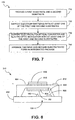
- FIG. 7 A representative method for forming an integrated package of the invention is depicted in the flowchart of FIG. 7.
- a first substrate and a second substrate are provided (block 710).
- an electron emitter and associated driving circuitry are supported by at least one of the first and second substrates.
- an electrical-to-optical converter and an electro-optic modulator are supported by at least one of the first and second substrates.
- the first substrate and second substrate are arranged to form an integrated package. In some embodiments, this can include directly and fixedly attaching the substrates to each other. Attachment of the substrates also can form an hermetically-sealed environment within the integrated package in some embodiments.
- integrated package 310 includes a first substrate 802, which supports electron emitter 150 and associated driving circuitry 808, and a second substrate 804, which includes a electrical-to-optical converter 160, an electro-optic element 810 and associated driving circuitry 812.
- Integrated package 310 also includes at least one diffractive element 820 that optically communicates with the electro-optic element.
- the diffractive element is arranged so that the electro-optic element is at least partially disposed between the electrical-to-optical converter and the diffractive element.
- diffractive element 820 is formed directly onto the electro-optic element; however, various other configurations can be used. Regardless of the particular configuration used, the diffractive element may be constructed to direct and/or focus the modulated light propagated from the electro-optic element. For example, the diffractive element can be used to direct and/or focus the modulated light so that it can be propagated to an optical transmission medium, e.g. , medium 110 of FIG. 1.
- an optical transmission medium e.g. , medium 110 of FIG. 1.
- integrated package 310 of FIG. 8 includes at least one optical filter 824 that optically communicates with the electrical-to-optical converter.
- an optical filter allows one or more selected frequencies of the light generated by the electrical-to-optical converter to be emitted from the integrated package.
- one or more of the diffractive element and the optical filter can be arranged within cavity 823.
- the substrates 802 and 804 form a enclosure that encases at least the optical source.
- a robust modulated light source can be produced.
- the enclosure can protect one or more of the components from damage, such as may occur during component handling.
- the integrated package forms a hermetic seal about at least some of the components, the potential for degradation of device performance due to contamination of those components, for example, can be reduced.
- the hermetic seal also enables the cavity to be evacuated.
- the exemplary technique depicted in FIG. 9 includes providing two substrates (902, 904) that are substantially planar.
- the various components can be supported by, e.g., formed on and/or in, the substrates and then the substrates can be arranged in a substantially fixed spacial relationship relative to each other. In the embodiment depicted in FIG. 9, this is accomplished by arranging mounting components (906, 908) between the substrates. In this manner, a cavity is formed between the substrates by the mounting components maintaining the substrates in a spaced relationship from each other.
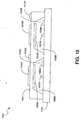
- Arrays capable of producing multiple modulated light beams also can be formed.
- an embodiment of an integrated package that incorporates an array of optical sources is depicted in FIG. 10.
- Integrated package 1000 of FIG. 10 includes a lower substrate 1002 and an upper substrate 1004.
- Substrate 1002 engages upper substrate 1004 to define multiple cavities (1005A, 1005B).
- the upper substrate includes recesses (1006A, 1006B), each of which defines a cavity.
- Substrate 1002 supports multiple electron emitters (1007A, 1007B) and associated driving circuitry (1008A, 1008B).
- Substrate 1004 supports electrical-to-optical converters (1009A, 1009B), electro-optic elements (1010A, 1010B) and associated driving circuitry (1012A, 1012B). More specifically, an electron emitter and its associated driving circuitry, and an electrical-to-optical converter are arranged within each cavity.
- each upper substrate could define one recess that defines a cavity for receiving an optical source.
- Each optical source of an integrated package need not exhibit the same optical properties, e.g. , wavelength, as another. Therefore, the array of optical sources of such an integrated package may be used in a Wavelength Division Multiplexing (WDM) application.
- WDM Wavelength Division Multiplexing
- multiple individual light signals are modulated with respect to a carrier wavelength, propagated along the same optical transmission medium, and then deconvolved at a receiving end.
Landscapes
- Physics & Mathematics (AREA)
- Nonlinear Science (AREA)
- General Physics & Mathematics (AREA)
- Optics & Photonics (AREA)
- Optical Modulation, Optical Deflection, Nonlinear Optics, Optical Demodulation, Optical Logic Elements (AREA)
- Common Detailed Techniques For Electron Tubes Or Discharge Tubes (AREA)
Applications Claiming Priority (2)
| Application Number | Priority Date | Filing Date | Title |
|---|---|---|---|
| US10/104,099 US6590692B1 (en) | 2002-03-22 | 2002-03-22 | Producing modulated light using electron emitters |
| US104099 | 2002-03-22 |
Publications (3)
| Publication Number | Publication Date |
|---|---|
| EP1347547A2 EP1347547A2 (en) | 2003-09-24 |
| EP1347547A3 EP1347547A3 (en) | 2005-06-01 |
| EP1347547B1 true EP1347547B1 (en) | 2007-09-26 |
Family
ID=22298668
Family Applications (1)
| Application Number | Title | Priority Date | Filing Date |
|---|---|---|---|
| EP02024735A Expired - Lifetime EP1347547B1 (en) | 2002-03-22 | 2002-11-06 | Producing modulated light using electron emitters |
Country Status (4)
| Country | Link |
|---|---|
| US (1) | US6590692B1 (enExample) |
| EP (1) | EP1347547B1 (enExample) |
| JP (1) | JP2003287726A (enExample) |
| DE (1) | DE60222625T2 (enExample) |
Family Cites Families (8)
| Publication number | Priority date | Publication date | Assignee | Title |
|---|---|---|---|---|
| US4800263A (en) * | 1987-02-17 | 1989-01-24 | Optron Systems, Inc. | Completely cross-talk free high spatial resolution 2D bistable light modulation |
| GB2271464A (en) * | 1992-08-21 | 1994-04-13 | Sharp Kk | Photoemission apparatus. |
| JPH06260113A (ja) * | 1993-03-05 | 1994-09-16 | Mitsubishi Electric Corp | 陰極線管 |
| JP2944877B2 (ja) * | 1993-12-27 | 1999-09-06 | ミヨタ株式会社 | 光書き込み用小型陰極線管 |
| US6292598B1 (en) * | 1998-11-04 | 2001-09-18 | Corvis Corporation | Optical transmission apparatuses, methods, and systems |
| US6414781B1 (en) * | 1999-03-30 | 2002-07-02 | Seiko Epson Corporation | Electro-optical device and projection display device including the same |
| JP2001209017A (ja) * | 1999-11-15 | 2001-08-03 | Mitsubishi Electric Corp | 光電変換半導体装置 |
| JP2002040503A (ja) * | 2000-07-26 | 2002-02-06 | Taiyo Yuden Co Ltd | 波長変換装置 |
-
2002
- 2002-03-22 US US10/104,099 patent/US6590692B1/en not_active Expired - Fee Related
- 2002-11-06 DE DE60222625T patent/DE60222625T2/de not_active Expired - Lifetime
- 2002-11-06 EP EP02024735A patent/EP1347547B1/en not_active Expired - Lifetime
-
2003
- 2003-03-18 JP JP2003074063A patent/JP2003287726A/ja not_active Withdrawn
Non-Patent Citations (1)
| Title |
|---|
| None * |
Also Published As
| Publication number | Publication date |
|---|---|
| US6590692B1 (en) | 2003-07-08 |
| EP1347547A3 (en) | 2005-06-01 |
| JP2003287726A (ja) | 2003-10-10 |
| DE60222625D1 (de) | 2007-11-08 |
| EP1347547A2 (en) | 2003-09-24 |
| DE60222625T2 (de) | 2008-07-10 |
Similar Documents
| Publication | Publication Date | Title |
|---|---|---|
| US7501747B2 (en) | Integrated circuit optical signal emitters | |
| CN112114446B (zh) | 硅光调制器、光发射装置及光信号的调制方法 | |
| US7275877B2 (en) | Optical module having individual housing for an optical processing unit and an optical sub-assembly | |
| EP0430231A2 (en) | Method of optical transmission and optical transmitter used in the same | |
| US11764543B2 (en) | Integration of modulator and laser in a single chip | |
| CN115702529B (zh) | 光电模块、用于操作光电模块的方法及头戴式显示器 | |
| EP0987802A2 (en) | Optical communication module | |
| EP3557706B1 (en) | Communication system employing surface-coupled optical devices | |
| US5764400A (en) | Optical modulator | |
| US20060126684A1 (en) | Real time constant excitation ratio (ER) laser driving circuit | |
| US11539444B2 (en) | Phase modulator for optical signal using multimode interference couplers | |
| JP2009146992A (ja) | 光モジュール | |
| EP1347547B1 (en) | Producing modulated light using electron emitters | |
| CN110959233B (zh) | 包括移相器的光信号发生器 | |
| US6894273B2 (en) | Systems and methods for producing modulated light beams | |
| US20240069367A1 (en) | Optical module | |
| EP1017141A2 (en) | Modulator-integrated laser module | |
| EP1043817A2 (en) | Light emitting module | |
| JP2860666B2 (ja) | 光機能素子 | |
| GB2278716A (en) | Optical fibre laser incorporating polymeric waveguide | |
| JP5918787B2 (ja) | 波長多重送信器 | |
| JPS6017717A (ja) | 半導体光変調素子 | |
| JPH0213911A (ja) | 光デバイス | |
| JP2005217401A (ja) | レーザダイオードシステム、レーザダイオードの配列方法及びレーザダイオードの光学的配列 | |
| CN118050918A (zh) | 光学集成电路模块和光学通信设备 |
Legal Events
| Date | Code | Title | Description |
|---|---|---|---|
| PUAI | Public reference made under article 153(3) epc to a published international application that has entered the european phase |
Free format text: ORIGINAL CODE: 0009012 |
|
| AK | Designated contracting states |
Kind code of ref document: A2 Designated state(s): AT BE BG CH CY CZ DE DK EE ES FI FR GB GR IE IT LI LU MC NL PT SE SK TR |
|
| AX | Request for extension of the european patent |
Extension state: AL LT LV MK RO SI |
|
| PUAL | Search report despatched |
Free format text: ORIGINAL CODE: 0009013 |
|
| AK | Designated contracting states |
Kind code of ref document: A3 Designated state(s): AT BE BG CH CY CZ DE DK EE ES FI FR GB GR IE IT LI LU MC NL PT SE SK TR |
|
| AX | Request for extension of the european patent |
Extension state: AL LT LV MK RO SI |
|
| RIC1 | Information provided on ipc code assigned before grant |
Ipc: 7G 02F 1/00 B Ipc: 7H 01J 1/304 A |
|
| 17P | Request for examination filed |
Effective date: 20051104 |
|
| AKX | Designation fees paid |
Designated state(s): DE FR GB |
|
| 17Q | First examination report despatched |
Effective date: 20051228 |
|
| RAP1 | Party data changed (applicant data changed or rights of an application transferred) |
Owner name: AVAGO TECHNOLOGIES FIBER IP (SINGAPORE) PTE. LTD. |
|
| GRAP | Despatch of communication of intention to grant a patent |
Free format text: ORIGINAL CODE: EPIDOSNIGR1 |
|
| GRAS | Grant fee paid |
Free format text: ORIGINAL CODE: EPIDOSNIGR3 |
|
| GRAA | (expected) grant |
Free format text: ORIGINAL CODE: 0009210 |
|
| AK | Designated contracting states |
Kind code of ref document: B1 Designated state(s): DE FR GB |
|
| REG | Reference to a national code |
Ref country code: GB Ref legal event code: FG4D |
|
| REF | Corresponds to: |
Ref document number: 60222625 Country of ref document: DE Date of ref document: 20071108 Kind code of ref document: P |
|
| EN | Fr: translation not filed | ||
| PLBE | No opposition filed within time limit |
Free format text: ORIGINAL CODE: 0009261 |
|
| STAA | Information on the status of an ep patent application or granted ep patent |
Free format text: STATUS: NO OPPOSITION FILED WITHIN TIME LIMIT |
|
| 26N | No opposition filed |
Effective date: 20080627 |
|
| PG25 | Lapsed in a contracting state [announced via postgrant information from national office to epo] |
Ref country code: FR Free format text: LAPSE BECAUSE OF FAILURE TO SUBMIT A TRANSLATION OF THE DESCRIPTION OR TO PAY THE FEE WITHIN THE PRESCRIBED TIME-LIMIT Effective date: 20080704 |
|
| PGFP | Annual fee paid to national office [announced via postgrant information from national office to epo] |
Ref country code: DE Payment date: 20121031 Year of fee payment: 11 |
|
| PGFP | Annual fee paid to national office [announced via postgrant information from national office to epo] |
Ref country code: GB Payment date: 20121031 Year of fee payment: 11 |
|
| REG | Reference to a national code |
Ref country code: DE Ref legal event code: R082 Ref document number: 60222625 Country of ref document: DE Representative=s name: DILG HAEUSLER SCHINDELMANN PATENTANWALTSGESELL, DE |
|
| REG | Reference to a national code |
Ref country code: GB Ref legal event code: 732E Free format text: REGISTERED BETWEEN 20130725 AND 20130731 |
|
| REG | Reference to a national code |
Ref country code: DE Ref legal event code: R081 Ref document number: 60222625 Country of ref document: DE Owner name: AVAGO TECHNOLOGIES GENERAL IP (SINGAPORE) PTE., SG Free format text: FORMER OWNER: AVAGO TECHNOLOGIES FIBER IP (SINGAPORE) PTE. LTD., SINGAPORE, SG Effective date: 20130723 Ref country code: DE Ref legal event code: R082 Ref document number: 60222625 Country of ref document: DE Representative=s name: DILG HAEUSLER SCHINDELMANN PATENTANWALTSGESELL, DE Effective date: 20130723 |
|
| GBPC | Gb: european patent ceased through non-payment of renewal fee |
Effective date: 20131106 |
|
| PG25 | Lapsed in a contracting state [announced via postgrant information from national office to epo] |
Ref country code: DE Free format text: LAPSE BECAUSE OF NON-PAYMENT OF DUE FEES Effective date: 20140603 |
|
| REG | Reference to a national code |
Ref country code: DE Ref legal event code: R119 Ref document number: 60222625 Country of ref document: DE Effective date: 20140603 |
|
| PG25 | Lapsed in a contracting state [announced via postgrant information from national office to epo] |
Ref country code: GB Free format text: LAPSE BECAUSE OF NON-PAYMENT OF DUE FEES Effective date: 20131106 |