BACKGROUND OF THE INVENTION
FIELD OF THE INVENTION
The invention relates to a method of manufacturing
surface-discharge-scheme alternating-current-type plasma display
panels, and more particularly, to a method of forming components,
such as a dielectric layer and the like, of the plasma display panel.
The present application claims priority from Japanese
Application No. 2002-68149, the disclosures of which are
incorporated herein by reference for all purposes.
DESCRIPTION OF THE RELATED ART
At the present time, surface-discharge-type AC plasma display
panels (hereinafter referred to as "PDP") have received attention
as large-sized flat color-screen displays, and have increasingly
become commonly used in ordinary homes.
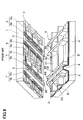
Figs. 6 and 7 illustrate the configuration of a
surface-discharge-type alternating-current PDP which has been
proposed by the present applicant. Fig. 6 is a schematically
perspective view of the proposed PDP when the front glass substrate
is disassembled from the back glass substrate . Fig. 7 is a sectional
view taken along the column direction of the PDP at a central point
in discharge cells.
The PDP in Figs. 6 and 7 includes a front glass substrate 1
having a back surface on which a plurality of row electrode pairs
(X, Y) are arranged at regular intervals in the column direction
and each extends in the row direction. Each of the row electrodes
X and Y forming the row electrode pair (X, Y) is constructed of
T-shaped transparent electrodes Xa (Ya) and a bus electrode Xb (Yb)
extending in the row direction. The transparent electrodes Xa and
Ya are opposite to each other with a discharge gap g set at a required
distance and interposed in between.
A dielectric layer 2 is also formed on the back surface of
the front glass substrate 1 so as to cover the row electrode pairs
(X, Y) . In turn, additional dielectric layers 3 are formed on the
back surface of the dielectric layer 2, and covered with a protective
layer (not shown) made of MgO.
Further, a black additional layer 3A formed of a black
light-absorbing material is formed on a portion of the additional
dielectric layer 3 and opposite a zone between the bus electrodes
Xb (Yb) of the back-to-back row electrodes X (Y).
On a surface of a back glass substrate 4 on the display screen
side, a plurality of column electrodes D and a column electrode
protective layer 5 covering the column electrodes D are formed,
and then a partition wall 6 is formed on the column electrode
protective layer 5.
The partition wall 6 is constructed of pairs of first transverse
walls 6A, pairs of second transverse walls 6B and transverse walls
6C. The pairs of first transverse walls 6A and the pairs of second
transverse walls 6B are arranged in alternate positions in the column
direction. The first or second transverse walls 6A or 6B in each
pair are positioned back to back in between adjacent display lines.
A clearance r is formed between the second transverse wall
6B and the protective layer covering the additional dielectric layer
3.
The opposing first transverse walls 6A, the opposing second
transverse walls 6B and the vertical walls 6C of the partition wall
6 partition the discharge space defined between the front glass
substrate 1 and the back glass substrate 4 into display discharge
cells C1. Red-, green-, and blue-colored phosphor layers 7 are
each formed in the display discharge cell C1 and are arranged in
order in the row direction.
Further, a protrusion rib 8 protrudes into a space formed
between the two back-to-back second transverse walls 6B and raises
a part of the column electrode D, located between the two second
transverse walls 6B, and the column electrode protective layer 5
covering this column electrode D, to cause them to be in contact
with the black additional layer 3A.
Thus, two addressing discharge cells C2 are formed on both
sides of the protrusion rib 8, and each communicates with the
corresponding display discharge cells C1 through the clearances
r.
When additional layers of a dielectric layer are formed in
multilayer formation as in the case of the above PDP, a lamination
of the additional layers (for example, the additional dielectric
layer 3 and the black additional layer 3A) on the dielectric layer
is carried out by prior art methods typically including the following
steps.
A prior art method using a photosensitive dielectric film for
forming the lamination of the additional layers of the dielectric
layer is here described.
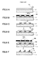
Initially, as illustrated in Fig. 8A, a photosensitive
dielectric film F1 is laminated on the dielectric layer 2 of the
glass substrate 1 on which the row electrodes (not shown) and the
dielectric layer 2 are formed. Then, as illustrated in Fig. 8B,
a mask M1 having through-holes M1a formed therein in correspondence
with positions and shape of additional dielectric layers 3 to be
formed is laid on the photosensitive dielectric film F1. The
photosensitive dielectric film F1 is exposed to light through the
mask M1 to undergo patterning.
Then, as illustrated in Fig. 8C, the photosensitive dielectric
film F1 is developed to remove the unexposed regions, and then the
remaining exposed regions are burned to form additional dielectric
layers 3.
Then, as illustrated in Fig. 8D, a photosensitive dielectric
film F2 is laminated on the dielectric layer 2 and the additional
dielectric layers 3 which is formed as described.
Then, similarly, as illustrated in Fig. 8E, a mask M2 having
through-holes M2a formed therein in correspondence with positions
and shape of additional dielectric layers 3A to be formed is laid
on the photosensitive dielectric film F2. The photosensitive
dielectric film F2 is exposed to light through the mask M2 to undergo
patterning.
After this patterning process, as illustrated in Fig. 8F, the
photosensitive dielectric film F2 is developed to remove the
unexposed regions, and then the remaining exposed regions are burned
to form additional dielectric layers 3A.
However, in the case of the above prior art method using a
photosensitive dielectric layer for forming the additional layers
of the dielectric layer in multilayer form, when the photosensitive
dielectric film F2 is laminated in order to form the additional
dielectric layers 3A which is the second layer, protrusions and
hollows presented by the pre-formed additional dielectric layers
3 cause crinkles in the photosensitive dielectric film F2, and
therefore adhesion between the photosensitive dielectric film F2
and the dielectric layer 2 is insufficient, giving rise to a problem
of peeling in the developing or burning process.
Further, with this prior art method, the initially formed
additional dielectric layers 3 are shrunk in shape in the burning
process. This shrinkage results in the strict necessity for high
precision in alignment in the patterning process for the second
layer for the additional dielectric layers 3A. The uneven top
surfaces of the additional dielectric layers 3 after undergoing
the burning process gives rise to a problem of the sliding of the
photosensitive dielectric film F2 during the developing process
for forming the second layer for the additional dielectric layers
3A.
The prior art method has further problems of an increase in
manufacturing costs and a decrease in efficiency of working because
of the increase in manufacturing steps due to repeating the exposure,
development and burning processes for forming the first layer and
the second layer which are to be the additional layers of the
dielectric layer.
The prior art method has yet another problem of a relatively
positional deviation produced between the pattern of the row
electrode and the additional layers of the dielectric layer because
the repeating of the burning processes creates deformation or
shrinkage of the glass substrate 1.
Another prior art method using pattern printing for multilayer
formation of additional layers of the dielectric layer is now
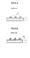
described. First, as illustrated in Fig. 9A, a low-melting glass
paste 3' is pattern-printed and dried onto a predetermined position
on the dielectric layer 2 of the glass substrate 1 on which the
row electrodes (not shown) and the dielectric layer 2 are formed,
so as to be shaped in correspondence with the shape of the additional
dielectric layer to be formed.
In addition, as illustrated in Fig. 9B, another low-melting
glass paste 3A' is pattern-printed and dried onto a predetermined
position on the pattern-printed and dried low-melting glass paste
3' so as to be shaped in correspondence with the shape of the
additional dielectric layer to be formed.
After that, the low-melting glass pastes 3' and 3A' formed
in double-layer formation are burned to form two laminated
additional dielectric layers.
However, the above prior art method using pattern printing
also has problems of the difficulty in alignment between the
additional layers of the dielectric layer in maultilayer formation
because of the low precision of pattern printing, and also of the
likelihood of low precision in the multilayer dimensions of the
formed additional dielectric layers because of wide variations in
film-thickness of the low-melting glass paste 3' and 3A' formed
by pattern printing.
SUMMARY OF THE INVENTION
The present invention has been made to solve the various
problems arising in the prior art processes of multilayer lamination
of additional layers of a dielectric layer in plasma display panels
as described above.
It is therefore an object of the present invention to provide
a method of manufacturing plasma display panels capable of forming
and laminating dielectric layers in multilayer formation with a
reduced number of processes and also providing a high precision.
To attain the above object, a manufacturing method of plasma
display panels according to the present invention relates to a
manufacturing method for forming lamination of a plurality of
dielectric layers on a substrate of the plasma display panel, having
a first feature of including the steps of: a forming process for
forming a photosensitive glass material layer forming the dielectric
layers; a patterning process for exposing required parts of the
photosensitive glass material layer, formed by the forming process,
to light; repeating the forming process and the patterning process
for each of the photosensitive glass material layers to be formed
and laminated on the substrate; a developing process for
concurrently removing unexposed parts from all of the formed and
laminated photosensitive glass material layers after completion
of the forming process and the patterning process for each
photosensitive glass material layer; and a burning process for
concurrently burning all of the formed and laminated photosensitive
glass material layers having been subjected to the developing
process.
With the manufacturing method for plasma display panels
according to the first feature, for example, when additional layers
of a dielectric layer covering discharge electrodes formed on a
substrate of the plasma display panel are laminated in multilayer
form on the dielectric layer in order to limit the spreading of
a discharge, the forming process for a photosensitive glass material
layer, and the patterning process for exposing to light the
photosensitive glass material layer, formed in the forming process,
to pattern it with dielectric layers of a required shape at required
positions are repeatedly performed on each of the photosensitive
glass material layers for multilayer formation of the dielectric
layers to be laminated.
After all of the required photosensitive glass material layers
have been formed, and the patterning performed thereon, the
laminated photosensitive glass material layers all undergo at the
same time the developing process for removing the parts of the
photosensitive glass material layer unexposed in the patterning
process so that the remaining exposed parts will form dielectric
layers such as the additional layers having the required shape,
and undergo the burning process for solidifying the photosensitive
glass material layers provided by the developing process.
As described above, according to the first feature, the
developing process is performed concurrently on all of the
photosensitive glass material layers after completion of the forming
process for each of the multilayered photosensitive glass material
layers. Hence, each of the second and later photosensitive glass
material layers is formed on a photosensitive glass material layer
that has not experienced the developing process. The resulting
flat formation of the top surface of the photosensitive glass
material layer leads to a significant increase in the positional
precision between the dielectric layers to be laminated in
multilayer form, as compared with the prior art manufacturing
methods.
The burning process is finally performed concurrently on the
photosensitive glass material layers. The photosensitive glass
material layers are not burned repeatedly as was done in prior art
methods, to prevent an inferior precision in alignment and the
occurrence of positional deviation between the electrodes formed
on the substrate and the dielectric layers laminated in multilayer
form.
Further, the developing process and the burning process are
each performed only one time, leading to simplification of the
manufacturing process of the plasma display panel, and naturally
reduction in the manufacturing cost.
To attain the aforementioned object, the manufacturing method
for plasma display panels has, in addition to the configuration
of the first feature, a second feature that the photosensitive glass
material layer is formed of glass materials having lead oxide and
silicon dioxide as their main components, and glass materials
including photosensitive resin made from an acrylic-type monomer
or oligomer.
To attain the aforementioned object, the manufacturing method
for plasma display panels has, in addition to the configuration
of the first feature, a third feature that the photosensitive glass
material layer is burned at temperatures in the vicinity of a
softening point of the glass materials forming the photosensitive
glass material layer.
To attain the aforementioned object, the manufacturing method
for plasma display panels has, in addition to the configuration
of the third feature, a fourth feature that the burning temperature
ranges from 560 degrees C. to 580 degrees C.
To attain the aforementioned object, the manufacturing method
for plasma display panels has, in addition to the configuration
of the first feature, a fifth feature that a non-photosensitive
glass material layer is formed on the substrate prior to the forming
of the initial layer of the photosensitive glass material layers,
and undergoes the burning process concurrently with the laminated
photosensitive glass material layers.
With the manufacturing method for plasma display panels
according to the fifth feature, the non-photosensitive glass
material layer forming the dielectric layer covering the electrodes
formed on the substrate, is formed on the substrate prior to the
forming of the photosensitive glass material layers to be laminated
in multilayer form. Then the burning process for the
non-photosensitive glass material layer is performed concurrently
with the burning process for the laminated photosensitive glass
material layers.
Therefore, positional deviation between the dielectric layers
after their formation is prevented and simplification of the
manufacturingprocess to reduce the manufacturing costs is provided.
To attain the aforementioned object, the manufacturing method
for plasma display panels has, in addition to the configuration
of the fifth feature, a sixth feature that the non-photosensitive
glass material layer is formed of glass materials having lead oxide
and silicon dioxide having softening point temperatures of about
560 degrees C. as their main components, and glass materials
including non-photosensitive resin made from an acrylic-type
polymer.
To attain the aforementioned object, the manufacturing method
for plasma display panels has, in addition to the configuration
of the fifth feature, a seventh feature that the non-photosensitive
glass material layer and the photosensitive glass material layer
are formed of the glass materials approximately equal to each other
in softening point temperatures.
With the manufacturing method for plasma display panels
according to the seventh feature, the use of glass materials roughly
equal in softening point temperature to form the non-photosensitive
and photosensitive glass material layers allows the burning process
to be performed concurrently on the non-photosensitive and
photosensitive glass material layers.
To attain the aforementioned object, the manufacturing method
for plasma display panels has, in addition to the configuration
of the fifth feature, an eighth feature that the dielectric layer
provided by the photosensitive glass material layer is an additional
layer of the dielectric layer provided by the non-photosensitive
glass material layer.
With the manufacturing method of plasma display panels
according to the eighth feature, at required positions on the
dielectric layer provided by the non-photosensitive glass material
layer, the photosensitive glass material layer forms the additional
layers of required dimensions allowing for limitation of the
spreading of a discharge in the discharge space, or the like.
To attain the aforementioned object, the manufacturing method
for plasma display panel has, in addition to the configuration of
the first feature, a ninth feature that the formation of the
photosensitive glass material layer on the substrate in the forming
process is carried out by pre-coating of a glass paste on a supporting
film and then bonding of the resulting photosensitive glass material
layer onto the substrate by pressure.
With the manufacturing method for plasma display panels
according to the ninth feature, in order to form the photosensitive
glass material layer on the substrate, a glass paste is not coated
directly on the substrate, and alternatively the glass paste is
previously coated on the supporting film and dried thereon to prepare
a film having a photosensitive glass layer with a required thickness
formed thereon. The film-form photosensitive glass material layer
is bonded by pressure while the supplying film is being peeled from
it, to form a photosensitive glass material layer on the substrate.
As a result, the manufacturing process of the plasma display
panels is simplified and the photosensitive glass material layer
has an advantage of being formed to a desired and uniform thickness
on the substrate.
To attain the aforementioned object, the manufacturing method
for plasma display panels has, in addition to the configuration
of the ninth feature, a tenth feature that while the supporting
film is peeled from the photosensitive glass material layer formed
on the supporting film, the photosensitive glass material layer
is bonded on the substrate by pressure in a heated state by use
of a roller.
To attain the aforementioned object, the manufacturing method
for plasma display panels has, in addition to the configuration
of the first feature, an eleventh feature that in the patterning
process, each of the photosensitive glass material layers is exposed
to light through a mask having through-holes corresponding to
positions and shape of the dielectric layers provided by the
photosensitive glass material layer.
With the manufacturing method for plasma display panels
according to the eleventh feature, for each of the dielectric layers
to be laminated in multilayer form, a mask having the through-holes
corresponding to the positions and shape of the individual
dielectric layer can be prepared in advance or alternatively can
be formed on the corresponding photosensitive glass material layer.
Each photosensitive glass material layer is exposed to light through
the corresponding mask in the patterning process in order to be
readily laminated as a dielectric layer of a desired shape in a
desired position.
These and other objects and features of the present invention
will become more apparent from the following detailed description
with reference to the accompanying drawings.
BRIEF DESCRIPTION OF THE DRAWINGS
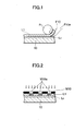
Fig. 1 is a diagram illustrating a forming process for a
photosensitive glass material layer in accordance with the present
invention.
Fig. 2 is a diagram illustrating a patterning process.
Fig. 3 is a diagram illustrating a forming process when another
photosensitive glass material layer is formed for lamination.
Fig. 4 is a diagram illustrating a patterning process for the
photosensitive glass material layer formed and laminated.
Fig. 5 is a diagram illustrating a developing process and a
burning process.
Fig. 6 is a perspective view illustrating an example of plasma
displaypanels having dielectric layers formed therein inmultilayer
form.
Fig. 7 is a vertically sectional view of the plasma display
panel in Fig. 6.
Fig. 8A is a diagram illustrating a first process in an example
of prior art manufacturing methods for plasma display panels.
Fig. 8B is a diagram illustrating a second process in the example
of the prior art manufacturing methods.
Fig. 8C is a diagram illustrating a third process in the example
of the prior art manufacturing methods.
Fig. 8D is a diagram illustrating a fourth process in the example
of the prior art manufacturing methods.
Fig. 8E is a diagram illustrating a fifth process in the example
of the prior art manufacturing methods.
Fig. 8F is a diagram illustrating a sixth process in the example
of the prior art manufacturing methods.
Fig. 9A is a diagram illustrating a first process in another
example of prior art manufacturing methods for plasma display
panels.
Fig. 9B is a diagram illustrating a second process in the
alternative example of the prior art manufacturing methods.
DETAILED DESCRIPTION OF THE PREFERRED EMBODIMENT
One of prefer red embodiments according to the present invention
will be described hereinafter in detail with reference to the
accompanying drawings.
Fig. 1 to Fig. 5 are diagrams illustrating a manufacturing
method for plasma display panels (hereinafter referred to as "PDP")
in an embodiment according to the present invention.
In the manufacturing method for PDP in the embodiment, first,
row electrodes (not shown) and a non-photosensitive glass material
layer L0 are formed on a glass substrate 10.
If the glass substrate 10 is a front glass substrate situated
on the display screen side of the PDP, the row electrodes are formed
such that a transparent conductive film made of ITO or the like
is evaporated onto the glass substrate 10, and then is patterned
with a letter-T shape by using photolithography techniques. Next,
a photosensitive silver paste is so coated as to be connected with
base ends of the T-shaped transparent conductive films, then is
dried, and then is patterned with a band shape by use of
photolithography techniques.
The non-photosensitive glass material layer L0 is formed of
non-photosensitive glass materials, and in such a manner that a
low-melting glass paste including glass materials having lead oxide
and silicon dioxide of softening-point temperatures of about 560
degrees C. as their main components, and non-photosensitive resin
made from an acrylic-type polymer, is coated on the surface of the
glass substrate 10 having the row electrodes formed thereon, and
then dried.
Next, as illustrated in Fig. 1, while a base film F10a is being
peeled from a photosensitive resin film F10, the photosensitive
resin film F10 is bonded onto the non-photosensitive glass material
layer L0, formed on the glass substrate 10, in a heated state by
use of a roller R to form a first photosensitive glass material
layer L1.
To fabricate the photosensitive resin film F10 forming the
first photosensitive glass material layer L1, a low-melting glass
paste including glass materials having lead oxide and silicon
dioxide as their main components, and photosensitive resin made
from an acrylic-type monomer or oligomer, and having a softening
point temperature roughly equal to that of the glass materials for
forming the non-sensitive glass material layer L0, is coated on
the base film F10a and then dried.
Next, as illustrated in Fig. 2, the first photosensitive glass
material layer L1 formed on the glass substrate 10 is exposed to
light through a resist mask M10 having through-holes M10a of a
required shape formed therein in required positions, to be
patterned.
To form the resist mask M10, a film-form resist is laminated
on the first photosensitive glass material layer L1, and then the
resists is exposed to light and developed by use of a mask having
a predetermined pattern in order that the through-holes M10a are
opened in positions of the resist corresponding to where first
additional layers of the dielectric layer are to be formed, and
each has a shape identical with the outline of the first additional
layer.
In this manner, following the completion of the patterning
process for the first photosensitive glass material layer L1, the
resist mask M10 is peeled from the first photosensitive glass
material layer L1.
As illustrated in Fig. 3, then, as in the case of the
photosensitive resin film F10, while a base film F11a is being peeled
from a photosensitive resin film F11, the photosensitive resin film
F11 is bonded on the first photosensitive glass material layer L1,
undergone the patterning process, in a heated state by the use of
roller R to form a second photosensitive glass material layer L2.
To make the photosensitive resin film F11, a low-melting glass
paste having approximately the same softening point temperature
and approximately the same components as those of the photosensitive
resin film F10 used for forming the first photosensitive glass
material layer L1 is coated on the base film F11a and dried.
Then, as illustrated in Fig. 4, as in the case of the formation
of the first photosensitive glass material layer L1, the second
photosensitive glass material layer L2 is exposed to light through
a resist mask M11 formed on the second photosensitive glass material
layer L2 and having through-holes M11a opened in positions therein
corresponding to positions where second additional layers of the
dielectric layer are to be formed, and each having a shape identical
with the outline of the second additional layer, to be patterned.
Following the completion of the patterning process for the
second photosensitive glass material layer L2, the resist mask M11
is peeled from the second photosensitive glass material layer L2.
Then, as illustrated in Fig. 5, the first photosensitive glass
material layer L1 and the second photosensitive glass material layer
L2 each undergone the patterning process as described above are
developed at the same time.
Then, the first photosensitive glass material layer L1, the
second photosensitive glass material layer L2, and the
non-photosensitive glass material layer L0 all of which undergone
the developing process are concurrently burned at a temperature
(e.g. from about 560 to 580 degrees C.) in the vicinity of their
softening points. Hence, the non-photosensitive glass material
layer L0 forms a dielectric layer 11, the first photosensitive glass
material layer L1 forms a first additional dielectric layer 12,
and the second photosensitive glass material layer L2 forms a second
additional dielectric layer 13.
As described above, with the foregoing manufacturing method,
after the patterning process for and before the developing process
for the first photosensitive glass material layer L1, the forming
process and the patterning process are performed on the second
photosensitive glass material layer L2. After that, the developing
process is performed concurrently on the first photosensitive glass
material layer L1 and the second photosensitive glass material layer
L2. Because of these steps, the first photosensitive glass material
layer L1 has a flat surface when the second photosensitive glass
material layer L2 is formed thereon. For this reason, a
significantly high positional precision between the additional
dielectric layer 12 and the additional dielectric layer 13 which
are to be formed is provided as compared with that in prior art
manufacturing methods.
Further, all of the non-photosensitive glass material layer
L0 and the first and second photosensitive material layer L1 and
L2 are finally burned at the same time. This prevents an inferior
precision in alignment and the occurrence of positional deviation
among the row electrodes, the additional dielectric layer 12, and
the additional dielectric layer 13, which are produced by repeating
the burning processes as in the prior art manufacturing methods.
Further, the developing process and the burning process are
each performed only one time, leading to simplification of the
manufacturing process to reduce in the manufacturing cost.
In the above-mentioned manufacturing method, to form the
non-photosensitive glass material layer L0, a low-melting glass
paste including glass materials having lead oxide and silicon
dioxide having a softening-point temperature of about 560 degrees
C. as their main components, and non-photosensitive resin made from
an acrylic-type polymer may be coated on a base film and dried.
The resulting non-photosensitive glass material layer may be bonded
on the glass substrate 10 by pressure.
The non-photosensitive glass material layer L0 formed by using
the film-form non-photosensitive glass material layer as described
above may be burned together with the first and second photosensitive
glass material layers L1 and L2.
In the embodiment, each of the first photosensitive glass
material layer L1 and the second photosensitive glass material layer
L2 is patterned by use of the dedicated mask formed of resist film
which is exposed to light for patterning and then developed. However,
each patterning process may use a mask having required through-holes
pre-formed therein.
The first and second photosensitive glass material layers in
the embodiment is a negative type, so that their unexposed regions
are removed by the developing process.
In the embodiment, the formation of the dielectric layer 11
uniformly covering the inner surface of the glass substrate 10 and
the row electrodes is carried out by coating and burning of the
non-photosensitive glass material layer, but the dielectric layer
may be formed of a negative-type photosensitive glass material
layer.
In this case, after the formation of the photosensitive glass
material layer, the full surface of the photosensitive glass
material layer is exposed to light.
Then, the developing process and the burning process for the
photosensitive glass material layer forming the dielectric layer
11 may be respectively performed simultaneously with the developing
process and the burning process for the first and second
photosensitive glass material layers.
Still further, the embodiment describes the manufacturing
method of using a photosensitive resin film to form the first and
second photosensitive glass material layers. However, the
formation of each of the first and second photosensitive glass
material layers may be carried out by coating of a photosensitive
glass paste by use of printing techniques, roll-coating techniques,
or the like.
The terms and description used herein are set forth by way
of illustration only and are not meant as limitations. Those skilled,
in the art will recognize that numerous variations are possible
within the spirit and scope of the invention as defined in the
following claims.