EP1345136A1 - Modellierung einer elektronischen Vorrichtung - Google Patents
Modellierung einer elektronischen Vorrichtung Download PDFInfo
- Publication number
- EP1345136A1 EP1345136A1 EP03000829A EP03000829A EP1345136A1 EP 1345136 A1 EP1345136 A1 EP 1345136A1 EP 03000829 A EP03000829 A EP 03000829A EP 03000829 A EP03000829 A EP 03000829A EP 1345136 A1 EP1345136 A1 EP 1345136A1
- Authority
- EP
- European Patent Office
- Prior art keywords
- electrical behavior
- measured
- modeling
- signal
- response
- Prior art date
- Legal status (The legal status is an assumption and is not a legal conclusion. Google has not performed a legal analysis and makes no representation as to the accuracy of the status listed.)
- Granted
Links
Images



Classifications
-
- G—PHYSICS
- G06—COMPUTING OR CALCULATING; COUNTING
- G06F—ELECTRIC DIGITAL DATA PROCESSING
- G06F30/00—Computer-aided design [CAD]
- G06F30/30—Circuit design
- G06F30/36—Circuit design at the analogue level
- G06F30/367—Design verification, e.g. using simulation, simulation program with integrated circuit emphasis [SPICE], direct methods or relaxation methods
Definitions
- Modeling of electronic devices e.g. for simulation of electronic circuits comprising such devices, as known for example from the SPICE circuit simulation system, requires to know or reveal details about the internal construction of the device to be modeled. Often manufacturers of devices (like operational amplifiers) provide model parameter to be used in the SPICE system.
- the measured electrical behavior comprises a measured signal response on a predetermined electrical signal input to the device, and preferably comprises a measured signal response on a step signal.
- the device can contain any kind of element like - for example - cables, board traces, connectors, packages, sockets, stubs, resistors, inductors or capacitors. Even multiple reflections or frequency dependent parameters like skin effect or dielectric losses can be characterized according to preferred embodiments.
- the corresponding high-speed signal path e.g. between an Automated Test Equipment (ATE) and a Device Under Test (DUT) becomes relevant influence on the measured signals.
- ATE Automated Test Equipment
- DUT Device Under Test
- the device to be modeled is such high-speed signal path, which might be connected between the ATE and the DUT.
- the device to be modeled can also be a line drive output of such ATE, an n-port network, etc.
- the device to be modeled can be characterized in the time domain by at least one of its pulse or step response.
- An ideal pulse allows characterizing the device to be modeled in the time domain.
- Such ideal pulse is infinitely short, infinitely high, has a predetermined energy, and is known as Dirac pulse.
- Dirac pulse is often not sufficiently feasible in reality. Therefore, in a preferred embodiment a substantially ideal pulse or the response to a step input signal is used to build the model out of measurement data.
- the step response can be calculated by an inverse Fourier transformation and subsequent integration of the resulting pulse response.
- sr xy (t) stands for the response at port x on a stimulation at port y with an ideal step signal.
- e ly '(t) stands for the first derivative of the incident wave into port x.
- the symbol "*" stands for the convolution.
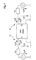
- Fig. 1 shows stimulating incident waves into a 2-port network.
- the relationship between voltages and currents at the ports v1 and v2 of the network are defined by their characteristic impedances Z1 and Z2.
- Fig. 2 shows the SPICE model of the 2-port network of Fig. 1 and Fig. 3 shows the model of a voltage adder.
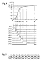
- any arbitrary step response can be approximated with arbitrary accuracy by a section-wise linear curve like in the example shown in the top graph of Fig. 4.
- the corresponding sampling points for the approximation in this example have the time and voltage values listed in Fig. 5.
- the incoming step s(t) is stripped down to the pulses p i (t) having their transitions at the sampling points used for approximation.
- Those pulses are used to control current sources with a trans-conductance representing the slope in the corresponding section of the step response like depicted in Fig. 6.
- the differential input signals on the voltage controlled current sources G i look like the construction pulses p i in Fig.4.
- a circuit is created that has the step response needed for the device to be modeled.
- the model is linear and time invariant, its response to any arbitrary input signal is equal to the response of the signal path to be characterized in the described embodiment.
- Fig. 7 shows how the four step responses of a 2-port network can be measured using a time domain reflection (TDR) oscilloscope.
- the internal TDR source is dedicated to the first channel CH1. It generates a steep edge with a rise time in the order of 40ps. This can be taken as an approximate ideal step scaled with a factor.
- the delay time relative to the internally generated oscilloscope trigger can be observed as the point in time on the scope graph of channel 1 where the edge starts.
- Setup A places a short circuit at the end of cable 1 generating a reflection coefficient of -1.
- Channel 1 of the oscilloscope sees a pulse with a length that equals the round trip delay of cable 1.
- the delay of single trip of cable 1 can be easily determined by placing markers at the 50% points of the pulse edges and taking half of the time distance between the two markers.
- the two channels capture the same signal but on channel 2 (CH2) the combined delay of cable 1 and cable 2 takes effect.
- the delay of cable 2 can be determined by placing markers at the 50% points of the two channels, reading out the time distance and subtracting the delay time of cable 1.
- the Setups A and B can be regarded as a calibration procedure.
- the reflections at the stimulated port can be observed as superposition to the stimulating time domain reflection pulse on channel 1 of the oscilloscope with an additional roundtrip cable 1 delay.
- the transmitted signals can be observed on channel 2 with an additional delay of cable 2.
- the edge of a TDR edge is usually very fast, it certainly is not a perfect step.
- the ideal step response can be calculated from the measured stimulus and response by the method described below.
- the captured waveforms together with a shape of an ideal step starting at the same time as the stimulus have to be converted into a periodic shape by extending the measured date set with the same edge that has been mirrored at the average value of the first and the last sampling point.
- the resulting signals can then be converted into the frequency domain via Fast Fourier Transformation (FFT).
- FFT Fast Fourier Transformation
- the transfer function results from the division from the output signal by the input signal. Multiplication of transfer function and the ideal step in the frequency domain gives the spectrum of the ideal step response that can be converted back into time domain via inverse FFT.
- the voltage error in the transient analysis strongly depends on the integration method and the time steps of the SPICE simulator.
- the time step should be in the same order of magnitude as the delay time of the transmission lines in the step response model.
- the best way to test those parameters is to stimulate the model with a single edge and verify if the final value is close enough to the theoretical end voltage.
- Fig. 2 Differing from the comprehensive model shown in Fig. 2 there are applications where not all step responses are of interest and for such applications the model can be drastically simplified. In many cases only the transmission of a signal from port 1 to port 2 is necessary. This is the case for example for an environment with 50-Ohm terminations at both ends or for signal paths with only small reflections. In such cases, the responses sr11, sr21, and sr22 can be neglected and deleted from the model. The measurement effort and the model complexity are strongly reduced.
- Another example for the device to be modeled is a line driver controlled by a digital input signal. In this case, there is no response at the control input to anything happening at the output. Therefore s12 and s11 are not necessary.
- step responses can be used to characterize n-port networks with n > 2.
- coupled transmission lines for differential signaling would be an application for it.
- the present invention introduces a new method of modeling linear and time invariant devices like signal paths or n-port networks.
- the principle has been derived from basic transmission line and systems theory and is based on step response measurement with a TDR oscilloscope. It has been validated by the means of a SPICE simulation showing the correlation between an arbitrarily chosen signal path model and the corresponding step response model.
Landscapes
- Engineering & Computer Science (AREA)
- Computer Hardware Design (AREA)
- Physics & Mathematics (AREA)
- Theoretical Computer Science (AREA)
- Microelectronics & Electronic Packaging (AREA)
- Evolutionary Computation (AREA)
- Geometry (AREA)
- General Engineering & Computer Science (AREA)
- General Physics & Mathematics (AREA)
- Measurement Of Resistance Or Impedance (AREA)
Priority Applications (3)
| Application Number | Priority Date | Filing Date | Title |
|---|---|---|---|
| DE60318141T DE60318141T2 (de) | 2003-01-15 | 2003-01-15 | Modellierung einer elektronischen Vorrichtung |
| EP03000829A EP1345136B1 (de) | 2003-01-15 | 2003-01-15 | Modellierung einer elektronischen Vorrichtung |
| US10/635,198 US7379856B2 (en) | 2003-01-15 | 2003-08-06 | Modeling an electronic device |
Applications Claiming Priority (1)
| Application Number | Priority Date | Filing Date | Title |
|---|---|---|---|
| EP03000829A EP1345136B1 (de) | 2003-01-15 | 2003-01-15 | Modellierung einer elektronischen Vorrichtung |
Publications (2)
| Publication Number | Publication Date |
|---|---|
| EP1345136A1 true EP1345136A1 (de) | 2003-09-17 |
| EP1345136B1 EP1345136B1 (de) | 2007-12-19 |
Family
ID=27763498
Family Applications (1)
| Application Number | Title | Priority Date | Filing Date |
|---|---|---|---|
| EP03000829A Expired - Lifetime EP1345136B1 (de) | 2003-01-15 | 2003-01-15 | Modellierung einer elektronischen Vorrichtung |
Country Status (3)
| Country | Link |
|---|---|
| US (1) | US7379856B2 (de) |
| EP (1) | EP1345136B1 (de) |
| DE (1) | DE60318141T2 (de) |
Cited By (1)
| Publication number | Priority date | Publication date | Assignee | Title |
|---|---|---|---|---|
| GB2410874A (en) * | 2004-02-06 | 2005-08-10 | Agilent Technologies Inc | Broadband system models |
Families Citing this family (3)
| Publication number | Priority date | Publication date | Assignee | Title |
|---|---|---|---|---|
| US7092981B2 (en) * | 2002-09-27 | 2006-08-15 | Lucent Technologies Inc. | Non-reciprocal network element that produces an input impedance that is a function of the multiplication-division of its load impedances |
| CN101087148B (zh) * | 2006-06-07 | 2011-01-05 | 鸿富锦精密工业(深圳)有限公司 | 高速差分信号模拟分析系统及方法 |
| US8554529B2 (en) * | 2007-11-30 | 2013-10-08 | Texas Instruments Incorporated | Black box model for large signal transient integrated circuit simulation |
Citations (1)
| Publication number | Priority date | Publication date | Assignee | Title |
|---|---|---|---|---|
| EP1128293A2 (de) * | 2000-02-23 | 2001-08-29 | Agilent Technologies Inc. a Delaware Corporation | Modellierung von nichtlinearen Vorrichtungen |
Family Cites Families (19)
| Publication number | Priority date | Publication date | Assignee | Title |
|---|---|---|---|---|
| US3393363A (en) * | 1963-10-07 | 1968-07-16 | Forster Ind Inc | Amplifying means employing pulse width modulation |
| US3431490A (en) * | 1966-01-14 | 1969-03-04 | Ibm | Apparatus for indicating response of a circuit to an applied pulse |
| US4438404A (en) * | 1982-01-04 | 1984-03-20 | Tektronix, Inc. | Signal sampling system |
| EP0448322A3 (en) * | 1990-03-23 | 1992-11-25 | Tektronix, Inc. | Automatic extraction of pulseparametrics from multi-valued functions |
| US5162723A (en) * | 1991-02-11 | 1992-11-10 | Hewlett-Packard Company | Sampling signal analyzer |
| US5349539A (en) * | 1991-10-28 | 1994-09-20 | Zeelan Technology, Inc. | Behavioral model parameter extractor |
| US5793801A (en) * | 1996-07-09 | 1998-08-11 | Telefonaktiebolaget Lm Ericsson | Frequency domain signal reconstruction compensating for phase adjustments to a sampling signal |
| US5886586A (en) * | 1996-09-06 | 1999-03-23 | The Regents Of The University Of California | General constant frequency pulse-width modulators |
| US5799172A (en) * | 1996-09-10 | 1998-08-25 | Motorola, Inc. | Method of simulating an integrated circuit |
| US6490546B1 (en) * | 1999-05-04 | 2002-12-03 | International Business Machines Corporation | Method for obtaining DC convergence for SOI FET models in a circuit simulation program |
| US6970814B1 (en) * | 2000-03-30 | 2005-11-29 | International Business Machines Corporation | Remote IP simulation modeling |
| US6772400B2 (en) * | 2000-04-28 | 2004-08-03 | Northrop Grumman Corporation | Semi-physical modeling of HEMT high frequency small signal equivalent circuit models |
| JP2002054998A (ja) * | 2000-08-10 | 2002-02-20 | Agilent Technol Inc | 光サンプリングシステム |
| WO2002023212A1 (en) * | 2000-09-18 | 2002-03-21 | Agilent Technologies, Inc. | Method and apparatus for linear characterization of multiterminal single-ended or balanced devices |
| US6458611B1 (en) * | 2001-03-07 | 2002-10-01 | Intel Corporation | Integrated circuit device characterization |
| JP4363790B2 (ja) * | 2001-03-15 | 2009-11-11 | 株式会社東芝 | パラメータ抽出プログラムおよび半導体集積回路の製造方法 |
| US6492798B2 (en) * | 2001-04-27 | 2002-12-10 | Logicvision, Inc. | Method and circuit for testing high frequency mixed signal circuits with low frequency signals |
| US6856148B2 (en) * | 2002-03-08 | 2005-02-15 | Hewlett-Packard Development Company, L.P. | Method and program product for evaluating a circuit |
| US20040096021A1 (en) * | 2002-11-14 | 2004-05-20 | Unb Technologies, Inc. | Communications methods for narrow band demodulation |
-
2003
- 2003-01-15 EP EP03000829A patent/EP1345136B1/de not_active Expired - Lifetime
- 2003-01-15 DE DE60318141T patent/DE60318141T2/de not_active Expired - Lifetime
- 2003-08-06 US US10/635,198 patent/US7379856B2/en not_active Expired - Lifetime
Patent Citations (1)
| Publication number | Priority date | Publication date | Assignee | Title |
|---|---|---|---|---|
| EP1128293A2 (de) * | 2000-02-23 | 2001-08-29 | Agilent Technologies Inc. a Delaware Corporation | Modellierung von nichtlinearen Vorrichtungen |
Non-Patent Citations (3)
| Title |
|---|
| COREY S D ET AL: "Automatic netlist extraction for measurement-based characterization of off-chip interconnect", IEEE TRANSACTIONS ON MICROWAVE THEORY AND TECHNIQUES, OCT. 1997, IEEE, USA, vol. 45, no. 10, pt.2, pages 1934 - 1940, XP002240419, ISSN: 0018-9480 * |
| HAYDEN L A ET AL: "Measurement and characterization of high-speed interconnections using time domain network analysis", ISHM '92 PROCEEDINGS. PROCEEDINGS OF THE 1992 INTERNATIONAL SYMPOSIUM ON MICROELECTRONICS (SPIE VOL.1847), SAN FRANCISCO, CA, USA, 19-21 OCT. 1992, 1992, Reston, VA, USA, Int. Soc. Hybrid Microelectron, USA, pages 144 - 149, XP008016760, ISBN: 0-930815-35-1 * |
| NOVELLINO J: "SYSTEM MEASURES AND MODELS INTERCONNECTS", ELECTRONIC DESIGN, PENTON PUBLISHING, CLEVELAND, OH, US, vol. 41, no. 6, 18 March 1993 (1993-03-18), pages 122,124,126, XP000368037, ISSN: 0013-4872 * |
Cited By (2)
| Publication number | Priority date | Publication date | Assignee | Title |
|---|---|---|---|---|
| GB2410874A (en) * | 2004-02-06 | 2005-08-10 | Agilent Technologies Inc | Broadband system models |
| GB2410874B (en) * | 2004-02-06 | 2007-01-31 | Agilent Technologies Inc | Broadband system models |
Also Published As
| Publication number | Publication date |
|---|---|
| DE60318141T2 (de) | 2008-12-04 |
| EP1345136B1 (de) | 2007-12-19 |
| US7379856B2 (en) | 2008-05-27 |
| US20040138866A1 (en) | 2004-07-15 |
| DE60318141D1 (de) | 2008-01-31 |
Similar Documents
| Publication | Publication Date | Title |
|---|---|---|
| EP2378667A2 (de) | Verfahren zur Kompensierung einer Frequenzeigenschaft eines Erzeugers von beliebigen Wellenformen | |
| TWI595242B (zh) | Time-distance measurement with bandwidth correction | |
| Sanaie et al. | A fast method for frequency and time domain simulation of high-speed VLSI interconnects | |
| US6106563A (en) | Method and apparatus for extracting parameters for an electrical structure | |
| Corey et al. | Interconnect characterization using time-domain reflectometry | |
| US20030208734A1 (en) | Time domain measurement systems and methods | |
| Zeng et al. | Modified rational function modeling technique for high speed circuits | |
| TWI631357B (zh) | 利用頻域內校正之時域測量方法 | |
| EP3176591B1 (de) | Messvorrichtung | |
| Fasig et al. | Introduction to non-invasive current estimation (NICE) | |
| CN111191409B (zh) | 芯片内部硅片管脚信号仿真方法及装置 | |
| US7379856B2 (en) | Modeling an electronic device | |
| CN104777370A (zh) | 利用一端口测量的自动固件去除 | |
| Orlov et al. | Contactless modal phenomena based approach to detecting, identifying, and diagnosing of electrical connections | |
| Beyene et al. | An accurate transient analysis of high-speed package interconnects using convolution technique | |
| Corey et al. | Automatic netlist extraction for measurement-based characterization of off-chip interconnect | |
| Belforte | Digital wave simulation of lossy lines for multi-gigabit applications | |
| CN115151827A (zh) | 一种电磁干扰的测量设备及测量方法 | |
| Chernikova et al. | Analytical models for calculating the time response of two-conductor asymmetric transmission lines | |
| Pettanice et al. | Time and Frequency Macromodeling Techniques for Electromagnetic Systems with Propagation Delays | |
| Morales et al. | Analysis of analog sampled s-parameters data using dsp techniques | |
| Rusek | Reflectometers, Time‐Domain | |
| Joshi et al. | Transmission line pulsed waveform shaping with microwave filters | |
| de Magistris et al. | Identification of a Spice Reduced-Order Model for Lossy Interconnects from Terminal Behavior | |
| Corti et al. | Efficient time-domain simulation of lossy multiconductor lines with non-linear loads |
Legal Events
| Date | Code | Title | Description |
|---|---|---|---|
| PUAI | Public reference made under article 153(3) epc to a published international application that has entered the european phase |
Free format text: ORIGINAL CODE: 0009012 |
|
| 17P | Request for examination filed |
Effective date: 20030710 |
|
| AK | Designated contracting states |
Kind code of ref document: A1 Designated state(s): AT BE BG CH CY CZ DE DK EE ES FI FR GB GR HU IE IT LI LU MC NL PT SE SI SK TR |
|
| AX | Request for extension of the european patent |
Extension state: AL LT LV MK RO |
|
| AKX | Designation fees paid |
Designated state(s): DE FR GB |
|
| 17Q | First examination report despatched |
Effective date: 20040604 |
|
| RAP1 | Party data changed (applicant data changed or rights of an application transferred) |
Owner name: AGILENT TECHNOLOGIES, INC. |
|
| 17Q | First examination report despatched |
Effective date: 20040604 |
|
| RAP1 | Party data changed (applicant data changed or rights of an application transferred) |
Owner name: AGILENT TECHNOLOGIES, INC. |
|
| GRAP | Despatch of communication of intention to grant a patent |
Free format text: ORIGINAL CODE: EPIDOSNIGR1 |
|
| GRAS | Grant fee paid |
Free format text: ORIGINAL CODE: EPIDOSNIGR3 |
|
| RAP1 | Party data changed (applicant data changed or rights of an application transferred) |
Owner name: VERIGY (SINGAPORE) PTE. LTD. |
|
| GRAA | (expected) grant |
Free format text: ORIGINAL CODE: 0009210 |
|
| AK | Designated contracting states |
Kind code of ref document: B1 Designated state(s): DE FR GB |
|
| REG | Reference to a national code |
Ref country code: GB Ref legal event code: FG4D |
|
| REF | Corresponds to: |
Ref document number: 60318141 Country of ref document: DE Date of ref document: 20080131 Kind code of ref document: P |
|
| ET | Fr: translation filed | ||
| PLBE | No opposition filed within time limit |
Free format text: ORIGINAL CODE: 0009261 |
|
| STAA | Information on the status of an ep patent application or granted ep patent |
Free format text: STATUS: NO OPPOSITION FILED WITHIN TIME LIMIT |
|
| 26N | No opposition filed |
Effective date: 20080922 |
|
| PGFP | Annual fee paid to national office [announced via postgrant information from national office to epo] |
Ref country code: GB Payment date: 20090114 Year of fee payment: 7 |
|
| PGFP | Annual fee paid to national office [announced via postgrant information from national office to epo] |
Ref country code: FR Payment date: 20090113 Year of fee payment: 7 |
|
| GBPC | Gb: european patent ceased through non-payment of renewal fee |
Effective date: 20100115 |
|
| REG | Reference to a national code |
Ref country code: FR Ref legal event code: ST Effective date: 20100930 |
|
| PG25 | Lapsed in a contracting state [announced via postgrant information from national office to epo] |
Ref country code: FR Free format text: LAPSE BECAUSE OF NON-PAYMENT OF DUE FEES Effective date: 20100201 |
|
| PG25 | Lapsed in a contracting state [announced via postgrant information from national office to epo] |
Ref country code: GB Free format text: LAPSE BECAUSE OF NON-PAYMENT OF DUE FEES Effective date: 20100115 |
|
| REG | Reference to a national code |
Ref country code: DE Ref legal event code: R082 Ref document number: 60318141 Country of ref document: DE Representative=s name: SCHOPPE, ZIMMERMANN, STOECKELER, ZINKLER & PAR, DE |
|
| REG | Reference to a national code |
Ref country code: DE Ref legal event code: R082 Ref document number: 60318141 Country of ref document: DE Representative=s name: SCHOPPE, ZIMMERMANN, STOECKELER, ZINKLER, SCHE, DE Effective date: 20120515 Ref country code: DE Ref legal event code: R081 Ref document number: 60318141 Country of ref document: DE Owner name: ADVANTEST (SINGAPORE) PTE. LTD., SG Free format text: FORMER OWNER: VERIGY (SINGAPORE) PTE. LTD., SINGAPORE, SG Effective date: 20120515 Ref country code: DE Ref legal event code: R082 Ref document number: 60318141 Country of ref document: DE Representative=s name: SCHOPPE, ZIMMERMANN, STOECKELER, ZINKLER & PAR, DE Effective date: 20120515 |
|
| PGFP | Annual fee paid to national office [announced via postgrant information from national office to epo] |
Ref country code: DE Payment date: 20140108 Year of fee payment: 12 |
|
| REG | Reference to a national code |
Ref country code: DE Ref legal event code: R119 Ref document number: 60318141 Country of ref document: DE |
|
| PG25 | Lapsed in a contracting state [announced via postgrant information from national office to epo] |
Ref country code: DE Free format text: LAPSE BECAUSE OF NON-PAYMENT OF DUE FEES Effective date: 20150801 |