EP1339167A2 - Dispositif convertisseur de signaux de fréquence intermédiaire en signaux de bande de base, et procédé - Google Patents
Dispositif convertisseur de signaux de fréquence intermédiaire en signaux de bande de base, et procédé Download PDFInfo
- Publication number
- EP1339167A2 EP1339167A2 EP03001939A EP03001939A EP1339167A2 EP 1339167 A2 EP1339167 A2 EP 1339167A2 EP 03001939 A EP03001939 A EP 03001939A EP 03001939 A EP03001939 A EP 03001939A EP 1339167 A2 EP1339167 A2 EP 1339167A2
- Authority
- EP
- European Patent Office
- Prior art keywords
- signal
- phase
- samples
- quadrature
- hard
- Prior art date
- Legal status (The legal status is an assumption and is not a legal conclusion. Google has not performed a legal analysis and makes no representation as to the accuracy of the status listed.)
- Granted
Links
Images


Classifications
-
- H—ELECTRICITY
- H04—ELECTRIC COMMUNICATION TECHNIQUE
- H04L—TRANSMISSION OF DIGITAL INFORMATION, e.g. TELEGRAPHIC COMMUNICATION
- H04L27/00—Modulated-carrier systems
- H04L27/18—Phase-modulated carrier systems, i.e. using phase-shift keying
- H04L27/22—Demodulator circuits; Receiver circuits
- H04L27/233—Demodulator circuits; Receiver circuits using non-coherent demodulation
- H04L27/2338—Demodulator circuits; Receiver circuits using non-coherent demodulation using sampling
-
- H—ELECTRICITY
- H03—ELECTRONIC CIRCUITRY
- H03D—DEMODULATION OR TRANSFERENCE OF MODULATION FROM ONE CARRIER TO ANOTHER
- H03D3/00—Demodulation of angle-, frequency- or phase- modulated oscillations
- H03D3/007—Demodulation of angle-, frequency- or phase- modulated oscillations by converting the oscillations into two quadrature related signals
Definitions
- the present invention pertains to a method and apparatus for down converting signals from an Intermediate Frequency (IF) input signal to Inphase (I) and Quadrature (Q) signals at baseband.
- IF Intermediate Frequency
- I Inphase
- Q Quadrature
- the present invention pertains to a down conversion technique by which an IF signal is hard-limited and the hard-limited signal is digitally processed to form I and Q sampled signals at baseband.
- Down conversion is the process by which a radio frequency (RF) signal is stripped of its high frequency carrier wave to reveal the information carrying waveform embedded within.
- RF radio frequency
- down conversion processes are implemented within virtually every radio, cell phone, two-way transceiver, pager, transponder and other devices that receive information propagated via RF signal.
- Received RF signals are downconverted to a form and frequency that can be manipulated using electronic components so that the information contained within can be extracted and used.
- the RF signal is physically received by an antenna designed for the nature of the physical waveform chosen by the transmitting device to propagate the embedded information signal.
- the RF signal is typically fed from the antenna as input to an RF tuner that mixes the RF frequency signal with a local oscillator (LO) signal specifically chosen so that the mixed signal, produced as output from the RF tuner, has a frequency significantly lower than that of the original RF signal, known as an Intermediate Frequency (IF).
- LO local oscillator
- This IF signal is typically passed through a bandpass filter to eliminate extraneous components, thereby producing a filtered IF signal.
- the filtered IF signal is further processed to generate In-Phase and Quadrature signals at baseband.
- Inphase (I) and Quadrature (Q) signals at baseband are typically generated by multiplying the Intermediate Frequency (IF) signal by cos(2 ⁇ f o *t) and sin(2 ⁇ f o *t) signals, where the frequency (f o ) is the center frequency of the desired signal in the IF passband.
- IF Intermediate Frequency
- A/D analog-to-digital converters to digitize the IF signal into a sequence of samples, with the amplitude of each sample being represented by a binary number, typically consisting of at least twelve bits. If the sampling rate is four times the IF signal frequency, then the I and Q signals are formed by using every second sample for I and the alternate samples for Q. In addition, every other I and Q sample has its sign inverted to achieve multiplication by cosine and sine functions, as described above.
- A/D converter must sample at four times the IF signal frequency which, for most intermediate frequencies, requires a fast A/D converter. Such fast A/D converters are typically costly and consume considerable power.
- AGC automatic gain control
- These twelve-bit samples are then low-pass filtered, digitally, in an Application Specific Integrated Circuit (ASIC), Field Programmable Gate Array (FPGA), Digital Signal Processor (DSP) or similar device to produce the desired bandlimited I and Q output signals.
- ASIC Application Specific Integrated Circuit
- FPGA Field Programmable Gate Array
- DSP Digital Signal Processor
- a second shortcoming associated with the above approach is that twelve-bit sample precision greatly increases the complexity inside the programmable gate-array type devices typically used to perform the low-pass filtering. Besides requiring twelve bits per sample, such low-pass filters typically require twelve-bit multiply and add operations. Such operations require a large number of gates in FPGA and ASIC devices.
- IF to baseband converters based upon the prior art approaches are disadvantageous for use in devices in which cost of production and/or device operational power consumption must be optimized.
- Such devices include a large number of military and commercial devices such as radios, pagers, cell phones, transponders used to monitor the status/location of resources, and other devices in which cost of production and/or and power consumption are key design considerations.
- an object of the present invention is to simplify IF to baseband I and Q downconverter design, while retaining operational effectiveness in a wide range of devices and applications.
- a further object of the present invention is to reduce the cost of producing IF to baseband I and Q downconverters, as compared to those produced in accordance with conventional designs.
- Yet a further object of the present invention is to decrease IF to baseband downconversion circuit complexity.
- a still further object of the present invention is to minimize circuit power consumption.
- Another object of the present invention is to eliminate the need for multi-bit multiplication and addition calculations within a digital downconverter.
- Yet another object of the present invention is to eliminate the need to perform automatic gain control (AGC) and the need to perform highly-quantized analog to digital conversion of the IF input signal.
- AGC automatic gain control
- Still another object of the present invention is to support IF to baseband down conversion at higher IF frequencies than is possible with traditional techniques using multi-bit A/D converters.
- IF to baseband I and Q downconversion techniques known in the prior art are dramatically improved in several significant ways.
- the expensive, power-consuming A/D converter and associated AGC circuit are replaced with a low-cost, low-power zero-crossing comparator.
- the comparator creates a hard-limited signal at the IF signal frequency which is supplied to a digital signal processor implemented in an FPGA, ASIC or similar device.
- These 1-bit samples are processed to form I and Q signals but require a greatly reduced gate complexity relative to that required to process 12-bit samples.
- multiplication by cos(2 ⁇ f o *t) and sin(2 ⁇ f o *t) required to generate I and Q baseband signal components is reduced to multiplication by the values 1, 0, -1, 0 or 0, 1, 0, -1.
- the IF signal itself has been hard-limited to two separate logical states or voltage levels (e.g., -1 and 1), the complex twelve bit multiplication operations which would ordinarily require complex gated logic to implement, can be reduced to simple gated logic.
- generated I and Q signal component samples may be decimated by an odd integer (e.g., 3, 5, 7, etc.), thereby greatly reducing the effort to perform subsequent lowpass filtering of the I and Q component signals.
- I and Q component samples generated in accordance with the present invention consist solely of the values 1, 0 and -1
- low-pass filtering of generated I and Q signals can be performed with simple up/down counters.
- Fig. 1 depicts a receiver 100 that incorporates a representative embodiment of a high level process for down converting a radio frequency (RF) signal to baseband I and Q sampled signals.
- RF radio frequency
- IF intermediate frequency
- a novel combination of signal processing operations is performed in accordance with the present invention, resulting in the generation of I and Q sampled signals at baseband.
- the filtered IF analog signal is supplied to a zero-crossing comparator 116, thereby producing a hard-limited signal at IF.
- Comparator 116 essentially compares the input IF signal to a predetermined threshold. According to the exemplary embodiment, when the input IF signal is above the threshold, the output hard-limited signal produced by the comparator has one voltage level, and when the input IF signal is below the threshold, the output hard-limited signal has a different voltage level.
- the term hard-limited refers to the fact that the received IF signal is, in effect, converted into a signal whose instantaneous amplitude is limited to certain values where, for example, the resulting signal takes on one value when the received IF signal is positive or greater than a small positive value, and takes on another value when the received IF signal is negative or below a small negative value.
- the corresponding hard-limited signal is substantially continuous in time, but unlike the received IF signal, the hard-limited signal has an amplitude that generally assumes one of a plurality of specific levels (e.g., in the exemplary embodiment, two levels which represent the sign of the IF signal's amplitude).
- the hard-limited signal is digitally processed in processor 118 to generate I and Q sampled signals at baseband.
- the generated I and Q sampled signals at baseband are then further digitally processed by baseband processor 120 to produce a demodulated information signal at baseband.
- This digital processing may be performed by logic embedded in an FPGA, ASIC, DSP, or other hardware capable of processing a digital signal as disclosed herein with respect to the present invention.
- the IF to baseband I and Q conversion processor 118 and baseband processor 120 may be implemented upon the same or separate FPGA, ASIC, DSP or similar device.
- the digital processing performed upon the hard-limited output of zero-crossing comparator 116 to generate baseband I and Q sampled signals in accordance with an exemplary embodiment of the present invention is shown in Fig. 2.
- the digital signal processing described in relation to Fig. 2 may be performed within an FPGA, ASIC, DSP, or other hardware capable of processing a digital signal in accordance with the present invention.
- the hard-limited digital IF signal is received from the zero-crossing comparator via a digital buffer interface 212.
- a 455 kHz IF signal if the value of m is set to four, the sampling rate is set to 1820 kHz.
- independent I and Q components are generated from the sampled hard-limited signal by performing an operation which is the digital equivalent of multiplying the sampled hard-limited IF signal by cos(2 ⁇ f o *t) to produce the digital I-component (represented functionally in Fig. 2 by multiplier 216) and multiplying the sampled hard-limited IF signal by sin(2 ⁇ f o *t) to produce the digital Q-component (represented functionally in Fig. 2 by multiplier 218).
- the process of multiplying the hard-limited IF signal by cos(2 ⁇ f o *t) and sin(2 ⁇ f o *t) is reduced to multiplication by the values 1, 0, -1, 0 and 0, 1, 0, -1, respectively.
- the multiplication processes suggested by multipliers 216 and 218 can be carried out without requiring any actual multiplication, and may be implemented, operationally, using any number of techniques. Since the samples of the hard-limited signal are in one of two states (e.g., "1" and "-1"), the samples can be treated as a binary logical signal. Likewise, at the selected sampling rate, since multiplication by sine and cosine amounts to multiplying by one of 1, 0, and -1, the multiplier can be treated as a logical signal having one of three states.
- the "multiplication" to form the I and Q signals can be performed by simple gated logic which receives the sampled hard-limited signal as one input and the "multiplier” as another input and generates the appropriate output in accordance with the two input values.
- the multiplier When the multiplier is 1, the output is simply the input sample value; when the multiplier is -1, the sign of the sample value is inverted to yield the output; and when the multiplier is 0, the output is 0.
- I samples are generated using gated logic to successively pass, zero, invert, and zero (i.e., conceptually multiply by 1, 0, -1, or 0) the hard-limited logical state of each successive IF input signal sample.
- Q samples are generated using gated logic to zero, pass, zero, or invert (i.e., conceptually multiply by 0, 1, 0, or -1) the hard-limited logical state of each successive IF input signal sample.
- the multiplication in each of the I and Q channels amounts to zeroing alternate samples and changing the sign of alternate non-zeroed samples.
- the number of digital samples associated with each sampled I and Q component can be optionally decimated (220 and 222, respectively) by one, three, five or other odd integer.
- decimation-by-three means that every third value is kept or used in the calculation.
- Decimation-by-five means that every fifth value is kept or used in the calculation.
- decimation-by-one means that every value is kept or used in the calculation, and in effect represents no decimation at all.
- Decimation reduces the number of samples manipulated in subsequent digital processing, and thereby reduces the complexity and speed required of the subsequent processing hardware. For example, smaller up/down counters are needed to support integration and up/down counter clock rates are reduced in direct proportion to the decimation rate. Furthermore, less complex components use fewer gates and therefore require less power.
- low-pass filtering of the I and Q component samples is performed using up/down counters (224 and 226, respectively) to integrate the I and Q components by summing their respective component sample values over a period of time related to the bit period.
- the bit period defines the period of time, or number of signal samples, used by the IF signal to represent a single information value, or bit.
- the components are summed by the up/down counter for the period of time or for the number of samples assigned to the bit period.
- An identical approach is used to simultaneously process the Q component. Upon completion of the summation for each bit period, the resulting I and Q sums are dumped to a First-In-First-Out (FIFO) / buffer module 228.
- FIFO First-In-First-Out
- the sum and dump operation serves as a digital low-pass filter, for the up/down counter has a maximum counter value which determines the maximum output of the counter. If either the I or Q component up/down counter approaches its maximum value, both I and Q counters can be right shifted (i.e., divided by a multiple of two) to assure that the largest value remains below the upper range of the respective up/down counter. In this manner, the I and Q output values remain proportional and I and Q phase information is retained.
- An alternate, non-limiting example, which demonstrates the usefulness of dividing summed I and Q values by multiples of two, is that of a downconverter design that requires that each generated I-Q sample pair fit within one sixteen-bit DSP word comprised of two eight-bit signed values (i.e., wherein each I and Q value is comprised of a one-bit sign and a seven-bit magnitude). If the magnitude of any I or Q related sum were to exceed one-hundred-twenty-seven (i.e., the maximum value that can be represented with seven bits), both I and Q values can be right-shifted by one until the maximum value fits within its required seven-bit format. Each right shift constitutes a division by two. By dividing I and Q samples by multiples of two in such a manner, as a pair, I and Q phase information is preserved even when only one sample magnitude is greater than one-hundred-twenty-seven.
- the present invention is not limited to dumping the summed values in any particular format, or at any particular point in time in the summation process.
- the present invention limited to the numbers of counters that can be simultaneously employed to generate multiple sums per bit period from a single I or Q component signal stream.
- the non-zero I and Q samples are summed (or integrated) individually by multiple binary up/down counters over one bit duration and then dumped.
- the dumped counter outputs are estimates of the lowpass filtered I and Q signals.
- An alternate yet equally effective embodiment may choose to sum (or integrate) I and Q samples over a fraction of the bit period (i.e., bit period/N), and thereby output I and Q samples at a rate of N samples per bit period.
- the N summed values generated for each I and Q component are then values generated for each I and Q component are then themselves summed to form one lowpass filtered I sample and one lowpass filtered Q sample that span one bit period.
- the summation and dump approach selected from the above non-limiting embodiments for implementation within any specific downconverter design is based, primarily, upon hardware design considerations. If I and Q are summed over a fraction of a bit period the size of the counters required is reduced by a factor of N in size and there is no need for parallel counters on the respective I and Q processing paths. For example, ten parallel counters used to produce five I and five Q samples per bit period can be reduced to two parallel counters (i.e., one for I and one for Q, respectively). However, the results of N counts must be later added to produce an output sample. If I and Q are summed over a whole bit period no adder is required, but the counters must be larger. Alternatively, one can eliminate the adder in the N counter approach by outputting the I-Q samples to the I and Q baseband processor (see Fig. 1, 120) N times faster and performing the addition as part of the signal demodulation process.
- the receiver parses incoming signals to determine whether the signal contains bit pattern that matches the synch pattern stored within the receiver.
- a sync pattern match occurs when the reference pattern in the receiver matches the incoming pattern to the number of required matches set by the designer to constitute a detection. Examples of synchronization patterns are maximal-length sequences, gold codes, kasami codes, etc.
- each counter may be slightly offset in time thereby creating a greater likelihood that the results from one of the counters will result in a pattern match. For example, creating two samples per bit assures that one of the generated output streams will see >50% of the energy in the sync pattern. Hence, for the worse case timing case, the two samples/bit scenario would requires 50% more energy in the transmitted sync pattern. However, by creating and processing a greater number of samples/bit, for example five samples/bit, the worse case timing only produces an approximate 10% energy loss and would thereby require only 10% more energy in the transmitted sync pattern. Once, the sync pattern is acquired, the extra samples can be used to monitor alignment of the I and Q output samples with respect to the input stream and to correct, via the bit sync adjust feature, for any timing discrepancies that may develop between the transmitting and receiving radios.
- the nature of the FIFO/buffer module (228) can be tailored to meet the needs of subsequent processing of the respective I and Q sampled signals.
- the summed I and Q component value can be represented as a signed seven-bit value (i.e., an eight bit value).
- summed I and Q component values may be output in many different formats. For example, I and Q components can be output as separate information streams, and/or represented as other than eight bit values using various digital formats.
- a baseband processor 120 which can be implemented on the same DSP or a separate DSP, further digitally processes the I and Q sampled signals to produce a demodulated information signal.
- the I and Q samples can be converted in baseband processor 120 to phase angles versus time to demoduate phase or frequency modulated signals.
- the change in phase between samples from two adjacent bits can be used to demodulate Differential Phase Shift Keying (DPSK) signals.
- DPSK Differential Phase Shift Keying
- DPSK signals can also be demodulated using I-Q dot products without calculating the phase angle directly.
- PLL Phase Lock Loop
- operation of programmable up/down counters 224 and 226 is controlled by a cycle and scaling control 230.
- the cycle and scaling control supports features which allow operation of programmable up/down counters to be dynamically adjusted to optimize operational performance.
- a bit sync adjust feature allows tracking between programable up/down counters and respective I and Q input streams to be advanced or retarded. To advance tracking, the bit sync adjust decreases the duration of the bit period for one cycle to allow a lesser number of input stream bits to be included in the bit period, thus advancing the tracking of the bit period with the input stream.
- the bit sync adjust increases the duration of the bit period for one cycle to allow an additional number of input stream bits to be included in the bit period, thus retarding the tracking of the bit period with the input stream.
- additional zero samples could be inserted at the beginning of a sample to retard bit synchronization and input samples can be discarded at the beginning of a count to advance bit synchronization.
- the bit sync adjust can be controlled by the DSP to optimize signal tracking. For example, based on DSP processing of previous I and Q output samples, the DSP can instruct the processor to increase or decrease the number of samples summed for a single output sample in all I and Q counters.
- the cycle and scaling control also supports a data rate adaptation feature.
- the data rate adaptation feature is controlled with a set n & cycle type control signal from the DSP.
- the DSP first informs the cycle and scaling control process of the signal data rate and the adaptation function to be used via the "set n & cycle type" control signal.
- the cycle and scaling control process calculates the optimal number of input samples to be summed within each I and Q output sample and relays this information via control signals to the respective programmable up/down counters which then proceed with their respective sum and dump integration of I and Q samples, as previously described.
- Different data rates and sample rate combinations require different data rate adaptation, as described above.
- a subset of all possible adaptation functions can be integrated within the cycle and scaling control process, based upon all expected input signal data rates and input signal sampling rates, and the DSP can specify the adaptation function to be used via the "n and cycle type" parameter based upon the input signal data bit rate and sampling frequency.
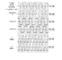
- Figs. 4A-4F present a series of signal timing diagrams depicting the sequential transformations that a representative filtered IF signal undergoes when processed in accordance with the signal processing operations shown in Fig. 3.
- Figs. 4A-4F present a series of signal timing diagrams depicting the sequential transformations that a representative filtered IF signal undergoes when processed in accordance with the signal processing operations shown in Fig. 3.
- dashed vertical synchronization lines occurring every 1 ⁇ 4 cycle (i.e., the examples assume sampling at four times the IF signal frequency) are used to correlate the respective signals in time and solid dots, at the intersection of the vertical synchronization lines and the signals they intersect, represent signal sample points (i.e., samples taken at four times the IF frequency).
- an RF frequency signal is received and downconverted by an RF tuner and passed though a bandpass filtered to produce a bandpass filtered IF signal (operation 310).
- a representative embodiment of such a bandpass filtered IF signal is presented in Fig. 4A.
- Such a representative signal is not limited to any specific intermediate frequency or to any specific waveform or type of modulation.
- the downconversion techniques of the present invention may be used to downconvert signals at IF frequencies significantly higher than the IF frequencies supported by circuits which do require the use of an A/D converter.
- the bandpass IF waveform is then passed through a zero-crossing comparator to generate a hard-limited IF signal (operation 312).
- a representative embodiment of a hard-limited IF signal generated as a result of operation 312 is presented in Fig. 4B.
- the generated signal is still a continuous signal of the same frequency as the input signal, but its amplitude has been converted to one of two logical states (e.g., 1 and -1).
- the hard-limited IF waveform is sampled at a sampling frequency which is the product of the intermediate frequency and an even integer number greater than or equal to four. For example, if the IF is 455kHz and a sampling rate of four times the intermediate frequency is used, the hard-limited signal is sampled at 1820 KHz, thereby producing four samples per signal cycle.
- representative samples taken at four times IF are depicted in Fig. 4B as solid dots at the intersection of the vertical synchronization lines and the signals they intersect. Although presented within the context of Fig. 4B, once sampled, the generated signal is no longer a continuous, signal. It has been converted to a series of two-state logical samples, representative of the received, continuous hard-limited signal.
- the hard-limited IF samples are then processed using two separate transformation processes to generate I and Q component samples (operation 316).
- the hard-limited IF samples shown in Fig. 4B are logically multiplied by 1, 0, -1, 0 to generate I component samples.
- Hard-limited IF samples are logically multiplied by 0, 1, 0, -1 to generate Q component samples. Representative embodiments of the resulting I and Q component samples are presented in Fig. 4E and Fig. 4F, respectively.
- the respective I and Q values represented may be validated by visually multiplying each hard-limited sampled value represented in Fig. 4B by the sampled values of cos(2 ⁇ f 0 *t), as depicted in Fig. 4C, to obtain each I sample represented in Fig. 4E, and multiplying each hard-limited sampled value represented in Fig. 4B by the sampled values of sin(2 ⁇ f 0 *t), as depicted in Fig. 4D, to obtain each Q sample represented in Fig. 4F.
- I and Q component samples can be optionally reduced, without adversely affecting subsequent information processing, by decimating the I and Q sample sequences by an odd integer, as previously discussed.
- This optional decimation process (represented in Fig. 3, as step 318, with dashed lines) may be performed for several advantageous reasons such as to reduce processing loads associated with the subsequent low-pass filtering.
- the I and Q samples presented in Figs. 4E and 4F have been marked with an "x" to illustrate the samples that would be eliminated if the respective I and Q samples were to be decimated by three (upper row) and decimated by five (lower row), respectively.
- an equal number of correlated samples are eliminated from both the I and Q components to assure symmetric processing of I and Q components in subsequent processing steps and to avoid loss of I and Q phase information.
- the number of samples per IF frequency cycle must be relatively prime to the decimation value. For example, if a signal is sampled at four times the input signal IF frequency, three and five are appropriate decimation values for four-and-three and four-and-five are relatively prime. Likewise, if a signal is sampled at eight times the input signal IF frequency, three and five are also appropriate decimation values for eight-and-three and eight-and-five are relatively prime. If a signal is sampled at twelve times the input signal IF frequency, however, five remains an appropriate decimation values for twelve and five are relatively prime, but three is no longer an appropriate decimation values, since twelve and three are not relatively prime.
- I and Q samples are optionally decimated, low-pass filtering of the I and Q component samples is next performed (operation 320) using up/down counters to integrate the respective I and Q components by summing I and Q component sample values over a period of time equal to the bit period.
- both I and Q counters can be optionally right shifted (i.e., divided by a multiple of two), as depicted in optional operation 322, to assure that the largest value remains below the upper range of the respective up/down counters and/or to allow the summed values to be represented within a fixed number of bits without loosing I and Q phase information.
- Figs. 5A-5F, Figs. 6A-6F and Figs. 7A-7F present signal timing diagrams that are identical in nature to Figs. 4A-4F, with the exception that while the IF signal in Figs. 4A, 4B, 4E and 4F depict signals with a phase of -45 degrees relative to a local IF signal cos(2 ⁇ f o *t), Figs.
- Figs 6A, 6B, 6E and 6F and 7A, 7B, 7E and 7F represent signals with relative phases of +45 degrees, -135 degrees and +135 degrees, respectively.
- the phase of the received IF signal significantly affects the I and Q values generated.
- the summed values generated from I or Q samples over a bit period will also be significantly affected by the phase of the received IF signal.
- summation of the approximately 1137 samples associated with the generated I component samples, a subset of which are depicted in Fig. 4E, will result in a large positive number.
- a signal in quadrant I i.e., with a phase between 0 degrees (alternately represented as 360 degrees) and +90 degrees (alternately represented as -270 degrees)
- a signal in quadrant I i.e., a signal with a phase between +90 degrees and +180(alternately represented as -270 degrees)
- a signal in quadrant I i.e., a signal with a phase between +90 degrees and +180(alternately represented as -270 degrees)
- a signal in quadrant I i.e., a signal with a phase between +90 degrees and +180(alternately represented as -270 degrees)
- a signal in quadrant IV i.e., with a phase between 0 degrees (alternately represented as 360 degrees) and -90 degrees (alternately represented as +270 degrees)
- a signal in quadrant III i.e., a signal with a phase between -90 degrees and -180(alternately represented as +180 degrees)
- a signal in quadrant III i.e., a signal with a phase between -90 degrees and -180(alternately represented as +180 degrees)
- a signal in quadrant III i.e., a signal with a phase between -90 degrees and -180(alternately represented as +180 degrees)
- any signal with a phase other that 0 degrees (i.e., 360 degrees), 90 degrees (i.e., -270 degrees), 180 degrees (i.e., -180 degrees) or -90 degrees (i.e., +270), will have very large positive or negative I and Q values (i.e., the magnitude of the values will be approximately one-half the number of samples/bit period remaining at the time of summation, even if optional decimation is used.)
- the only phase at which the I and Q sums would not equal the maximum possible magnitude would occur at the quadrant boundaries.
- phase of the signal can be identified as being in only one of eight states (i.e., within one of the four quadrants, or precisely upon one of the four quadrant boundaries, as previously described).
- noise exists in all real operational environments and systems, and with respect to the teachings of the present invention, noise inherent in the received signal allows the phase of a received signal to be more precisely resolved than would be possible in a noiseless case.
- noise will result in some fraction of the individual Q component samples included in the value summed for the bit period, to be negative or zero, when in the noiseless case the same values would all have been positive.
- the summed Q value will still be positive, but it will not be as large as it would have been in the noiseless case.
- the DSP may be calibrated to provide a close estimate of the Q value based upon the actual value of the Q sum generated.
- the value of Q can be more precisely estimated for signal phases that (referring to Fig. 8) lay within 45 degrees of the border between quadrant I and quadrant IV, and within 45 degrees of the border between quadrant II and quadrant III (i.e., for signal with phases between ⁇ 45 degrees and ⁇ 135 degrees).
- the value of I can be more precisely estimated for signal phases which (referring again to Fig. 8) lay within 45 degrees of the border between quadrant I and quadrant II, and within 45 degrees of the border between quadrant III and quadrant IV (i.e., for signal with phases between +45 and +135 degrees and -45 and -135 degrees).
- a digital signal processor evaluates the summed I and Q value pairs to determine the signal phase for each bit period. The phase for bit period N is then compared to the phase for bit period N-1. If the difference between the signal phases calculated for N and N-1 is closer to zero degrees than 180 degrees, the digital signal process assigns one logical value (e.g., 0) to the demodulated signal. If the difference between the signal phases calculated for N and N-1 is closer to 180 degrees than zero degrees, the digital signal process assigns the opposite logical value (e.g., 1) to the demodulated signal.
- BDPSK Binary Phase Shift Keying
- teachings of the present invention are also applicable to other signal modulation techniques in which signal phase, or changes in signal phase are used to encode information.
- the teachings of the present invention can be used to demodulated Frequency Shift Keying (FSK) and differential FSK modulated signals.
- FSK Frequency Shift Keying
- PSK Phase Shift Keying
- Such modulation techniques differ from the Phase Shift Keying (PSK) modulation techniques, addressed above, in that the signal rotates in phase during the bit period rather than staying constant as in PSK. For example, if the deviation in a FSK signal is set to greater than .5, the phase will rotate more than 90 degrees in a bit period and appear in two quadrants.
- the digital signal processor will interpret a shift in the positive direction as one logical value (e.g., 1) and will interpret a shift in the negative direction as another logical value (e.g., 0). If the deviation in a FSK signal is set to greater than 1, the phase will rotate more than 180 degrees in a bit period and appear in three quadrants.
- the digital signal processor will interpret a shift in the positive direction as one logical value (e.g., 1) and will interpret a shift in the positive direction as another logical value (e.g., 0).
- phase vector is no longer quantized to very few states (such as the eight associated with PSK in a noiseless environment), for the time that the signal spends in each quadrant determines the average phase angle, because the average number of I counts and Q counts per bit is proportional to the time that I and Q spend in each quadrant.
- the deviation in a FSK signal is set to greater than 1 (i.e., that phase will rotate more than 180 degrees in a bit period and appear in three quadrants) and that the phase calculated for the last bit period was -10 degrees. If, during the following bit period, the signal were to swing in the positive direction, the I and Q components would pass through 10 degrees of quadrant IV, 90 degrees of quadrant I, and 80 degrees of quadrant II. Such a change in signal phase over the duration of the bit period would be captured in each of the respective I and Q samples contributing to the respective I and Q sums over the bit period. With respect to the Q component, 170 out of 180 degrees will result in positive Q component samples while 10 out of 180 will result in negative Q values.
- the value of Q can be expected to be a relatively high positive number (i.e., in the case of 1375 samples per bit period, with no decimation, approximately (170/180 x 1375/2) - (10/180 x 1375/2) ⁇ +610).
- the value of I can be expected to be a relatively low positive number (i.e., in the case of 1375 samples per bit period, with no decimation, approximately (100/180 x 1375/2) - (80/180 x 1375/2) ⁇ +76).
- phase calculated for the last bit period was -10 degrees, but during the following bit period the signal swings in the negative direction.
- the I and Q components would pass through 80 degrees of quadrant IV, 90 degrees of quadrant III, and 10 degrees of quadrant II.
- 170 out of 180 degrees will result in negative Q component samples while 10 out of 180 will result in positive Q values, as a result, the value of Q can be expected to be a relatively high negative number (i.e., in the case of 1375 samples per bit period, with no decimation, approximately -(170/180 x 1375/2) + (10/180 x 1375/2) ⁇ -610).
- the value of I can be expected to be a relatively low negative number (i.e., in the case of 1375 samples per bit period, with no decimation, -(100/180 x 1375/2) + (80/180 x 1375/2) ⁇ -76).
- Similar application of the teachings of the present invention can be implemented within a DSP, or similar device, to demodulate virtually any phase or phase shift modulated signal.
- the phase of the IF input signal relative to a local IF signal can be resolved to within ninety degrees, in accordance with the teaching of the present invention, using a sampling rate of four times the IF input signal frequency.
- the phase of the IF input signal can be resolved to any practical resolution desired by increasing the sampling rate. For example, by increasing the sampling rate from four to eight samples per IF cycle, the phase resolution of an IF input signal can be reduced from 90 degrees to 45 degrees, without adding noise or dithering.
- Figs. 9-11 address a third non-limiting representative technique in which resolution of 45 degrees is achieved by sampling at eight times the intermediate frequency. Greater resolution, however, could be achieved with the same technique using a higher sampling frequency which is also the product of the intermediate frequency and an even integer number greater than or equal to four.
- Figs. 9A-9F and Figs. 10A-10F present representative timing diagrams, similar to those presented in Figs. 4-7, depicting the processing of IF input signals, using a sampling rate of eight times (rather than four times) the IF input signal frequency and hard-limiting the local IF cosine and sine signals, as represented in Figs. 9C, 9D, 10C and 10D, respectively.
- the I and Q samples presented in Figs. 9E-9F and Figs. 10E-10F are generated using the same techniques described in relation to Figs. 4-7.
- the IF input signal samples are multiplied by repetitive sequences comprised only of successive 1's and -1's.
- I and Q samples in Figs. 9E and 9F are summed over the span of a single signal cycle (i.e., any eight consecutive samples), the resulting values are +8 and 0, respectively.
- the I and Q samples in Figs. 10E and 10F are summed over the span of a single signal cycle, the resulting values are -4 and -4, respectively.
- I and Q sums generated in accordance with the teachings of the present, invention, directly reflect the phase of the IF input signal relative to a local IF signal.
- Fig. 11 presents I and Q sums, summed over the span of a single signal cycle (i.e., any eight consecutive samples), generated for IF input signals with phases of 0, +45, +90, +135, ⁇ 180, -135, -90, and -45, respectively, relative to a local IF signal.
- shifting the input signal presented in Fig. 9 to the right by 1/8 cycle i.e., to +45 degrees
- the I output to go to +4
- the Q output to +4.
- Shifting the input signal presented in Fig. 9 to the right by 1/4 cycle i.e., to +90 degrees
- Fig. 11 presents I and Q sums, summed over the span of a single signal cycle (i.e., any eight consecutive samples), generated for IF input signals with phases of 0, +45, +90, +135, ⁇ 180, -135, -90, and -45, respectively, relative to a
- phase of an IF input signal relative to a local IF signal can be determined based upon the respective I and Q sums.
- the I and Q sums for the respective signal phases within a single cycle can be determined as described in relation to Fig. 11.
- the number of signal cycles per bit period can be determined by multiplying the input signal frequency times the bit period.
- the expected counter value resulting from counting the I and Q samples, respectively, over a single bit period therefore, is the number of cycles per bit period times each of the respective single cycle I and Q sums.
- the demodulation processor merely compares the dumped I and Q sums generated for a bit period with the expected sums associated with each of the possible signal phases, and selects the closest match.
- IF to baseband I and Q downconversion techniques known in the prior art are dramatically improved in several significant ways.
- the expensive, power-consuming A/D converter and associated AGC circuit are replaced with a low-cost, low-power, zero-crossing comparator by using a zero-crossing comparator to create a hard-limited signal at the IF signal frequency which is directly input to the digital section of a FPGA or ASIC or similar device.
- These 1-bit samples are used to form the I and Q signals, replacing conventional twelve-bit samples and dramatically reducing the gate complexity required for processing the signals.
- the complex twelve-bit multiplication operations which would ordinarily required complex gated logic to implement, can be reduced to simple gated logic.
- generated I and Q signal components can be significantly reduced by systematically eliminating paired samples in both the I and Q components, without loss of I/Q phase information. Decimation can be used to greatly reduce the effort to perform subsequent lowpass filtering of the I and Q component signals.
- I and Q component samples generated in accordance with the present invention consist solely of the values 1, 0 and -1
- low-pass filtering of generated I and Q signals typically performed in the prior art using multi-bit multiplication and addition operations implemented within FPGA or ASIC devices with heavy gate counts, can be performed with simple up/down counters.
- bit sync adjust feature allows programmable up/down counters to be coordinated so that tracking between I and Q bit periods and their respective I and Q input streams can be precisely controlled, based upon constant monitoring of previously generated I and Q output samples.
- an "n and cycle type" feature allows the number of input samples included within a single I and Q bit period duration to be automatically calculated and dynamically adjusted.
- bit sync adjust and the n and cycle type features allow programmable up/down counters to be optimally aligned with the hard-limited I and Q input streams regardless of dynamic fluctuations in input data rates and sampling rates employed, and other signal timing discrepancies, thereby optimizing the accuracy of the resulting low-pass filtered I and Q samples at baseband and allowing the disclosed downconversion techniques to be used in a wide variety of dynamic operational environments. Nevertheless, the bit sync adjust and the n and cycle type features are optional.
- the added complexity of programmable up/down counters and the bit sync adjust and the n and cycle type features may be omitted without detracting from the benefits associated with the downconversion techniques of the present invention.
- the present invention greatly simplifies a previously complex process and provides substantial savings with respect to implementation device complexity, cost, and power consumption. Furthermore, by eliminating the use of A/D converters, the present invention can be used to downconvert input signals at intermediate frequencies that far exceed the processing speed of multi-bit A/D converters typically employed with traditional IF downconversion techniques.
- the present invention allows as much of the IF to baseband down conversion process as possible to be conducted in the digital realm. As a result, the processing techniques associated with the present invention can be implemented using discrete digital logic, implemented as a single low-cost integrated circuit produced as a stand-alone chip, or combined with additional integrated circuitry as part of a more complex chip. Regardless of the physical embodiment, the present invention allows provides a highly effective means for providing IF to baseband conversion for a wide range of phase modulated and frequency modulated signals.
- the present invention offers a very inexpensive and cost effective IF to baseband down conversion solution applicable to most phase and frequency modulated systems including a wide range of devices including radios, cell phones, two-way transceivers, pagers, transponders and other devices. If the signal to noise is positive (i.e., the signal is above the noise) the present invention can be used with no signal loss. If the signal is below the noise, the hard-limited approach discussed in this application will suffer only up to a 1db loss. In applications where such performance is operationally acceptable, the present invention offers numerous cost and performance advantages.
- a processor designed in accordance with the present invention can operate at high data rates due to its simple processing and small number of gates. The approach can be used in military radios as part of a FSK, PSK, DPSK, or similar frequency or phase demodulation system.
Landscapes
- Engineering & Computer Science (AREA)
- Power Engineering (AREA)
- Computer Networks & Wireless Communication (AREA)
- Signal Processing (AREA)
- Digital Transmission Methods That Use Modulated Carrier Waves (AREA)
- Superheterodyne Receivers (AREA)
- Transmitters (AREA)
- Input Circuits Of Receivers And Coupling Of Receivers And Audio Equipment (AREA)
- Burglar Alarm Systems (AREA)
- Analogue/Digital Conversion (AREA)
Applications Claiming Priority (2)
| Application Number | Priority Date | Filing Date | Title |
|---|---|---|---|
| US62522 | 1987-06-12 | ||
| US10/062,522 US7061998B1 (en) | 2002-02-05 | 2002-02-05 | Methods and apparatus for downconverting signals from intermediate frequency to baseband |
Publications (3)
| Publication Number | Publication Date |
|---|---|
| EP1339167A2 true EP1339167A2 (fr) | 2003-08-27 |
| EP1339167A3 EP1339167A3 (fr) | 2004-09-22 |
| EP1339167B1 EP1339167B1 (fr) | 2009-09-02 |
Family
ID=27658575
Family Applications (1)
| Application Number | Title | Priority Date | Filing Date |
|---|---|---|---|
| EP03001939A Expired - Lifetime EP1339167B1 (fr) | 2002-02-05 | 2003-01-30 | Dispositif convertisseur de signaux de fréquence intermédiaire en signaux de bande de base, et procédé |
Country Status (4)
| Country | Link |
|---|---|
| US (1) | US7061998B1 (fr) |
| EP (1) | EP1339167B1 (fr) |
| AT (1) | ATE441968T1 (fr) |
| DE (1) | DE60329045D1 (fr) |
Cited By (3)
| Publication number | Priority date | Publication date | Assignee | Title |
|---|---|---|---|---|
| WO2005067244A1 (fr) * | 2003-12-23 | 2005-07-21 | Infineon Technologies Ag | Procede et dispositif de demodulation d'un signal a modulation de phase |
| EP1720309A1 (fr) * | 2005-05-04 | 2006-11-08 | STMicroelectronics (Rousset) SAS | Dispositif de réception numérique |
| US7656932B2 (en) | 2005-05-04 | 2010-02-02 | Stmicroelectronics (Rousset) Sas | Digital receiver device |
Families Citing this family (8)
| Publication number | Priority date | Publication date | Assignee | Title |
|---|---|---|---|---|
| JP4657662B2 (ja) * | 2004-09-10 | 2011-03-23 | ルネサスエレクトロニクス株式会社 | クロックアンドデータリカバリ回路 |
| JP2006148627A (ja) * | 2004-11-22 | 2006-06-08 | Fujitsu Ltd | 周波数変調信号の復調器、および周波数変調信号の復調方法 |
| US8179296B2 (en) | 2005-09-30 | 2012-05-15 | The Massachusetts Institute Of Technology | Digital readout method and apparatus |
| US20100226495A1 (en) | 2007-10-29 | 2010-09-09 | Michael Kelly | Digital readout method and apparatus |
| US8471761B1 (en) | 2010-04-23 | 2013-06-25 | Akela, Inc. | Wideband radar nulling system |
| US8605853B2 (en) | 2011-07-01 | 2013-12-10 | Massachusetts Institute Of Technology | Methods and apparatus for in-pixel filtering in focal plane arrays |
| GB2523108A (en) * | 2014-02-12 | 2015-08-19 | Canon Kk | Frame synchronization at low ADC resolution |
| US10746851B2 (en) * | 2015-12-18 | 2020-08-18 | Texas Instruments Incorporated | Circuits and methods for determining chirp signal linearity and phase noise of a FMCW radar |
Citations (4)
| Publication number | Priority date | Publication date | Assignee | Title |
|---|---|---|---|---|
| US4669095A (en) * | 1985-09-27 | 1987-05-26 | Motorola, Inc. | Maximum distance from zero crossing MSK demodulator |
| US5640427A (en) * | 1993-11-18 | 1997-06-17 | Dsp Telecommunications Ltd. | Demodulator |
| US5696796A (en) * | 1995-06-07 | 1997-12-09 | Comsat Corporation | Continuously variable if sampling method for digital data transmission |
| WO2001019047A1 (fr) * | 1999-09-02 | 2001-03-15 | Koninklijke Philips Electronics N.V. | Recepteur d'interpolation de phase pour signaux rf a modulation angulaire |
Family Cites Families (5)
| Publication number | Priority date | Publication date | Assignee | Title |
|---|---|---|---|---|
| US4555667A (en) | 1983-09-26 | 1985-11-26 | Rixon, Inc. | Synchronous digital QPSK demodulator with carrier error correction |
| US5272448A (en) | 1991-11-20 | 1993-12-21 | Numa Technologies, Inc. | Method and apparatus to perform digital demodulation by measuring periods between zero crossings |
| US5159281A (en) | 1991-11-20 | 1992-10-27 | Nsi Partners | Digital demodulator using numerical processor to evaluate period measurements |
| US5539776A (en) | 1993-11-24 | 1996-07-23 | At&T Corp. | All digital if-to-baseband signal converter |
| US5633895A (en) | 1995-08-03 | 1997-05-27 | Motorola, Inc. | Communication device with synchronized zero-crossing demodulator and method |
-
2002
- 2002-02-05 US US10/062,522 patent/US7061998B1/en active Active
-
2003
- 2003-01-30 EP EP03001939A patent/EP1339167B1/fr not_active Expired - Lifetime
- 2003-01-30 AT AT03001939T patent/ATE441968T1/de not_active IP Right Cessation
- 2003-01-30 DE DE60329045T patent/DE60329045D1/de not_active Expired - Fee Related
Patent Citations (4)
| Publication number | Priority date | Publication date | Assignee | Title |
|---|---|---|---|---|
| US4669095A (en) * | 1985-09-27 | 1987-05-26 | Motorola, Inc. | Maximum distance from zero crossing MSK demodulator |
| US5640427A (en) * | 1993-11-18 | 1997-06-17 | Dsp Telecommunications Ltd. | Demodulator |
| US5696796A (en) * | 1995-06-07 | 1997-12-09 | Comsat Corporation | Continuously variable if sampling method for digital data transmission |
| WO2001019047A1 (fr) * | 1999-09-02 | 2001-03-15 | Koninklijke Philips Electronics N.V. | Recepteur d'interpolation de phase pour signaux rf a modulation angulaire |
Cited By (6)
| Publication number | Priority date | Publication date | Assignee | Title |
|---|---|---|---|---|
| WO2005067244A1 (fr) * | 2003-12-23 | 2005-07-21 | Infineon Technologies Ag | Procede et dispositif de demodulation d'un signal a modulation de phase |
| EP1720309A1 (fr) * | 2005-05-04 | 2006-11-08 | STMicroelectronics (Rousset) SAS | Dispositif de réception numérique |
| FR2885467A1 (fr) * | 2005-05-04 | 2006-11-10 | St Microelectronics Rousset | Dispositif de reception numerique base sur un comparateur en entree |
| US7656932B2 (en) | 2005-05-04 | 2010-02-02 | Stmicroelectronics (Rousset) Sas | Digital receiver device |
| US7660341B2 (en) | 2005-05-04 | 2010-02-09 | Stmicroelectronics (Rousset) Sas | Receiver device suited to a transmission system using a direct sequence spread spectrum |
| US7660342B2 (en) | 2005-05-04 | 2010-02-09 | Stmicroelectronics (Rousset) Sas | Digital receiver device based on an input comparator |
Also Published As
| Publication number | Publication date |
|---|---|
| EP1339167B1 (fr) | 2009-09-02 |
| DE60329045D1 (de) | 2009-10-15 |
| EP1339167A3 (fr) | 2004-09-22 |
| ATE441968T1 (de) | 2009-09-15 |
| US7061998B1 (en) | 2006-06-13 |
Similar Documents
| Publication | Publication Date | Title |
|---|---|---|
| CA2007149C (fr) | Convertisseur abaisseur a filtrage numerique par transformation de hilbert | |
| EP0804847B1 (fr) | RECEPTEUR DE SIGNAUX M-aires FSK | |
| JP2511206B2 (ja) | Gmsk信号復調方法及びその装置 | |
| US6094450A (en) | Spread spectrum chip shift keying modulation/demodulation system and method | |
| EP1339167B1 (fr) | Dispositif convertisseur de signaux de fréquence intermédiaire en signaux de bande de base, et procédé | |
| JPH07170210A (ja) | スペクトラム拡散変復調方法及びそれを用いた変調器・ 復調器 | |
| US5640427A (en) | Demodulator | |
| US6265948B1 (en) | Image rejection in logic-based architecture for FSK modulation and demodulation | |
| US8223909B2 (en) | Digital sampling apparatuses and methods | |
| US6549588B2 (en) | Communications system and corresponding receiver unit | |
| CN102368690A (zh) | 微纳卫星测控数字中频与基带处理方法及装置 | |
| US20070024477A1 (en) | DPSK demodulator and method | |
| US6288618B1 (en) | Logic-based architecture for FSK modulation and demodulation | |
| JP3917637B2 (ja) | 無線通信システム、無線送信機、無線受信機および無線通信方法 | |
| WO2001071931A2 (fr) | Syntoniseur numerique a frequence d'horloge optimisee, filtre cic parallele integre et oscillateur local | |
| US6002721A (en) | Carrier frequency estimator for a signal receiver | |
| JPH0621992A (ja) | 復調器 | |
| JP3489493B2 (ja) | シンボル同期装置および周波数ホッピング受信装置 | |
| EP1220504B1 (fr) | Démodulation de signaux MDF | |
| KR100959229B1 (ko) | 데이터 수신 장치 | |
| CN1066870C (zh) | 直接变频接收机 | |
| EP0620666B1 (fr) | Système de modulation differentiell à phase continue pour environnement de propagation à trajets multiples | |
| JPH07177054A (ja) | ディジタル無線通信端末 | |
| JP3452855B2 (ja) | データ受信装置 | |
| JPH06197090A (ja) | データ送受信装置 |
Legal Events
| Date | Code | Title | Description |
|---|---|---|---|
| PUAI | Public reference made under article 153(3) epc to a published international application that has entered the european phase |
Free format text: ORIGINAL CODE: 0009012 |
|
| AK | Designated contracting states |
Designated state(s): AT BE BG CH CY CZ DE DK EE ES FI FR GB GR HU IE IT LI LU MC NL PT SE SI SK TR |
|
| AX | Request for extension of the european patent |
Extension state: AL LT LV MK RO |
|
| PUAL | Search report despatched |
Free format text: ORIGINAL CODE: 0009013 |
|
| AK | Designated contracting states |
Kind code of ref document: A3 Designated state(s): AT BE BG CH CY CZ DE DK EE ES FI FR GB GR HU IE IT LI LU MC NL PT SE SI SK TR |
|
| AX | Request for extension of the european patent |
Extension state: AL LT LV MK RO |
|
| 17P | Request for examination filed |
Effective date: 20050322 |
|
| AKX | Designation fees paid |
Designated state(s): AT BE BG CH CY CZ DE DK EE ES FI FR GB GR HU IE IT LI LU MC NL PT SE SI SK TR |
|
| 17Q | First examination report despatched |
Effective date: 20080215 |
|
| GRAP | Despatch of communication of intention to grant a patent |
Free format text: ORIGINAL CODE: EPIDOSNIGR1 |
|
| GRAS | Grant fee paid |
Free format text: ORIGINAL CODE: EPIDOSNIGR3 |
|
| GRAA | (expected) grant |
Free format text: ORIGINAL CODE: 0009210 |
|
| AK | Designated contracting states |
Kind code of ref document: B1 Designated state(s): AT BE BG CH CY CZ DE DK EE ES FI FR GB GR HU IE IT LI LU MC NL PT SE SI SK TR |
|
| REG | Reference to a national code |
Ref country code: CH Ref legal event code: EP |
|
| REG | Reference to a national code |
Ref country code: IE Ref legal event code: FG4D |
|
| REF | Corresponds to: |
Ref document number: 60329045 Country of ref document: DE Date of ref document: 20091015 Kind code of ref document: P |
|
| PG25 | Lapsed in a contracting state [announced via postgrant information from national office to epo] |
Ref country code: SE Free format text: LAPSE BECAUSE OF FAILURE TO SUBMIT A TRANSLATION OF THE DESCRIPTION OR TO PAY THE FEE WITHIN THE PRESCRIBED TIME-LIMIT Effective date: 20090902 Ref country code: FI Free format text: LAPSE BECAUSE OF FAILURE TO SUBMIT A TRANSLATION OF THE DESCRIPTION OR TO PAY THE FEE WITHIN THE PRESCRIBED TIME-LIMIT Effective date: 20090902 |
|
| NLV1 | Nl: lapsed or annulled due to failure to fulfill the requirements of art. 29p and 29m of the patents act | ||
| PG25 | Lapsed in a contracting state [announced via postgrant information from national office to epo] |
Ref country code: SI Free format text: LAPSE BECAUSE OF FAILURE TO SUBMIT A TRANSLATION OF THE DESCRIPTION OR TO PAY THE FEE WITHIN THE PRESCRIBED TIME-LIMIT Effective date: 20090902 Ref country code: NL Free format text: LAPSE BECAUSE OF FAILURE TO SUBMIT A TRANSLATION OF THE DESCRIPTION OR TO PAY THE FEE WITHIN THE PRESCRIBED TIME-LIMIT Effective date: 20090902 |
|
| PG25 | Lapsed in a contracting state [announced via postgrant information from national office to epo] |
Ref country code: CY Free format text: LAPSE BECAUSE OF FAILURE TO SUBMIT A TRANSLATION OF THE DESCRIPTION OR TO PAY THE FEE WITHIN THE PRESCRIBED TIME-LIMIT Effective date: 20090902 |
|
| PG25 | Lapsed in a contracting state [announced via postgrant information from national office to epo] |
Ref country code: PT Free format text: LAPSE BECAUSE OF FAILURE TO SUBMIT A TRANSLATION OF THE DESCRIPTION OR TO PAY THE FEE WITHIN THE PRESCRIBED TIME-LIMIT Effective date: 20100104 Ref country code: ES Free format text: LAPSE BECAUSE OF FAILURE TO SUBMIT A TRANSLATION OF THE DESCRIPTION OR TO PAY THE FEE WITHIN THE PRESCRIBED TIME-LIMIT Effective date: 20091213 Ref country code: EE Free format text: LAPSE BECAUSE OF FAILURE TO SUBMIT A TRANSLATION OF THE DESCRIPTION OR TO PAY THE FEE WITHIN THE PRESCRIBED TIME-LIMIT Effective date: 20090902 Ref country code: CZ Free format text: LAPSE BECAUSE OF FAILURE TO SUBMIT A TRANSLATION OF THE DESCRIPTION OR TO PAY THE FEE WITHIN THE PRESCRIBED TIME-LIMIT Effective date: 20090902 |
|
| PG25 | Lapsed in a contracting state [announced via postgrant information from national office to epo] |
Ref country code: SK Free format text: LAPSE BECAUSE OF FAILURE TO SUBMIT A TRANSLATION OF THE DESCRIPTION OR TO PAY THE FEE WITHIN THE PRESCRIBED TIME-LIMIT Effective date: 20090902 |
|
| PG25 | Lapsed in a contracting state [announced via postgrant information from national office to epo] |
Ref country code: BE Free format text: LAPSE BECAUSE OF FAILURE TO SUBMIT A TRANSLATION OF THE DESCRIPTION OR TO PAY THE FEE WITHIN THE PRESCRIBED TIME-LIMIT Effective date: 20090902 Ref country code: AT Free format text: LAPSE BECAUSE OF FAILURE TO SUBMIT A TRANSLATION OF THE DESCRIPTION OR TO PAY THE FEE WITHIN THE PRESCRIBED TIME-LIMIT Effective date: 20090902 |
|
| PLBE | No opposition filed within time limit |
Free format text: ORIGINAL CODE: 0009261 |
|
| STAA | Information on the status of an ep patent application or granted ep patent |
Free format text: STATUS: NO OPPOSITION FILED WITHIN TIME LIMIT |
|
| PG25 | Lapsed in a contracting state [announced via postgrant information from national office to epo] |
Ref country code: DK Free format text: LAPSE BECAUSE OF FAILURE TO SUBMIT A TRANSLATION OF THE DESCRIPTION OR TO PAY THE FEE WITHIN THE PRESCRIBED TIME-LIMIT Effective date: 20090902 |
|
| 26N | No opposition filed |
Effective date: 20100603 |
|
| PG25 | Lapsed in a contracting state [announced via postgrant information from national office to epo] |
Ref country code: MC Free format text: LAPSE BECAUSE OF NON-PAYMENT OF DUE FEES Effective date: 20100131 |
|
| REG | Reference to a national code |
Ref country code: CH Ref legal event code: PL |
|
| GBPC | Gb: european patent ceased through non-payment of renewal fee |
Effective date: 20100130 |
|
| REG | Reference to a national code |
Ref country code: FR Ref legal event code: ST Effective date: 20100930 |
|
| PG25 | Lapsed in a contracting state [announced via postgrant information from national office to epo] |
Ref country code: LI Free format text: LAPSE BECAUSE OF NON-PAYMENT OF DUE FEES Effective date: 20100131 Ref country code: GR Free format text: LAPSE BECAUSE OF FAILURE TO SUBMIT A TRANSLATION OF THE DESCRIPTION OR TO PAY THE FEE WITHIN THE PRESCRIBED TIME-LIMIT Effective date: 20091203 Ref country code: FR Free format text: LAPSE BECAUSE OF NON-PAYMENT OF DUE FEES Effective date: 20100201 Ref country code: CH Free format text: LAPSE BECAUSE OF NON-PAYMENT OF DUE FEES Effective date: 20100131 |
|
| PG25 | Lapsed in a contracting state [announced via postgrant information from national office to epo] |
Ref country code: DE Free format text: LAPSE BECAUSE OF NON-PAYMENT OF DUE FEES Effective date: 20100803 |
|
| PG25 | Lapsed in a contracting state [announced via postgrant information from national office to epo] |
Ref country code: GB Free format text: LAPSE BECAUSE OF NON-PAYMENT OF DUE FEES Effective date: 20100130 |
|
| PG25 | Lapsed in a contracting state [announced via postgrant information from national office to epo] |
Ref country code: IE Free format text: LAPSE BECAUSE OF NON-PAYMENT OF DUE FEES Effective date: 20100130 |
|
| PG25 | Lapsed in a contracting state [announced via postgrant information from national office to epo] |
Ref country code: IT Free format text: LAPSE BECAUSE OF FAILURE TO SUBMIT A TRANSLATION OF THE DESCRIPTION OR TO PAY THE FEE WITHIN THE PRESCRIBED TIME-LIMIT Effective date: 20090902 |
|
| PG25 | Lapsed in a contracting state [announced via postgrant information from national office to epo] |
Ref country code: HU Free format text: LAPSE BECAUSE OF FAILURE TO SUBMIT A TRANSLATION OF THE DESCRIPTION OR TO PAY THE FEE WITHIN THE PRESCRIBED TIME-LIMIT Effective date: 20100303 Ref country code: BG Free format text: LAPSE BECAUSE OF FAILURE TO SUBMIT A TRANSLATION OF THE DESCRIPTION OR TO PAY THE FEE WITHIN THE PRESCRIBED TIME-LIMIT Effective date: 20090902 Ref country code: LU Free format text: LAPSE BECAUSE OF NON-PAYMENT OF DUE FEES Effective date: 20100130 |
|
| PG25 | Lapsed in a contracting state [announced via postgrant information from national office to epo] |
Ref country code: TR Free format text: LAPSE BECAUSE OF FAILURE TO SUBMIT A TRANSLATION OF THE DESCRIPTION OR TO PAY THE FEE WITHIN THE PRESCRIBED TIME-LIMIT Effective date: 20090902 |