EP1333366A1 - Touch panel capable of wide-area inputting - Google Patents
Touch panel capable of wide-area inputting Download PDFInfo
- Publication number
- EP1333366A1 EP1333366A1 EP01979003A EP01979003A EP1333366A1 EP 1333366 A1 EP1333366 A1 EP 1333366A1 EP 01979003 A EP01979003 A EP 01979003A EP 01979003 A EP01979003 A EP 01979003A EP 1333366 A1 EP1333366 A1 EP 1333366A1
- Authority
- EP
- European Patent Office
- Prior art keywords
- touch panel
- bus bars
- wide range
- transparent electrode
- input area
- Prior art date
- Legal status (The legal status is an assumption and is not a legal conclusion. Google has not performed a legal analysis and makes no representation as to the accuracy of the status listed.)
- Withdrawn
Links
Images







Classifications
-
- G—PHYSICS
- G06—COMPUTING OR CALCULATING; COUNTING
- G06F—ELECTRIC DIGITAL DATA PROCESSING
- G06F3/00—Input arrangements for transferring data to be processed into a form capable of being handled by the computer; Output arrangements for transferring data from processing unit to output unit, e.g. interface arrangements
- G06F3/01—Input arrangements or combined input and output arrangements for interaction between user and computer
- G06F3/03—Arrangements for converting the position or the displacement of a member into a coded form
- G06F3/041—Digitisers, e.g. for touch screens or touch pads, characterised by the transducing means
- G06F3/045—Digitisers, e.g. for touch screens or touch pads, characterised by the transducing means using resistive elements, e.g. a single continuous surface or two parallel surfaces put in contact
-
- G—PHYSICS
- G06—COMPUTING OR CALCULATING; COUNTING
- G06F—ELECTRIC DIGITAL DATA PROCESSING
- G06F3/00—Input arrangements for transferring data to be processed into a form capable of being handled by the computer; Output arrangements for transferring data from processing unit to output unit, e.g. interface arrangements
- G06F3/01—Input arrangements or combined input and output arrangements for interaction between user and computer
- G06F3/03—Arrangements for converting the position or the displacement of a member into a coded form
- G06F3/041—Digitisers, e.g. for touch screens or touch pads, characterised by the transducing means
-
- G—PHYSICS
- G06—COMPUTING OR CALCULATING; COUNTING
- G06K—GRAPHICAL DATA READING; PRESENTATION OF DATA; RECORD CARRIERS; HANDLING RECORD CARRIERS
- G06K11/00—Methods or arrangements for graph-reading or for converting the pattern of mechanical parameters, e.g. force or presence, into electrical signal
Definitions
- the present invention relates to a touch panel allowing a larger number of input operations over a wide area, in which an additional input section from which input operations can be executed may be formed in addition to a screen indicating input section from which input operations can be executed according to indications on a screen.
- Touch panels that have conventionally been used in electronic notepads, personal computers, and the like include ones of analog resistance film type.
- a touch panel of this type as shown in Fig. 11, ordinarily, two conductive panels 4, 5 having a pair of parallel bus bars 43, 53 and a transparent electrode 42, 52 formed between the bus bars 43, 53 on one surface of a transparent insulating base 41, 51 are made to face each other and are stuck together with use of a circumferential insulating adhesive layer 6 so that the bus bars 43 and 53 are arranged rectangularly.
- Each of the conductive panels 4 and 5 has a routing circuit 44, 54 connected to the bus bars.
- This touch panel is provided on a screen of an LCD (Liquid Crystal Display), a CRT (Cathode-Ray Tube), and the like, and is pressed by a finger, a pen or the like under indications displayed on the screen that can be seen through the transparent insulating bases 41 and 51 and the transparent electrodes 42 and 52 with the screen located on their rear side, so that continuity between the transparent electrodes 42 and 52 that are normally insulated from each other by a small space is made for position input.
- LCD Liquid Crystal Display
- CRT Cathode-Ray Tube
- the bus bars 43 and 53 and the routing circuits 44 and 54 are not transparent, and are therefore hidden behind a picture-frame-like housing or the like placed on a front surface of the touch panel that is placed on the screen.
- a picture-frame-like housing or the like placed on a front surface of the touch panel that is placed on the screen.
- an area in which the bus bars 43, 53 and the routing circuit 44, 54 are formed has been made as small as possible (narrow picture frame) and an area in which the transparent electrodes face each other has been enlarged.
- An object of the present invention is to solve the above-mentioned issues and to provide a touch panel allowing a larger number of input operations over a wide area, in which an additional input section from which input operations can be executed may be formed in addition to a screen indicating input section from which input operations can be executed according to indications on a screen.
- the present invention is configured as will be described below.
- a wide range-inputable touch panel of analog resistance film type comprising:
- a wide range-inputable touch panel of analog resistance film type as defined in the first aspect, wherein the first and the second routing circuits are provided on the first and the second conductive panels, respectively, and are connected to the first and the second bus bars, respectively.
- a wide range-inputable touch panel of analog resistance film type as defined in the first aspect, wherein the first and the second routing circuits are provided on the second conductive panel and are connected to the first and the second bus bars, respectively.
- a wide range-inputable touch panel as defined in any one of the first through third aspects, wherein an insulating interconnection overcoating layer is formed on a surface of the first conductive panel where the first routing circuit is formed or on a surface of the second conductive panel where the second routing circuit is formed, in an area that does not overlap portions of the bus bars on the surface which can be brought into electrical contact by a press with the facing transparent electrode and in an area including the routing circuit.
- a wide range-inputable touch panel of analog resistance film type as defined in any one of the first through third aspects, wherein the space sections are spaces formed in the adhesive layer cut out from an outer edge side thereof.
- a wide range-inputable touch panel of analog resistance film type as defined in the fourth aspect, wherein the space sections are spaces formed in the adhesive layer cut out from an outer edge side thereof.
- a wide range-inputable touch panel as defined in any one of the first through third aspects, wherein the space sections are spaces in which two or more cut-out sections formed in the adhesive layer cut out from an outer edge side thereof exist side by side along one side.
- a wide range-inputable touch panel as defined in the fourth aspect, wherein the space sections are spaces in which two or more cut-out sections formed in the adhesive layer cut out from an outer edge side thereof exist side by side along one side.
- a wide range-inputable touch panel as defined in the seventh aspect, wherein dot-like spacers are provided in the spaces.
- a wide range-inputable touch panel as defined in any one of the first through seventh aspects, wherein at least the one bus bar of the pair of bus bars is covered with carbon layers in cut-out sections of the adhesive layer.
- a wide range-inputable touch panel as defined in any one of the first through third aspects, wherein the space sections are punched holes extending through the adhesive layer.
- a wide range-inputable touch panel as defined in any one of the first through third aspects, wherein the adhesive layer 3 has a through hole formed corresponding to the first input area of the first transparent electrode and to the second input area of the second transparent electrode and has a partition section that partitions the through hole and the space sections.
- a wide range-inputable touch panel as defined in any one of the first through third aspects, wherein an ordinary input section as a region through which a screen placed under the touch panel can be seen for input operations is composed of the first input area of the first transparent electrode and of the second input area of the second transparent electrode that faces the first input area, and an additional input section different from the ordinary input section is composed of at least one bus bar of the pair of second bus bars and of the third input area of the first transparent electrode that faces at least the one bus bar.
- a wide range-inputable touch panel as defined in the 13th aspect, wherein the additional input section is composed of additional electrode sections that are connected through extension line sections to at least one bus bar of the pair of second bus bars, and the third input area of the first transparent electrode that faces the additional electrode sections through the space sections.
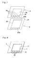
- Figs. 1 and 3 are an exploded perspective view showing a wide range-inputable touch panel according to the embodiment of the present invention and an exploded perspective view of the touch panel from which one conductive panel has been removed..
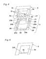
- Figs. 2 and 4 are an exploded perspective view showing a wide range-inputable touch panel according to a modification of the embodiment of the present invention and an exploded perspective view of the touch panel from which one conductive panel has been removed.
- Fig. 5 is a perspective view showing a shape of an adhesive layer that is formed in a wide range-inputable touch panel according to another modification of the embodiment of the present invention.
- Fig. 6 is an exploded perspective view showing a wide range-inputable touch panel according to still another modification of the embodiment of the present invention, from which one conductive panel has been removed.
- Fig. 7 is an exploded perspective view showing a wide range-inputable touch panel according to still another modification of the embodiment of the present invention, from which one conductive panel has been removed.
- Fig. 8 is a perspective view showing a housing provided on a front surface of a wide range-inputable touch panel according to still another modification of the embodiment of the present invention.
- Fig. 9 is a perspective view showing an example of a shape of an adhesive layer that is not formed in the wide range-inputable touch panel according to the embodiment of the present invention.
- Fig. 10 is a perspective view showing a shape of an adhesive layer that is formed in a wide range-inputable touch panel according to still another modification of the embodiment of the present invention.
- Fig. 11 is an exploded perspective view showing an example of a conventional touch panel.
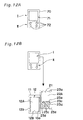
- Figs. 12A and 12B are a plan view and an exploded view showing a PDA equipped with a wide range-inputable touch panel according to still another embodiment of the present invention.
- Fig. 13 is an exploded view showing a PDA equipped with an example of a conventional touch panel.
- reference character 1 denotes a first conductive panel
- character 11 denotes a first transparent insulating base of the first conductive panel
- character 12 denotes a first transparent electrode on the first conductive panel
- characters 13a and 13b denote first bus bars on the first conductive panel
- characters 14a and 14b denote a first routing circuit on the first conductive panel
- character 2 denotes a second conductive panel
- character 21 denotes a second transparent insulating base of the second conductive panel
- character 22 denotes a second transparent electrode on the second conductive panel
- characters 23a and 23b denote second bus bars on the second conductive panel
- characters 24a and 24b denote a second routing circuit on the second conductive panel
- characters 25a and 25b denote a routing circuit
- character 26 denotes linkage sections
- character 27 denotes an interconnection overcoating layer
- character 28 denotes a carbon layer
- character 3 denotes an adhesive layer
- character 31 denotes a cut-out
- the first conductive panel 1 on a side for touch input in the touch panel shown in Fig. 1 has the pair of first bus bars 13a and 13b parallel to each other on one surface of the first transparent insulating base 11 and the first transparent electrode 12 formed between the first bus bars 13a and 13b and has the set of first routing circuit 14a and 14b connected to the first bus bars 13a and 13b in an insulated section outside the first transparent electrode 12.
- the first transparent electrode 12 is formed over a first input area 12A facing the second transparent electrode 22 of the second conductive panel 2 on a screen side that will be described below and over a third input area 12B facing one of the second bus bars 23a and 23b of the second conductive panel 2 on the screen side.
- the second conductive panel 2 on the screen side of the touch panel shown in Fig. 1 has the pair of second bus bars 23a and 23b parallel to each other on one surface of the second transparent insulating base 21 and the second transparent electrode 22 formed between the second bus bars 23a and 23b and has the set of second routing circuit 24a and 24b connected to the second bus bars 23a and 23b in an insulated section outside the second transparent electrode 22.
- the second transparent electrode 22 is formed over a second input area 22A between the second bus bars 23a and 23b.
- the first conductive panel 1 on the side for touch input and the second conductive panel 2 on the screen side are made to face each other so that the first and second bus bars 13a, 13b, 23a, and 23b are arranged rectangularly, and the panels are stuck together with use of the circumferential insulating adhesive layer 3 so that a space is formed between the first and second transparent electrode 12 and 22.
- the touch panel shown in Fig. 1 has the first input area 12A configuring an ordinary input section I that is to be pressed by a finger, a pen, or the like under directions displayed on the screen which can be seen through a central portion of the panel, and the third input area 12B configuring an additional input section II through which the screen can not be seen, in neighborhood of an edge of the touch panel, in addition to the first input area 12A.
- one second bus bar 23a on the second conductive panel 2 on the screen side and the third input area 12B of the first transparent electrode 12 on the first conductive panel 1 on the side for touch input which fronts the bus bar 23a through spaces (the cut-out sections 31) formed in the adhesive layer 3 cut out from an outer edge side thereof, face each other so as to be capable of making electrical contact with each other by a press and configure the additional input section II.
- input operations can be executed even on the second bus bar 23a that would be excluded from input areas in conventional panels, an input area of the panel is accordingly larger than in conventional panels, and a larger number of input operations can be executed with one display operation on the screen.
- the housing 7 as shown in Fig. 8 may be provided on the front surface of the touch panel so as to conceal the first and second bus bars 13a, 13b, 23a, and 23b and the first and second routing circuits 14a, 14b, 24a, and 24b.
- conventional input operations under directions displayed on the screen can be executed on the screen see-through input section 71 that opens in a central portion of the housing and, on the other hand, input operations on the above bus bar of the touch panel can be executed with presses on a plurality of button input sections 72 that are arranged corresponding to the plurality of cut-out sections 31 of the adhesive layer 3 and that use a portion of a main body of the housing 7.
- button input sections may be formed separately from the main body of the housing 7, by printing or the like on a portion of a surface of the touch panel that resides over the bus bar.
- the screen see-through input section 71 is a section that corresponds to the first input area 12A and to the second input area 22A
- the plurality of button input sections 72 are sections that correspond to the third input area 12B.
- one bus bar 23a on the second conductive panel 2 on the screen side performs a function as a switch.
- a configuration may be adopted in which any one of other three bus bars 13a, 13b, and 23b or two or more out of four bus bars 13a, 13b, 23a, and 23b, and the transparent electrodes on the conductive panels opposed to the bus bars through the spaces (the cut-out sections 31) formed in the adhesive layer 3 cut out from the outer edge side thereof face each other so as to be capable of making electrical contact with each other by a press.
- the first conductive panel 1 may be provided on a side of an upper electrode and the second conductive panel 2 may be provided on a side of a lower electrode (the side of the screen such as LCD). Or otherwise, the first conductive panel 1 may be provided on the side of the lower electrode (the side of the screen such as LCD) and the second conductive panel 2 may be provided on the side of the upper electrode.
- the wide range-inputable touch panel according to the embodiment of the present invention may have a configuration in which two sets of routing circuits are formed on one of the conductive panels.
- no routing circuits may be provided on the first conductive panel 1 on the side for touch input
- two sets of routing circuits 24a, 24b, 25a, and 25b may be provided collectively in the insulated section outside the transparent electrode 22 on the second conductive panel 2 on the screen side
- one set of routing circuit 25a and 25b out of the two sets may be configured so as to be connected indirectly and electrically to the first bus bars 13a and 13b on the first conductive panel 1 on the side for touch input, by way of conductive adhesive provided as the linkage sections 26 of the routing circuit across through holes 3a of the adhesive layer 3, and other configuration may be made the same as that of the touch panel shown in Fig. 1 (see Fig. 2).
- routing circuits are collectively formed on one of the conductive panels
- only one bus bar or only two bus bars on the conductive panel provided with both the routing circuits, and the transparent electrode on the conductive panel on the side opposed to the bus bars across the spaces formed in the adhesive layer cut out from the outer edge side thereof can be made to face each other so as to be brought into electrical contact with each other by a press, in contrast to the configuration in which one set of routing circuits is formed on each of the conductive panels. That is because it is difficult to provide input areas in the bus bars on the conductive panel on the side provided with no routing circuits, for the routing circuits and the linkage sections reside in positions that the bus bars on the panel on the opposite side face, as shown in Fig. 2.
- the routing circuits in the touch panel shown in Fig. 2 are gathered on the conductive panel 2 on the screen side.
- the routing circuits may be formed collectively on the conductive panel 1 on the side for touch input.
- the first transparent insulating base 11 of the first conductive panel 1 on the side for touch input which is required to have a flexibility for input operations, there are commonly used engineering plastic based on polycarbonate, polyamide, polyether ketone, and the like; transparent film based on acrylic resin, polyethylene terephthalate, polybutylene terephthalate, and the like; laminated body of those materials; and the like.
- the hard coat layer may be made from inorganic material such as siloxane-based resin or organic material such as thermosetting resin based on acrylic epoxy and urethane and acrylate-based photo-setting resin.
- Non-glare treatment for preventing light reflection may be applied to the surface of the first transparent insulating base 11 of the first conductive panel 1 on the side for touch input that is opposite to the surface having the first transparent electrode 12.
- the first transparent insulating base 11 and the hard coat layer may be subjected to roughening process, or minute particles such as extender pigment, silica, and alumina may be added into the hard coat layer.
- the second transparent insulating base 21 of the second conductive panel 2 on the screen side are used glass board such as soda glass, borosilicate glass, and tempered glass; and besides; engineering plastic based on polycarbonate, polyamide, polyether ketone, and the like; transparent resin plate or transparent film based on acrylic resin, polyethylene terephthalate, polybutylene terephthalate, and the like; laminated body of those materials; and the like.
- the first and second transparent insulating bases 1 and 2 of the conductive panels on the side for touch input and the screen side may not only have a function as supporting bodies for the transparent electrodes but may have another optical function and the like.
- a touch panel in which an antireflection filter of circular polarization type is provided has a configuration in which, at least, a first quarter-wave plate, two layers of transparent electrodes facing each other with spacers therebetween, a second quarter-wave plate having an optical axis orthogonal to an optical axis of the first quarter-wave plate, and a polarizing plate are arranged in order of mention from a side of a liquid crystal display.
- the first quarter-wave plate may be used as the transparent insulating base of the conductive panel on the screen side and the second quarter-wave plate may be used as the transparent insulating base of the conductive panel on the side for touch input.
- the above-mentioned quarter-wave plates are transparent resin plates or transparent films that have a function of converting linearly polarized light into circularly polarized light or generally circularly polarized light by causing temporal phase shift (phase difference) between two components of polarized light orthogonal to each other obtained from resolution of linearly polarized light and that have a function of delaying phase of one of the components of polarized light by a quarter of a wavelength thereof relative to incident light having a center wavelength (about 550 nm) of visible light region (about 400 nm to 700 nm).
- the transparent electrodes 12 and 22 can be obtained as transparent conductive films formed partially on the transparent insulating bases 11 and 21.
- Means for patterning the transparent conductive films include a method of removing an unnecessary portion of a transparent conductive film by resist etching after providing the transparent conductive film on an overall surface, a method of forming a pattern of a transparent conductive film with use of a metal mask, or the like.
- a transparent conductive film formed overall on a transparent insulating base may be covered partially with an insulating patterning layer, and then an exposed portion of the transparent conductive film may be obtained as one or both of the transparent electrodes 12 and 22.
- the transparent electrode of the conductive panel on which no routing circuits are formed may be obtained as a portion of the transparent conductive film formed overall on the transparent insulating base (not shown).
- Material of such a transparent conductive film may be metal oxide film of tin oxide, indium oxide, antimony oxide, zinc oxide, cadmium oxide, indium tin oxide (ITO), or the like; composite film composed mainly of those metal oxides; or metal film of gold, silver, copper, tin, nickel, aluminum, palladium, or the like.
- the transparent conductive film may be formed in multiple layers. Examples of methods of forming the transparent conductive film are vacuum deposition, sputtering, ion plating, and CVD method.
- one bus bar 23a on the second conductive panel 2 on the screen side and the first transparent electrode 12 on the first conductive panel 1 on the side for touch input which fronts the bus bar 23a through the spaces (the cut-out sections 31) formed in the adhesive layer 3 cut out from the outer edge side thereof, face each other so as to be capable of making electrical contact with each other by a press, and an area in which the transparent electrode 12 is formed is larger than an area for the transparent electrode 52 (see Fig. 11) of the prior art.
- bus bars 13a, 13b, 23a, and 23b, and the routing circuits 14a, 14b, 24a, 24b, 25a, and 25b are used metals such as gold, silver, copper, and nickel or conductive paste of carbon or the like.
- a method of forming those components may be printing process such as screen printing, offset printing, gravure printing, and flexography; photoresist process; brush application; or the like.
- the bus bars do not have to be formed with a uniform width. As shown in Fig. 7 (some elements including routing circuits are omitted in the drawing), for example, the bus bar 23a may project toward outside of the touch panel, at the cut-out sections 31 of the adhesive layer 3.
- the adhesive layer 3 is used for sticking together circumferential portions of the first conductive panel 1 on the side for touch input and of the second conductive panel 2 on the screen side and, for example, frame-like double-sided adhesive tape having a through hole 3b punched in a region through which a screen of LCD or the like is to be seen for input operations is employed as the adhesive layer.
- frame-like double-sided adhesive tape having a through hole 3b punched in a region through which a screen of LCD or the like is to be seen for input operations is employed as the adhesive layer.
- sections of the adhesive layer 3 corresponding to the input areas of the bus bar 23a and outer edge sides of the sections have been cut out from the outer edge sides. Those cut-out sections 31 form spaces between the bus bar 23a and the transparent electrode 12 on the panel on the opposite side.
- the double-sided adhesive tape may be substituted adhesive such as aqueous, acrylic, and other print paste.
- the adhesive layer 3 does not have such a square bracket-like (]-like) shape as the adhesive layer 8 shown in Fig. 9 has, because such a square bracket-like shape may permit entry of foreign material from outside of the touch panel into a space between the transparent electrodes 12 and 22 of the touch panel, that is, the space in the region through which a screen of LCD or the like can be seen for input operations and may deteriorate visibility of the touch panel.
- the adhesive layer 3 has the quadrangular through hole 3b formed corresponding to the ordinary input section composed of the first input area 12A of the first transparent electrode 12 and of the second input area 22A of the second transparent electrode 22 and has a partition section 3c that partitions the through hole 3b and the space sections 31, 31A, 32.
- the ordinary input section I is the region through which a screen placed under the touch panel can be seen for input operations.
- the partition section 3c of the adhesive layer 3 is a partition between the ordinary input section I composed of the first input area 12A of the first transparent electrode 12 and the second input area 22A of the second transparent electrode 22 that face each other through the region 3b of the adhesive layer 3 through which a screen of LCD or the like can be seen for input operations, and the additional input section II composed of the third input area 12B of the first transparent electrode 12 and the second bus bar 32a that face each other through the cut-out sections 31 of the adhesive layer 3.
- two or more sections may exist side by side along one side as shown in Figs. 1 and 2, or only one section may exist along one side as shown in Fig. 5.
- the spaces (the cut-out sections 31) formed in the adhesive layer 3 cut out from the outer edge side thereof there may be used the spaces (the punched hole sections 32) formed as holes punched in the adhesive layer 3 as shown in Fig. 10.
- This configuration requires areas for formation of the adhesive layer on both sides of the punched hole sections 32, that is, on the side near the outer edge of the adhesive layer and on the side near the inner edge of the adhesive layer, and it is therefore more preferable for the adhesive layer 3 to be cut out from the outer edge side thereof, in terms of miniaturization of the touch panel.
- the wide range-inputable touch panels according to the embodiment of the present invention and modifications thereof are not limited to touch panels in which the adhesive layer 3 is formed directly on the routing circuit 24a and 24b of the conductive panel 2 as shown in Figs. 1 and 2.
- an interconnection overcoating layer 27 may be formed in an area that does not overlap portions of the bus bar 23a which can be brought into electrical contact by a press with the facing transparent electrode 12 and in an area including the routing circuit 24a and 24b, on a surface of the conductive panel 2 where the routing circuit 24a and 24b is formed, and the adhesive layer 3 may be formed on the interconnection overcoating layer 27 (see Figs. 3 and 4).
- the interconnection overcoating layer 27 conventionally has purposes of prevention of oxidation of interconnections such as the routing circuit and the bus bars and insulation between the interconnections arranged in parallel at small intervals, and covers the routing circuit 24a and 24b and the bus bar 23b in Fig. 3 and covers the routing circuits 24a, 24b, 25a, and 25b, the linkage sections 26, and the bus bar 23b in Fig. 4.
- the interconnection overcoating layer is used nonconductive resin, film, or the like, such as solder resist.
- a method of forming the interconnection overcoating layer 27 may be printing process such as screen printing, offset printing, gravure printing, and flexography; brush application; film laminating; or the like.
- the interconnection overcoating layer 27 has only to be formed so as not to overlap portions of the bus bar that can be brought into electrical contact by a press with the facing transparent electrode (see Figs. 3 and 4), and the layer 27 does not have to be formed in exactly the same area where the adhesive layer 3 is formed.
- the cut-out sections 31, ..., 31 may be provided in the adhesive layer 3 and punched holes 27d may be provided in positions corresponding to the cut-out sections 31, ..., 31 in the interconnection overcoating layer 27c.
- Reference characters 3e and 27e in Fig. 16 denote cut-out sections formed corresponding to a connecting part of a connector.
- a configuration of the touch panel having the interconnection overcoating layer is not limited to one shown in Fig.
- the interconnection overcoating layer may be formed not on the conductive panel 2 on the screen side but on the conductive panel 1 on the side for touch input.
- the interconnection overcoating layer may be formed on each of the conductive panel 2 on the screen side and the conductive panel 1 on the side for touch input.
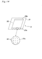
- dot-like spacers 60 may be formed on a surface of the first transparent electrode 12 of the first conductive panel 1 on the side for touch input or on a surface of the second transparent electrode 22 of the second conductive panel 2 on the screen side (see Fig. 14).
- transparent photo-setting resin such as acrylate resin including melamine acrylate resin, urethane acrylate resin, epoxy acrylate resin, methacrylacrylate resin, and acrylacrylate resin, and polyvinyl alcohol resin may be shaped into minute dots with photo process. A large number of minute dots as the spacers may be formed with printing process.
- dispersion of particles of inorganic substance or organic substance may be sprayed or applied and then dried.
- Dot-like spacers may be provided in the spaces (the cut-out sections 31) formed in the adhesive layer 3 cut from the outer edge side thereof or in the spaces (the punched hole sections 32) formed as holes punched in the adhesive layer 3.
- the spacers ensure insulation between the bus bar and the transparent electrode of the conductive panel on the opposite side in the spaces when input operations are not executed.
- the bus bar 23a is preferably covered with carbon layers 28.
- the cut-out sections 31 of the adhesive layer 3 open toward outside of the touch panel, and portions of the bus bar in the cut-out sections 31 that function as switches are accordingly exposed to outside air.
- Such covering with the carbon layers 28 can prevent oxidation of the bus bar 23a, without decreasing conductivity on a surface of the bus bar 23a.
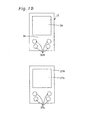
- Figs. 12A and 12B are the plan view and the exploded view showing the PDA (Personal Digital Assistants) as an example of a portable information device equipped with the wide range-inputable touch panel according to still another embodiment of the present invention.
- Fig. 13 is the exploded view showing the PDA equipped with the example of the conventional touch panel.
- reference character 70 denotes a housing of the PDA
- character 71 denotes a touch panel input section of the PDA that is an ordinary input section I
- character 72 denotes input buttons of the PDA that is an additional input section II
- character 74 denotes the touch panel of the PDA.
- a touch panel 90 having a configuration as shown in Fig. 11 and a membrane switch 91 are separately manufactured and are separately installed.
- the PDA equipped with the wide range-inputable touch panel according to still another embodiment of the present invention, shown in Figs. 12A and 12B, may be composed of one component as will be described below.
- first bus bars 13a and 13b of a first transparent electrode 12 on a first conductive panel 1 on a side for touch input are configured so as to be longer than second bus bars 23a and 23b of a second transparent electrode 22 on a second conductive panel 2 on a screen side, and a third input area 12B for the additional input section II other than a first input area 12A for the ordinary input section I is formed so as to have a large area.
- a second input area 22A of the second transparent electrode 22 is formed so as to be generally as large as the first input area 12A, and four circular additional electrode sections 23d, ..., 23d for a membrane switch substitutional switch section are formed and connected through extension line sections 23c to one of the second bus bars 23a on a second transparent insulating base 21 of the second conductive panel 2.
- the ordinary input section I may be composed of the first input area 12A of the first transparent electrode 12 and the second input area 22A of the second transparent electrode 22 that face each other through the region 3b of the adhesive layer 3 through which a screen of LCD or the like can be seen for input operations, as shown in Fig.
- Fig. 15 is an explanatory diagram of the adhesive layer 3 and an interconnection overcoating layer 27A of the PDA of Fig. 12B, through holes 3b and 27b are provided in regions of the layers that correspond to the second input area 22A of the second transparent electrode 22, and punched holes 32A, ..., 32A, and 27c, ..., 27c are provided in regions of the layers that correspond to the additional electrode sections 23d, ..., 23d.
- the third input area 12B of the first transparent electrode 12 for the membrane switch substitutional switch section is formed on the first transparent insulating base 11 of the first conductive panel 1 in the same manner as the first input area 12A of the first transparent electrode 12, and the additional electrode sections 23d, ..., 23d of the second transparent electrode 22 are formed on the second transparent insulating base 21 of the second conductive panel 2 in the same manner as the second input area 22A of the second transparent electrode 22.
- a membrane switch is incorporated into the touch panel, on the whole, and the PDA can be composed of one component.
- the third input area projecting out from between the first bus bars is formed in addition to the first input area between the first bus bars of the first transparent electrode, the first conductive panel and the second conductive panel are made to face each other and are stuck together in circumferential portions thereof with the insulating adhesive layer so that the first and second bus bars are rectangularly arranged, and the adhesive layer has the space sections that are arranged between at least one bus bar of the pair of second bus bars and the third input area of the first transparent electrode and that permit the bus bar and the third input area to be brought into electrical contact with each other by a press.
- the touch panel of analog resistance film type in which each of the conductive panels has the routing circuit connected to the bus bars is configured so that at least one bus bar and the transparent electrode on the conductive panel fronting the bus bar through the spaces formed in the adhesive layer cut out from the outer edge side thereof face each other so as to be capable of making electrical contact with each other by a press.
- the touch panel of analog resistance film type in which one conductive panel has the routing circuit connected to the bus bars on the panel and the routing circuit connected to the bus bars on the opposite panel is configured so that at least one bus bar on the conductive panel having the routing circuits collectively and the transparent electrode on the conductive panel fronting the bus bar through the spaces formed in the adhesive layer cut out from the outer edge side thereof face each other so as to be capable of making electrical contact with each other by a press.
- the third input area is added besides the first input area where the transparent electrodes face each other, a larger number of input operations may be made with one display operation on the screen, and input operations may be made over a wider area than in conventional configurations.
Landscapes
- Engineering & Computer Science (AREA)
- Theoretical Computer Science (AREA)
- General Engineering & Computer Science (AREA)
- Physics & Mathematics (AREA)
- General Physics & Mathematics (AREA)
- Human Computer Interaction (AREA)
- Artificial Intelligence (AREA)
- Computer Hardware Design (AREA)
- Computer Vision & Pattern Recognition (AREA)
- Position Input By Displaying (AREA)
- Push-Button Switches (AREA)
Abstract
Description
Claims (14)
- A wide range-inputable touch panel of analog resistance film type, the touch panel comprising:a first transparent insulating base (11);a pair of first bus bars (13a, 13b) arranged in parallel to each other on one surface of the first transparent insulating base (11);a first transparent electrode (12) having at least a first input area (12A) between the first bus bars;a second transparent insulating base (22);a pair of second bus bars (23a, 23b) arranged in parallel to each other on one surface of the second transparent insulating base (22); and .a second transparent electrode (22) having a second input area (22A) between the second bus bars that corresponds to the first input area (12A),the first transparent insulating base (11), the first bus bars (13a, 13b), and the first transparent electrode (12) composing a first conductive panel (1, 2), the second transparent insulating base (22), the second bus bars (23a, 23b), and the second transparent electrode (22) composing a second conductive panel (2),the first transparent electrode (12) further having a third input area (12B) that is adjacent to the first input area (12A) corresponding to the second input area (12B) and that corresponds to at least one bus bar of the pair of second bus bars,the touch panel further comprising:an insulating adhesive layer (3) that sticks together circumferential portions of the first and the second conductive panels (1, 2) facing each other so that the first and the second bus bars are arranged rectangularly and that has space sections (31, 31A, 32) provided between at least the one bus bar of the pair of second bus bars and the third input area (12B) of the first transparent electrode (12) and allowing the bus bar and the third input area to be brought into electrical contact with each other by a press; andfirst and second routing circuits (14a, 14b, 24a, 24b, 25a, 25b) connected respectively to the first and the second bus bars on the conductive panels.
- A wide range-inputable touch panel of analog resistance film type as claimed in claim 1, wherein the first and the second routing circuits (14a, 14b, 24a, 24b) are provided on the first and the second conductive panels, respectively, and are connected to the first and the second bus bars, respectively.
- A wide range-inputable touch panel of analog resistance film type as claimed in claim 1, wherein the first and the second routing circuits (24a, 24b, 25a, 25b) are provided on the second conductive panel and are connected to the first and the second bus bars, respectively.
- A wide range-inputable touch panel as claimed in any one of claims 1 through 3, wherein an insulating interconnection overcoating layer (27) is formed on a surface of the first conductive panel where the first routing circuit is formed or on a surface of the second conductive panel where the second routing circuit is formed, in an area that does not overlap portions of the bus bars on the surface which can be brought into electrical contact by a press with the facing transparent electrode and in an area including the routing circuit.
- A wide range-inputable touch panel of analog resistance film type as claimed in any one of claims 1 through 3, wherein the space sections are spaces (31, 31A) formed in the adhesive layer cut out from an outer edge side thereof.
- A wide range-inputable touch panel of analog resistance film type as claimed in claim 4, wherein the space sections are spaces (31, 31A) formed in the adhesive layer cut out from an outer edge side thereof.
- A wide range-inputable touch panel as claimed in any one of claims 1 through 3, wherein the space sections are spaces (31, 31A) in which two or more cut-out sections formed in the adhesive layer cut out from an outer edge side thereof exist side by side along one side.
- A wide range-inputable touch panel as claimed in claim 4, wherein the space sections are spaces (31, 31A) in which two or more cut-out sections formed in the adhesive layer cut out from an outer edge side thereof exist side by side along one side.
- A wide range-inputable touch panel as claimed in claim 7, wherein dot-like spacers (60) are provided in the spaces.
- A wide range-inputable touch panel as claimed in any one of claims 1 through 3, wherein at least the one bus bar of the pair of bus bars is covered with carbon layers (28) in cut-out sections of the adhesive layer.
- A wide range-inputable touch panel as claimed in any one of claims 1 through 3, wherein the space sections are punched holes (32) extending through the adhesive layer.
- A wide range-inputable touch panel as claimed in any one of claims 1 through 3, wherein the adhesive layer (3) has a through hole (3b) formed corresponding to the first input area (12A) of the first transparent electrode (12) and to the second input area (22A) of the second transparent electrode (22) and has a partition section (3c) that partitions the through hole (3b) and the space sections (31, 31A, 32).
- A wide range-inputable touch panel as claimed in any one of claims 1 through 3, wherein an ordinary input section (I) as a region through which a screen placed under the touch panel can be seen for input operations is composed of the first input area (12A) of the first transparent electrode (12) and of the second input area (22A) of the second transparent electrode (22) that faces the first input area (12A), and an additional input section (II) different from the ordinary input section (I) is composed of at least one bus bar of the pair of second bus bars and of the third input area (12B) of the first transparent electrode (12) that faces at least the one bus bar.
- A wide range-inputable touch panel as claimed in claim 13, wherein the additional input section (II) is composed of additional electrode sections (23d) that are connected through extension line sections (23c) to at least one bus bar (23a) of the pair of second bus bars, and the third input area (12B) of the first transparent electrode (12) that faces the additional electrode sections (23d) through the space sections.
Applications Claiming Priority (3)
| Application Number | Priority Date | Filing Date | Title |
|---|---|---|---|
| JP2000338028 | 2000-11-06 | ||
| JP2000338028 | 2000-11-06 | ||
| PCT/JP2001/009656 WO2002037253A1 (en) | 2000-11-06 | 2001-11-05 | Touch panel capable of wide-area inputting |
Publications (2)
| Publication Number | Publication Date |
|---|---|
| EP1333366A1 true EP1333366A1 (en) | 2003-08-06 |
| EP1333366A4 EP1333366A4 (en) | 2007-03-14 |
Family
ID=18813313
Family Applications (1)
| Application Number | Title | Priority Date | Filing Date |
|---|---|---|---|
| EP01979003A Withdrawn EP1333366A4 (en) | 2000-11-06 | 2001-11-05 | Touch panel capable of wide-area inputting |
Country Status (6)
| Country | Link |
|---|---|
| US (1) | US7071926B2 (en) |
| EP (1) | EP1333366A4 (en) |
| KR (1) | KR100816933B1 (en) |
| CN (1) | CN1318949C (en) |
| TW (1) | TW548627B (en) |
| WO (1) | WO2002037253A1 (en) |
Cited By (1)
| Publication number | Priority date | Publication date | Assignee | Title |
|---|---|---|---|---|
| RU2428746C1 (en) * | 2007-11-09 | 2011-09-10 | Моторола, Инк. | Mobile electronic device with capacitance sensor with restricted visibility isolation areas, and appropriate method |
Families Citing this family (31)
| Publication number | Priority date | Publication date | Assignee | Title |
|---|---|---|---|---|
| KR100875096B1 (en) * | 2002-08-02 | 2008-12-19 | 삼성모바일디스플레이주식회사 | Film printing apparatus used for manufacturing touch panel |
| US20040085299A1 (en) * | 2002-10-30 | 2004-05-06 | Jianming Huang | Combined touchscreen and membrane switch |
| TW555101U (en) * | 2002-11-25 | 2003-09-21 | Onetouch Technologies Co Ltd | Layout improvement of resistive lines of touch panel |
| CN100369052C (en) * | 2003-12-26 | 2008-02-13 | 无敌科技(西安)有限公司 | Customized input device and customized input method therefor |
| JP4424982B2 (en) * | 2003-12-26 | 2010-03-03 | 富士通コンポーネント株式会社 | Touch panel and manufacturing method thereof |
| US7382231B2 (en) * | 2004-02-12 | 2008-06-03 | Marjorie Blumberg | Electronic memory pad |
| US20100020045A1 (en) * | 2005-08-18 | 2010-01-28 | Kevin Walsh | Optically enhanced flat panel display system having integral touch screen |
| JP4285504B2 (en) * | 2006-05-24 | 2009-06-24 | ソニー株式会社 | Display device having touch panel |
| KR101385969B1 (en) * | 2007-03-21 | 2014-04-17 | 삼성전자주식회사 | Image forming apparatus |
| CN100582875C (en) * | 2007-04-13 | 2010-01-20 | 群康科技(深圳)有限公司 | Touch screen display apparatus |
| WO2009001946A1 (en) * | 2007-06-28 | 2008-12-31 | Kyocera Corporation | Touch panel, and touch panel type display device |
| KR100896775B1 (en) * | 2007-10-05 | 2009-05-11 | 에이디반도체(주) | Touch window with MID technology |
| US8199128B2 (en) * | 2008-05-29 | 2012-06-12 | Nissha Printing Co., Ltd. | Protection panel with touch input function |
| US20110012842A1 (en) * | 2008-09-26 | 2011-01-20 | Tovis Co., Ltd. | Touch panel using tempered glass |
| JP5331437B2 (en) * | 2008-10-09 | 2013-10-30 | 株式会社ジャパンディスプレイ | Liquid crystal display |
| KR101083071B1 (en) * | 2010-02-04 | 2011-11-16 | 주식회사 팬택 | Metal Dome Switch Integrated Touch Window of Mobile Device |
| US8531430B2 (en) * | 2010-02-11 | 2013-09-10 | Symbol Technologies, Inc. | Methods and apparatus for a touch panel display with integrated keys |
| CN102243544B (en) * | 2010-05-12 | 2013-08-14 | 群康科技(深圳)有限公司 | Touch screen, touch screen manufacturing method and touch display device |
| US8427817B2 (en) | 2010-10-15 | 2013-04-23 | Roche Diagnostics Operations, Inc. | Handheld diabetes manager with touch screen display |
| JP2012247895A (en) * | 2011-05-26 | 2012-12-13 | Alps Electric Co Ltd | Input device and manufacturing method of input device |
| MX353536B (en) * | 2011-06-10 | 2018-01-18 | Saint Gobain | Heatable composite pane having a security function. |
| KR20130000938A (en) * | 2011-06-24 | 2013-01-03 | 삼성디스플레이 주식회사 | Liquid crystal display device and method of manufacturing a liquid crystal display device |
| US20130082997A1 (en) * | 2011-09-30 | 2013-04-04 | Apple Inc. | System and method for detection of dimensions of display panel or other patterned device |
| KR20130037909A (en) * | 2011-10-07 | 2013-04-17 | 삼성전자주식회사 | Key input apparatus for portable terminal |
| KR102116469B1 (en) * | 2012-11-20 | 2020-05-29 | 삼성디스플레이 주식회사 | Display device with touch panel |
| CN104063075A (en) * | 2013-03-18 | 2014-09-24 | 林志忠 | Touch panel |
| TWI522241B (en) * | 2013-12-25 | 2016-02-21 | 恆顥科技股份有限公司 | Film for bonding to a substrate |
| JP2017097551A (en) * | 2015-11-20 | 2017-06-01 | 株式会社ジャパンディスプレイ | Display device and manufacturing method thereof |
| US10520780B2 (en) * | 2016-12-21 | 2019-12-31 | Southwall Technologies Inc. | Electroactive device provided with a trilayer bus bar |
| JP2018112937A (en) * | 2017-01-12 | 2018-07-19 | 株式会社ジャパンディスプレイ | Display device |
| CN108227989B (en) * | 2018-01-02 | 2021-03-05 | 京东方科技集团股份有限公司 | Touch substrate and preparation method thereof, metal mask plate and display device |
Family Cites Families (24)
| Publication number | Priority date | Publication date | Assignee | Title |
|---|---|---|---|---|
| JPS6033465Y2 (en) * | 1981-06-30 | 1985-10-05 | 日本電気ホームエレクトロニクス株式会社 | handwriting input device |
| JPS5916084A (en) * | 1982-07-19 | 1984-01-27 | Nitto Electric Ind Co Ltd | Input tablet |
| JPS6033465A (en) | 1983-08-04 | 1985-02-20 | 松下電器産業株式会社 | chemical heat pump |
| US4622437A (en) * | 1984-11-29 | 1986-11-11 | Interaction Systems, Inc. | Method and apparatus for improved electronic touch mapping |
| JPH0746309B2 (en) | 1986-07-31 | 1995-05-17 | 日本電気株式会社 | Data processing device |
| JPS6336430Y2 (en) * | 1987-06-15 | 1988-09-27 | ||
| JPH01147439A (en) | 1987-12-02 | 1989-06-09 | Asahi Optical Co Ltd | Automatic parallax correcting device for camera |
| JPH01147439U (en) * | 1988-03-31 | 1989-10-12 | ||
| JPH01281622A (en) * | 1988-05-09 | 1989-11-13 | Daicel Chem Ind Ltd | Transparent touch type input device |
| JPH0381815A (en) | 1989-08-25 | 1991-04-08 | Sharp Corp | Tablet input device |
| CA2082136C (en) * | 1991-11-08 | 1998-01-06 | Hiroshi Tsujioka | Coordinates input device |
| GB9507817D0 (en) * | 1995-04-18 | 1995-05-31 | Philips Electronics Uk Ltd | Touch sensing devices and methods of making such |
| JP3743458B2 (en) * | 1995-07-29 | 2006-02-08 | ソニー株式会社 | Input pad device |
| SE9504581L (en) * | 1995-12-21 | 1997-04-21 | Siemens Elema Ab | Device Panel |
| JPH1048625A (en) | 1996-08-02 | 1998-02-20 | Sumitomo Chem Co Ltd | Touch panel for liquid crystal display |
| JPH10260769A (en) | 1997-03-18 | 1998-09-29 | Fujitsu Takamizawa Component Kk | Coordinate input panel |
| JP3532378B2 (en) | 1997-04-08 | 2004-05-31 | 日本写真印刷株式会社 | Touch panel |
| TW388894B (en) * | 1997-10-09 | 2000-05-01 | Nissha Printing | High strength touch panel and manufacturing method therefor |
| JP3352972B2 (en) * | 1999-03-30 | 2002-12-03 | エスエムケイ株式会社 | Touch panel input device |
| DE60002464T2 (en) * | 1999-06-17 | 2004-03-18 | Nissha Printing Co., Ltd. | TOUCH-SENSITIVE PANEL WITH HIGH RELIABILITY |
| KR100745752B1 (en) * | 2005-06-28 | 2007-08-02 | 삼성전자주식회사 | Method for Purifying Carbonaceous Impurities in Carbon Nanotubes |
| JP3737101B1 (en) * | 2005-06-28 | 2006-01-18 | 株式会社サンヨープロジェクト | Exhaust gas purification device for internal combustion engine |
| JP4544059B2 (en) * | 2005-06-29 | 2010-09-15 | トヨタ紡織株式会社 | Goods storage box |
| JP4711122B2 (en) * | 2005-07-01 | 2011-06-29 | Dic株式会社 | Water absorbing material |
-
2001
- 2001-11-05 EP EP01979003A patent/EP1333366A4/en not_active Withdrawn
- 2001-11-05 TW TW090127424A patent/TW548627B/en not_active IP Right Cessation
- 2001-11-05 US US10/169,508 patent/US7071926B2/en not_active Expired - Fee Related
- 2001-11-05 WO PCT/JP2001/009656 patent/WO2002037253A1/en not_active Ceased
- 2001-11-05 CN CNB018034977A patent/CN1318949C/en not_active Expired - Fee Related
- 2001-11-05 KR KR1020027008741A patent/KR100816933B1/en not_active Expired - Fee Related
Cited By (1)
| Publication number | Priority date | Publication date | Assignee | Title |
|---|---|---|---|---|
| RU2428746C1 (en) * | 2007-11-09 | 2011-09-10 | Моторола, Инк. | Mobile electronic device with capacitance sensor with restricted visibility isolation areas, and appropriate method |
Also Published As
| Publication number | Publication date |
|---|---|
| EP1333366A4 (en) | 2007-03-14 |
| CN1394306A (en) | 2003-01-29 |
| WO2002037253A1 (en) | 2002-05-10 |
| US7071926B2 (en) | 2006-07-04 |
| KR100816933B1 (en) | 2008-03-26 |
| CN1318949C (en) | 2007-05-30 |
| TW548627B (en) | 2003-08-21 |
| US20030058225A1 (en) | 2003-03-27 |
| KR20020065639A (en) | 2002-08-13 |
Similar Documents
| Publication | Publication Date | Title |
|---|---|---|
| US7071926B2 (en) | Touch panel capable of wide-area inputting | |
| US6814452B2 (en) | Touch-panel with light shielding peripheral part | |
| JP4637294B2 (en) | Protective panel with touch input function | |
| JP4880723B2 (en) | Resistive touch panel with press detection function | |
| US20100053114A1 (en) | Touch panel apparatus and method for manufacturing the same | |
| WO2013035276A1 (en) | Integrated touch sensor substrate, display device provided with same, and method for producing integrated touch sensor substrate | |
| US8803830B2 (en) | Touch panel with conductive layers formed of parallel strips | |
| JP2008009921A (en) | Input device and its manufacturing method | |
| WO2010147045A1 (en) | Resistive film touch panel having a pressure-detecting function | |
| US7532131B2 (en) | Multi-layer solid state keyboard | |
| JP3764865B2 (en) | Touch panel capable of wide-area input | |
| JPH1195926A (en) | Touch panel | |
| JP2015064748A (en) | Integral type touch sensor substrate, display device including the same and manufacturing method of integral type touch sensor substrate | |
| KR101328763B1 (en) | Transparent circuit substrate for touchscreen and method for fabricating the same | |
| HK1056637A (en) | Touch panel capable of wide-area inputting | |
| JP2001216090A (en) | Narrow frame touch panel | |
| JP2010257986A (en) | Multi-layer solid state keyboard |
Legal Events
| Date | Code | Title | Description |
|---|---|---|---|
| PUAI | Public reference made under article 153(3) epc to a published international application that has entered the european phase |
Free format text: ORIGINAL CODE: 0009012 |
|
| 17P | Request for examination filed |
Effective date: 20030130 |
|
| AK | Designated contracting states |
Designated state(s): AT BE CH CY DE DK ES FI FR GB GR IE IT LI LU MC NL PT SE TR |
|
| A4 | Supplementary search report drawn up and despatched |
Effective date: 20070208 |
|
| 17Q | First examination report despatched |
Effective date: 20071219 |
|
| STAA | Information on the status of an ep patent application or granted ep patent |
Free format text: STATUS: THE APPLICATION HAS BEEN WITHDRAWN |
|
| 18W | Application withdrawn |
Effective date: 20111223 |
|
| REG | Reference to a national code |
Ref country code: HK Ref legal event code: WD Ref document number: 1056637 Country of ref document: HK |