EP1329953A1 - Carbon nanotube thermal interface structures - Google Patents
Carbon nanotube thermal interface structures Download PDFInfo
- Publication number
- EP1329953A1 EP1329953A1 EP02258760A EP02258760A EP1329953A1 EP 1329953 A1 EP1329953 A1 EP 1329953A1 EP 02258760 A EP02258760 A EP 02258760A EP 02258760 A EP02258760 A EP 02258760A EP 1329953 A1 EP1329953 A1 EP 1329953A1
- Authority
- EP
- European Patent Office
- Prior art keywords
- carbon nanotubes
- thermal interface
- array
- coupled
- thermally conductive
- Prior art date
- Legal status (The legal status is an assumption and is not a legal conclusion. Google has not performed a legal analysis and makes no representation as to the accuracy of the status listed.)
- Granted
Links
Images

Classifications
-
- H—ELECTRICITY
- H10—SEMICONDUCTOR DEVICES; ELECTRIC SOLID-STATE DEVICES NOT OTHERWISE PROVIDED FOR
- H10W—GENERIC PACKAGES, INTERCONNECTIONS, CONNECTORS OR OTHER CONSTRUCTIONAL DETAILS OF DEVICES COVERED BY CLASS H10
- H10W40/00—Arrangements for thermal protection or thermal control
- H10W40/20—Arrangements for cooling
- H10W40/25—Arrangements for cooling characterised by their materials
-
- B—PERFORMING OPERATIONS; TRANSPORTING
- B82—NANOTECHNOLOGY
- B82Y—SPECIFIC USES OR APPLICATIONS OF NANOSTRUCTURES; MEASUREMENT OR ANALYSIS OF NANOSTRUCTURES; MANUFACTURE OR TREATMENT OF NANOSTRUCTURES
- B82Y10/00—Nanotechnology for information processing, storage or transmission, e.g. quantum computing or single electron logic
-
- F—MECHANICAL ENGINEERING; LIGHTING; HEATING; WEAPONS; BLASTING
- F28—HEAT EXCHANGE IN GENERAL
- F28F—DETAILS OF HEAT-EXCHANGE AND HEAT-TRANSFER APPARATUS, OF GENERAL APPLICATION
- F28F13/00—Arrangements for modifying heat-transfer, e.g. increasing, decreasing
-
- F—MECHANICAL ENGINEERING; LIGHTING; HEATING; WEAPONS; BLASTING
- F28—HEAT EXCHANGE IN GENERAL
- F28F—DETAILS OF HEAT-EXCHANGE AND HEAT-TRANSFER APPARATUS, OF GENERAL APPLICATION
- F28F21/00—Constructions of heat-exchange apparatus characterised by the selection of particular materials
- F28F21/02—Constructions of heat-exchange apparatus characterised by the selection of particular materials of carbon, e.g. graphite
-
- H—ELECTRICITY
- H10—SEMICONDUCTOR DEVICES; ELECTRIC SOLID-STATE DEVICES NOT OTHERWISE PROVIDED FOR
- H10W—GENERIC PACKAGES, INTERCONNECTIONS, CONNECTORS OR OTHER CONSTRUCTIONAL DETAILS OF DEVICES COVERED BY CLASS H10
- H10W40/00—Arrangements for thermal protection or thermal control
- H10W40/20—Arrangements for cooling
- H10W40/25—Arrangements for cooling characterised by their materials
- H10W40/251—Organics
-
- H—ELECTRICITY
- H10—SEMICONDUCTOR DEVICES; ELECTRIC SOLID-STATE DEVICES NOT OTHERWISE PROVIDED FOR
- H10W—GENERIC PACKAGES, INTERCONNECTIONS, CONNECTORS OR OTHER CONSTRUCTIONAL DETAILS OF DEVICES COVERED BY CLASS H10
- H10W40/00—Arrangements for thermal protection or thermal control
- H10W40/70—Fillings or auxiliary members in containers or in encapsulations for thermal protection or control
- H10W40/77—Auxiliary members characterised by their shape
-
- F—MECHANICAL ENGINEERING; LIGHTING; HEATING; WEAPONS; BLASTING
- F28—HEAT EXCHANGE IN GENERAL
- F28F—DETAILS OF HEAT-EXCHANGE AND HEAT-TRANSFER APPARATUS, OF GENERAL APPLICATION
- F28F13/00—Arrangements for modifying heat-transfer, e.g. increasing, decreasing
- F28F2013/005—Thermal joints
- F28F2013/006—Heat conductive materials
-
- H—ELECTRICITY
- H10—SEMICONDUCTOR DEVICES; ELECTRIC SOLID-STATE DEVICES NOT OTHERWISE PROVIDED FOR
- H10W—GENERIC PACKAGES, INTERCONNECTIONS, CONNECTORS OR OTHER CONSTRUCTIONAL DETAILS OF DEVICES COVERED BY CLASS H10
- H10W72/00—Interconnections or connectors in packages
- H10W72/30—Die-attach connectors
- H10W72/321—Structures or relative sizes of die-attach connectors
- H10W72/325—Die-attach connectors having a filler embedded in a matrix
-
- H—ELECTRICITY
- H10—SEMICONDUCTOR DEVICES; ELECTRIC SOLID-STATE DEVICES NOT OTHERWISE PROVIDED FOR
- H10W—GENERIC PACKAGES, INTERCONNECTIONS, CONNECTORS OR OTHER CONSTRUCTIONAL DETAILS OF DEVICES COVERED BY CLASS H10
- H10W72/00—Interconnections or connectors in packages
- H10W72/30—Die-attach connectors
- H10W72/351—Materials of die-attach connectors
-
- H—ELECTRICITY
- H10—SEMICONDUCTOR DEVICES; ELECTRIC SOLID-STATE DEVICES NOT OTHERWISE PROVIDED FOR
- H10W—GENERIC PACKAGES, INTERCONNECTIONS, CONNECTORS OR OTHER CONSTRUCTIONAL DETAILS OF DEVICES COVERED BY CLASS H10
- H10W72/00—Interconnections or connectors in packages
- H10W72/30—Die-attach connectors
- H10W72/351—Materials of die-attach connectors
- H10W72/353—Materials of die-attach connectors not comprising solid metals or solid metalloids, e.g. ceramics
-
- H—ELECTRICITY
- H10—SEMICONDUCTOR DEVICES; ELECTRIC SOLID-STATE DEVICES NOT OTHERWISE PROVIDED FOR
- H10W—GENERIC PACKAGES, INTERCONNECTIONS, CONNECTORS OR OTHER CONSTRUCTIONAL DETAILS OF DEVICES COVERED BY CLASS H10
- H10W72/00—Interconnections or connectors in packages
- H10W72/30—Die-attach connectors
- H10W72/351—Materials of die-attach connectors
- H10W72/353—Materials of die-attach connectors not comprising solid metals or solid metalloids, e.g. ceramics
- H10W72/354—Materials of die-attach connectors not comprising solid metals or solid metalloids, e.g. ceramics comprising polymers
-
- H—ELECTRICITY
- H10—SEMICONDUCTOR DEVICES; ELECTRIC SOLID-STATE DEVICES NOT OTHERWISE PROVIDED FOR
- H10W—GENERIC PACKAGES, INTERCONNECTIONS, CONNECTORS OR OTHER CONSTRUCTIONAL DETAILS OF DEVICES COVERED BY CLASS H10
- H10W72/00—Interconnections or connectors in packages
- H10W72/851—Dispositions of multiple connectors or interconnections
- H10W72/874—On different surfaces
- H10W72/877—Bump connectors and die-attach connectors
-
- H—ELECTRICITY
- H10—SEMICONDUCTOR DEVICES; ELECTRIC SOLID-STATE DEVICES NOT OTHERWISE PROVIDED FOR
- H10W—GENERIC PACKAGES, INTERCONNECTIONS, CONNECTORS OR OTHER CONSTRUCTIONAL DETAILS OF DEVICES COVERED BY CLASS H10
- H10W90/00—Package configurations
- H10W90/701—Package configurations characterised by the relative positions of pads or connectors relative to package parts
- H10W90/731—Package configurations characterised by the relative positions of pads or connectors relative to package parts of die-attach connectors
- H10W90/736—Package configurations characterised by the relative positions of pads or connectors relative to package parts of die-attach connectors between a chip and a stacked lead frame, conducting package substrate or heat sink
-
- Y—GENERAL TAGGING OF NEW TECHNOLOGICAL DEVELOPMENTS; GENERAL TAGGING OF CROSS-SECTIONAL TECHNOLOGIES SPANNING OVER SEVERAL SECTIONS OF THE IPC; TECHNICAL SUBJECTS COVERED BY FORMER USPC CROSS-REFERENCE ART COLLECTIONS [XRACs] AND DIGESTS
- Y10—TECHNICAL SUBJECTS COVERED BY FORMER USPC
- Y10S—TECHNICAL SUBJECTS COVERED BY FORMER USPC CROSS-REFERENCE ART COLLECTIONS [XRACs] AND DIGESTS
- Y10S977/00—Nanotechnology
- Y10S977/70—Nanostructure
- Y10S977/832—Nanostructure having specified property, e.g. lattice-constant, thermal expansion coefficient
- Y10S977/833—Thermal property of nanomaterial, e.g. thermally conducting/insulating or exhibiting peltier or seebeck effect
Definitions
- the present invention relates generally to providing cooling solutions to electronic circuits, and, more specifically to the fabrication of a thermal interface structure using carbon nanotubes to improve thermal performance to a die containing an electronic circuit.
- the present invention relates to a thermal interface structure and method of forming it from a matrix of oriented carbon nanotubes projecting from a substrate.
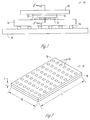
- FIG. 1 a portion of an electronic device such as a computer 10 is illustrated in an elevation view.
- a silicon die 12 which, in the embodiment shown, is mounted in a flip-chip ball grid array on an organic substrate 14 which is, in turn, mounted on a further substrate 16 and secured by solder balls 18.
- a cooling solution such as heat sink plate 20 is coupled to the surface of die 12 by a thermal interface structure 22 in the embodiment shown.
- thermal interface materials have been used in the past to reduce thermal resistance between a die and a cooling solution.
- thermal grease is used for the thermal interface material since such materials have high bulk thermal conductivity and readily conform to surface irregularities in the heat sink and the device.
- Use of thermal greases have the disadvantage of possible pump out and phase separation of the grease as the die is heated and undergoes thermal warping due to differences in the coefficient of thermal expansion between die 12 and organic substrate 14.
- adhesives such as epoxy are used as thermal interface material but have the disadvantage of requiring a cure process after their application.
- thermal gels such as silicones or certain olefins may also be used as thermal interface materials but they also require curing after application and have lower thermal conductivity than thermal grease.
- thermal interface materials have high bulk conductivity but suffer from high contact resistance and require that high pressure of at least 100 psi be applied at the thermal junction to provide adequate thermal coupling.
- phase change materials such as low molecular weight polyesters have been used but also suffer from the fact that their thermal conductivity is less than that of thermal grease.
- the thermal conductivity of thermal interface materials commonly used have a conductivity value of about 10 W/m-°K.
- a thermal interface structure is formed from an array of aligned carbon nanotubes in a polymeric interstitial material. Since the thermal conductivity of the carbon nanotubes is on the order of 3000 W/m-°K using them in a thermal interface structure will substantially increase its thermal conductivity.
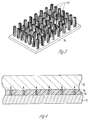
- a portion of a substrate 28 having an array of spaced bundles 24 of carbon nanotubes 26 projecting from the surface thereof is illustrated in highly enlarged form prior to injection of a polymer additive.
- Such arrays are available from Nano-Lab, Inc. which manufactures them under a chemical vapor deposition process described in an article of Dr. Z. F. Ren in Science, 282, 1105 (1998).
- the array of bundles 24 of nanotubes 26 which are produced in accordance with the process are grown on a variety of substrates 28 including glass and silicon.
- the nanotubes 26 grown on substrate 28 are aligned so that the majority of the nanotubes are oriented generally parallel to each other and perpendicular to the substrate 28 from which they project.
- the heights of the nanotubes are typically quite similar.
- a thermal interface structure 22 may be formed from a substrate 28 upon which nanotube bundles 26 are supported.
- a polymeric interstitial material 30 is injected around the nanotube bundles 26 to support the nanotubes.
- Suitable polymeric materials include polycarbonate, polypropylene and acetal. After addition of polymeric material 30, the substrate 28 upon which the nanotubes were originally formed is removed. Suitable processes -for removal of substrate 28 are mechanical grinding or chemical etching.
- the length L and width W of thermal interface structure 22 are selected to provide a substantial heat exchange surface while falling within the outlines of the exposed surface of die 12. In one embodiment the length and width are 2 cm and 1 cm.
- the maximum thickness t of the thermal interface structure is limited by the length of the carbon nanotubes but will typically fall within the range of about 5 to 20 microns.
- increasing the thickness of the thermal interface structure 22 will increase the thermal impedance of the path between the die and the heat sink.
- the carbon nanotubes are oriented generally parallel to each other and perpendicular to the top and bottom surfaces of structure 22, since they provide their greatest thermal conductivity along their longitudinal axes and it is desirable to have the conducted heat follow the shortest path between die 12 and heat sink 20.
- Figure 5 is a flow chart outlining an embodiment of the method of forming the thermal intermediate structure.
- an array 24 of nanotube bundles 26 includes a substrate 28 from which nanotubes 26 project.
- the array is embedded with an interstitial material 30 which is a polymeric material selected from the group consisting of polycarbonate, polypropylene, polyacetal, polyoxymethylene and polyformaldehyde.
- the interstitial material 30 is thermoplastic and is injected in molten form to embed it in the array to form an intermediate structure.
- any excess interstitial material 30 is removed from the intermediate and the substrate 28 upon which the nanotube bundles were originally grown.
- the removal can be performed by a chemical mechanical polishing process or by mechanical grinding.
- the thermal intermediate structure is completed.
- the carbon nanotubes remained aligned with each other throughout the forming of the structure and, after removal of excess interstitial material and the original substrate, the ends of the carbon nanotubes are at the surfaces of the thermal intermediate structure which engage the object to be cooled and the cooling solution surface to which the thermal intermediate structure couples it.
- the thermal intermediate structure provides thermal coupling between surfaces of two objects and the thermal intermediate structure is under pressure, yielding of the interstitial material will assure that the carbon nanotubes make secure thermal contacts with the surfaces of the objects which sandwich it, despite the presence of irregularities in the flatness of the surfaces.
- Figure 6 shows a process for providing a thermal coupling between two objects.
- a nanotube array is coupled to one of the objects.
- the nanotube array may actually be grown on the surface of the object rather than on a separate substrate.
- the injection with the interstitial material in operation 64 and the removal of the excess material are carried out in much the same manner of the operations shown in Figure 5.
- operation 62 is performed after the nanotubes are formed on a separate substrate and after the interstitial material has been applied in operation 64 and the excess material removed in operation 66.
- the operation 68 involves coupling the other surface of the array to the other of the two objects.
- one of the objects may be a cooling solution such as a heat sink and the other a semiconductor die.
- either of the objects can receive carbon nanotubes as they are grown in operation 62. Using that process, an additional advantage of a particularly strong thermal bond to that object is obtainable.
Landscapes
- Engineering & Computer Science (AREA)
- Physics & Mathematics (AREA)
- General Engineering & Computer Science (AREA)
- Chemical & Material Sciences (AREA)
- Nanotechnology (AREA)
- Thermal Sciences (AREA)
- Mechanical Engineering (AREA)
- Theoretical Computer Science (AREA)
- Crystallography & Structural Chemistry (AREA)
- Mathematical Physics (AREA)
- Cooling Or The Like Of Semiconductors Or Solid State Devices (AREA)
- Cooling Or The Like Of Electrical Apparatus (AREA)
- Carbon And Carbon Compounds (AREA)
Abstract
Description
- The present invention relates generally to providing cooling solutions to electronic circuits, and, more specifically to the fabrication of a thermal interface structure using carbon nanotubes to improve thermal performance to a die containing an electronic circuit.
- In order that the manner in which the embodiments of the invention are obtained, a more particular description of the invention briefly described above will be rendered by reference to specific embodiments thereof which are illustrated in the appended drawings. Understanding that these drawings depict only typical embodiments of the invention that are not necessarily drawn to scale and are not therefore to be considered to be limiting of its scope, the invention will be described and explained with additional specificity and detail through the use of the accompanying drawings in which:
- Figure 1 is an elevation view of a flip chip electronic device which is coupled to a cooling plate using a thermal interface according to an embodiment of the present invention;
- Figure 2 is a perspective view of a portion of the thermal interface of Figure 1, with polymer additive, showing carbon nanotube array bundles;
- Figure 3 is a perspective illustrational schematic view of a thermal interface showing, carbon nanotube bundles, in exaggerated scale distributed over the surface of the thermal interface;
- Figure 4 is an elevational cross-section of the thermal interface structure depicted in Figure 3 showing the flow of heat from the surface of the electronic device to the heat sink; and
- Figure 5 is a flow chart of a process for producing a thermal interface structure according to one embodiment of the present invention.
- Figure 6 is a flow chart of a process for providing a thermal path between two objects according to an embodiment of the present invention.
-
- The present invention relates to a thermal interface structure and method of forming it from a matrix of oriented carbon nanotubes projecting from a substrate.
- It will be readily understood to those skilled in the art that various other changes in the details, material, and arrangements of the parts and method stages which have been described and illustrated in order to explain the nature of this invention may be made without departing from the principles and scope of the invention as expressed in the claims.
- In Figure 1, a portion of an electronic device such as a
computer 10 is illustrated in an elevation view. Indevice 10, asilicon die 12 which, in the embodiment shown, is mounted in a flip-chip ball grid array on anorganic substrate 14 which is, in turn, mounted on afurther substrate 16 and secured bysolder balls 18. A cooling solution such asheat sink plate 20 is coupled to the surface of die 12 by athermal interface structure 22 in the embodiment shown. - A variety of thermal interface materials have been used in the past to reduce thermal resistance between a die and a cooling solution. In some applications, thermal grease is used for the thermal interface material since such materials have high bulk thermal conductivity and readily conform to surface irregularities in the heat sink and the device. Use of thermal greases, however, have the disadvantage of possible pump out and phase separation of the grease as the die is heated and undergoes thermal warping due to differences in the coefficient of thermal expansion between die 12 and
organic substrate 14. In other applications, adhesives such as epoxy are used as thermal interface material but have the disadvantage of requiring a cure process after their application. Various thermal gels such as silicones or certain olefins may also be used as thermal interface materials but they also require curing after application and have lower thermal conductivity than thermal grease. Certain elastomers such as urethane rubber have high bulk conductivity but suffer from high contact resistance and require that high pressure of at least 100 psi be applied at the thermal junction to provide adequate thermal coupling. Finally, certain phase change materials such as low molecular weight polyesters have been used but also suffer from the fact that their thermal conductivity is less than that of thermal grease. The thermal conductivity of thermal interface materials commonly used have a conductivity value of about 10 W/m-°K. - In one embodiment of the invention, a thermal interface structure is formed from an array of aligned carbon nanotubes in a polymeric interstitial material. Since the thermal conductivity of the carbon nanotubes is on the order of 3000 W/m-°K using them in a thermal interface structure will substantially increase its thermal conductivity.
- In Figure 2, a portion of a
substrate 28 having an array of spacedbundles 24 ofcarbon nanotubes 26 projecting from the surface thereof is illustrated in highly enlarged form prior to injection of a polymer additive. Such arrays are available from Nano-Lab, Inc. which manufactures them under a chemical vapor deposition process described in an article of Dr. Z. F. Ren in Science, 282, 1105 (1998). The array ofbundles 24 ofnanotubes 26 which are produced in accordance with the process are grown on a variety ofsubstrates 28 including glass and silicon. Thenanotubes 26 grown onsubstrate 28 are aligned so that the majority of the nanotubes are oriented generally parallel to each other and perpendicular to thesubstrate 28 from which they project. The heights of the nanotubes are typically quite similar. - A
thermal interface structure 22 may be formed from asubstrate 28 upon whichnanotube bundles 26 are supported. A polymericinterstitial material 30 is injected around thenanotube bundles 26 to support the nanotubes. Suitable polymeric materials include polycarbonate, polypropylene and acetal. After addition ofpolymeric material 30, thesubstrate 28 upon which the nanotubes were originally formed is removed. Suitable processes -for removal ofsubstrate 28 are mechanical grinding or chemical etching. - As shown in Figure 2, the length L and width W of
thermal interface structure 22 are selected to provide a substantial heat exchange surface while falling within the outlines of the exposed surface of die 12. In one embodiment the length and width are 2 cm and 1 cm. - The maximum thickness t of the thermal interface structure is limited by the length of the carbon nanotubes but will typically fall within the range of about 5 to 20 microns. Of course, increasing the thickness of the
thermal interface structure 22 will increase the thermal impedance of the path between the die and the heat sink. As shown in Figure 4, the carbon nanotubes are oriented generally parallel to each other and perpendicular to the top and bottom surfaces ofstructure 22, since they provide their greatest thermal conductivity along their longitudinal axes and it is desirable to have the conducted heat follow the shortest path between die 12 andheat sink 20. - Figure 5 is a flow chart outlining an embodiment of the method of forming the thermal intermediate structure. In
operation 52 anarray 24 ofnanotube bundles 26 includes asubstrate 28 from which nanotubes 26 project. The array is embedded with aninterstitial material 30 which is a polymeric material selected from the group consisting of polycarbonate, polypropylene, polyacetal, polyoxymethylene and polyformaldehyde. Theinterstitial material 30 is thermoplastic and is injected in molten form to embed it in the array to form an intermediate structure. - In
operation 54 any excessinterstitial material 30 is removed from the intermediate and thesubstrate 28 upon which the nanotube bundles were originally grown. The removal can be performed by a chemical mechanical polishing process or by mechanical grinding. At the conclusion ofoperation 54, the thermal intermediate structure is completed. The carbon nanotubes remained aligned with each other throughout the forming of the structure and, after removal of excess interstitial material and the original substrate, the ends of the carbon nanotubes are at the surfaces of the thermal intermediate structure which engage the object to be cooled and the cooling solution surface to which the thermal intermediate structure couples it. - If the thermal intermediate structure provides thermal coupling between surfaces of two objects and the thermal intermediate structure is under pressure, yielding of the interstitial material will assure that the carbon nanotubes make secure thermal contacts with the surfaces of the objects which sandwich it, despite the presence of irregularities in the flatness of the surfaces.
- Figure 6 shows a process for providing a thermal coupling between two objects. In
operation 62, a nanotube array is coupled to one of the objects. In one embodiment, the nanotube array may actually be grown on the surface of the object rather than on a separate substrate. In that embodiment it is necessary that the temperatures and other conditions under which the carbon nanotubes are formed by within the temperature ranges and exposure times permitted by the object upon which the nanotube array is grown. In this embodiment the injection with the interstitial material inoperation 64 and the removal of the excess material are carried out in much the same manner of the operations shown in Figure 5. - In another embodiment,
operation 62 is performed after the nanotubes are formed on a separate substrate and after the interstitial material has been applied inoperation 64 and the excess material removed inoperation 66. - In the embodiments the process shown in Figure 6 discussed above, the
operation 68 involves coupling the other surface of the array to the other of the two objects. In one embodiment one of the objects may be a cooling solution such as a heat sink and the other a semiconductor die. In one embodiment, either of the objects can receive carbon nanotubes as they are grown inoperation 62. Using that process, an additional advantage of a particularly strong thermal bond to that object is obtainable. - The foregoing description of the specific embodiments reveals the general nature of the invention sufficiently that others can, by applying current knowledge, readily modify and/or adapt it for various applications without departing from the generic concept and therefore such adaptations and modifications are intended to be comprehended within the meaning and range of equivalents of the disclosed embodiments.
- It is to be understood that the phraseology and terminology employed herein is for the purpose of description and not of limitation. Accordingly, the invention is intended to embrace all such alternatives, modifications, equivalents and variations as fall within the spirit and broad scope of the appended claims.
Claims (26)
- A thermal interface structure comprising:at least one carbon nanotube oriented substantially parallel to a desired heat transfer axis of the thermal interface; andan interstitial material in which the nanotubes are embedded.
- The structure of claim 1, wherein the structure has a first surface to contact a surface of a circuit die and a second surface to contact a surface of a cooling solution, the first and second surfaces being substantially parallel to each other.
- The structure of claim 2, wherein the thickness of the structure from the first surface to the second surface is about 5 to 20 microns.
- The structure of claim 1 wherein the interstitial material is a polymeric material.
- The structure of claim 4, wherein the polymeric material is selected from the group consisting of polycarbonate, polypropylene, polyacetal, polyoxymethylene and polyformaldehyde.
- A thermal interface comprising:at least one bundle of carbon nanotubes, the bundles oriented substantially parallel to each other and to a heat transfer flow path of the thermal interface; andan interstitial material between the bundles of nanotubes.
- The thermal interface of claim 6 wherein the interstitial material is a polymeric material.
- The thermal interface of claim 6 wherein the thermal interface has first and second generally planar surfaces which are each substantially perpendicular to the heat transfer path.
- A heat transfer structure for use with a semiconductor die comprising:a heat sink having a surface to couple to the die; anda thermally conductive element comprising a first surface coupled to the heat sink and a second surface coupled to the semiconductor die, the thermally conductive element comprising a plurality of carbon nanotubes oriented with their axes substantially perpendicular to the first and second surfaces.
- The heat transfer structure of claim 9 wherein the thermally conductive element also comprises an interstitial bonding material interspersed among the carbon nanotubes.
- The heat dissipating structure of claim 10 wherein the interstitial bonding material is a polymeric material selected from the group consisting of polycarbonate, polypropylene, polyacetal, polyoxymethylene and polyformaldehyde.
- The heat dissipating structure of claim 9 wherein the thermally conductive element has a surface area that is substantially the same as the surface area of the die.
- The heat dissipating structure of claim 12 wherein the thickness of the thermally conductive element is between 10 and 50 microns.
- An electronic assembly comprising at least one integrated circuit package comprising:at least one integrated circuit die;a heat sink having a surface coupled to the die; anda thermally conductive element comprising a first surface coupled to the heat sink and a second surface coupled to the die, the thermally conductive element comprising a plurality of carbon nanotubes oriented with their axes substantially perpendicular to the first and second surfaces.
- The electronic assembly of claim 14 wherein the thermally conductive element also comprises an interstitial material embedded among the carbon nanotubes.
- The electronic assembly of claim 15 wherein the interstitial material is a polymeric material selected from the group consisting of polycarbonate, polypropylene, polyacetal, polyoxymethylene and polyformaldehyde.
- A data processing system comprising:a bus coupling components to the data processing system;a display coupled to the bus;external memory coupled to the bus; anda processor coupled to the bus and comprising an electronic assembly including at least one electronic package comprising:at least one integrated circuit die;a heat sink having a surface coupled to the die; anda thermally conductive element comprising a first surface coupled to the heat sink and a second surface to couple to the die, the thermally conductive element comprising a plurality of carbon nanotubes oriented with their axes substantially perpendicular to the first and second surfaces.
- The data processing system of claim 17 wherein the thermally conductive element comprises an interstitial material interspersed among the carbon nanotubes.
- The data processing system of claim 18 wherein the interstitial material is a polymeric material selected from the group consisting of polycarbonate, polypropylene, polyacetal, polyoxymethylene and polyformaldehyde.
- A method of fabricating a thermal interface structure comprising:embedding an array of substantially aligned carbon nanotubes in an interstitial material to form an intermediate having a layer of substantially aligned carbon nanotubes embedded therein; andremoving excess material from the intermediate to provide a thermal interface structure having a first substantially planar surface for engaging a surface of one object and a second substantially planar surface for engaging a surface of another object, the first and second surfaces oriented substantially perpendicular to the substantially aligned carbon nanotubes.
- The method of claim 20 wherein the array of substantially aligned carbon nanotubes also comprises a substrate from which the carbon nanotubes project and wherein the removing of excess material also comprises removing at least a portion of the substrate.
- The method of claim 20 wherein removing excess material comprises chemical mechanical polishing of the intermediate.
- The method of claim 20 wherein removing excess material comprises etching the intermediate.
- A method of providing a thermal intermediate between two objects comprising:providing an array of substantially aligned carbon nanotubes coupled to one of the objects;embedding the array of substantially aligned carbon nanotubes in an interstitial material to form a layer of substantially aligned carbon nanotubes embedded therein; andcoupling the array to the other object.
- The method of claim 24 wherein providing the array coupled to the object comprises forming the carbon nanotubes on the surface of the object
- The method of claim 24 wherein providing the array coupled to the object comprisesforming the array on a substrate;embedding the array in an interstitial material;removing the substrate; andcoupling the array to the object.
Applications Claiming Priority (2)
| Application Number | Priority Date | Filing Date | Title |
|---|---|---|---|
| US10/027,442 US6965513B2 (en) | 2001-12-20 | 2001-12-20 | Carbon nanotube thermal interface structures |
| US27442 | 2001-12-20 |
Publications (2)
| Publication Number | Publication Date |
|---|---|
| EP1329953A1 true EP1329953A1 (en) | 2003-07-23 |
| EP1329953B1 EP1329953B1 (en) | 2014-01-22 |
Family
ID=21837757
Family Applications (1)
| Application Number | Title | Priority Date | Filing Date |
|---|---|---|---|
| EP02258760.4A Expired - Lifetime EP1329953B1 (en) | 2001-12-20 | 2002-12-19 | Carbon nanotube thermal interface structures |
Country Status (6)
| Country | Link |
|---|---|
| US (1) | US6965513B2 (en) |
| EP (1) | EP1329953B1 (en) |
| JP (1) | JP4541639B2 (en) |
| CN (1) | CN100576520C (en) |
| AU (1) | AU2002353167A1 (en) |
| WO (1) | WO2003054958A1 (en) |
Cited By (18)
| Publication number | Priority date | Publication date | Assignee | Title |
|---|---|---|---|---|
| WO2004114404A1 (en) * | 2003-06-17 | 2004-12-29 | Curamik Electronics Gmbh | Device comprising at least one heat source formed by a functional element that is to be cooled, at least one heat sink, and at least one intermediate layer located between the heat source and the heat sink and made of a thermally conducting material, and thermally conducting material, especially for use in such a device |
| US7094679B1 (en) | 2003-03-11 | 2006-08-22 | The United States Of America As Represented By The Administrator Of The National Aeronautics And Space Administration | Carbon nanotube interconnect |
| US7109581B2 (en) | 2003-08-25 | 2006-09-19 | Nanoconduction, Inc. | System and method using self-assembled nano structures in the design and fabrication of an integrated circuit micro-cooler |
| US7273095B2 (en) | 2003-03-11 | 2007-09-25 | United States Of America As Represented By The Administrator Of The National Aeronautics And Space Administration | Nanoengineered thermal materials based on carbon nanotube array composites |
| CN100364081C (en) * | 2003-11-08 | 2008-01-23 | 鸿富锦精密工业(深圳)有限公司 | Radiator and method of manufacturing the same |
| CN100404242C (en) * | 2005-04-14 | 2008-07-23 | 清华大学 | Thermal interface material and method of manufacturing the same |
| US7477527B2 (en) | 2005-03-21 | 2009-01-13 | Nanoconduction, Inc. | Apparatus for attaching a cooling structure to an integrated circuit |
| US7538422B2 (en) | 2003-08-25 | 2009-05-26 | Nanoconduction Inc. | Integrated circuit micro-cooler having multi-layers of tubes of a CNT array |
| US7656027B2 (en) | 2003-01-24 | 2010-02-02 | Nanoconduction, Inc. | In-chip structures and methods for removing heat from integrated circuits |
| US7678614B2 (en) | 2005-03-31 | 2010-03-16 | Tsinghua University | Thermal interface material and method for making the same |
| US7732918B2 (en) | 2003-08-25 | 2010-06-08 | Nanoconduction, Inc. | Vapor chamber heat sink having a carbon nanotube fluid interface |
| US8048688B2 (en) | 2006-10-24 | 2011-11-01 | Samsung Electronics Co., Ltd. | Method and apparatus for evaluation and improvement of mechanical and thermal properties of CNT/CNF arrays |
| US8093715B2 (en) | 2005-08-05 | 2012-01-10 | Purdue Research Foundation | Enhancement of thermal interface conductivities with carbon nanotube arrays |
| US8262835B2 (en) | 2007-12-19 | 2012-09-11 | Purdue Research Foundation | Method of bonding carbon nanotubes |
| CN1891780B (en) * | 2005-07-01 | 2013-04-24 | 清华大学 | Thermal interface material, and its preparing method |
| TWI452704B (en) * | 2009-12-17 | 2014-09-11 | Hon Hai Prec Ind Co Ltd | Solar energy generating device and solar energy generating module |
| EP2269948A4 (en) * | 2008-02-29 | 2015-08-05 | Fujitsu Ltd | SHEET STRUCTURE, SEMICONDUCTOR DEVICE, AND METHOD FOR GROWING CARBON STRUCTURE |
| US9346991B2 (en) | 2011-04-14 | 2016-05-24 | Ada Technologies, Inc. | Thermal interface materials and systems and devices containing the same |
Families Citing this family (174)
| Publication number | Priority date | Publication date | Assignee | Title |
|---|---|---|---|---|
| US7132161B2 (en) * | 1999-06-14 | 2006-11-07 | Energy Science Laboratories, Inc. | Fiber adhesive material |
| US20040009353A1 (en) * | 1999-06-14 | 2004-01-15 | Knowles Timothy R. | PCM/aligned fiber composite thermal interface |
| US6921462B2 (en) * | 2001-12-17 | 2005-07-26 | Intel Corporation | Method and apparatus for producing aligned carbon nanotube thermal interface structure |
| US8907323B2 (en) | 2002-04-23 | 2014-12-09 | Philip D. Freedman | Microprocessor assembly |
| US7800194B2 (en) * | 2002-04-23 | 2010-09-21 | Freedman Philip D | Thin film photodetector, method and system |
| US20070122622A1 (en) * | 2002-04-23 | 2007-05-31 | Freedman Philip D | Electronic module with thermal dissipating surface |
| US6856016B2 (en) * | 2002-07-02 | 2005-02-15 | Intel Corp | Method and apparatus using nanotubes for cooling and grounding die |
| US10340424B2 (en) | 2002-08-30 | 2019-07-02 | GE Lighting Solutions, LLC | Light emitting diode component |
| US6994584B1 (en) * | 2002-08-30 | 2006-02-07 | Advanced Micro Devices, Inc. | Thermally conductive integrated circuit mounting structures |
| US20050175769A1 (en) * | 2002-10-10 | 2005-08-11 | Tomoaki Kunugi | Heat transfer method and heat exchange system between solid and fluid |
| CN1296994C (en) * | 2002-11-14 | 2007-01-24 | 清华大学 | A thermal interfacial material and method for manufacturing same |
| TWI265541B (en) * | 2002-12-25 | 2006-11-01 | Hon Hai Prec Ind Co Ltd | Plasma display |
| US20040152240A1 (en) * | 2003-01-24 | 2004-08-05 | Carlos Dangelo | Method and apparatus for the use of self-assembled nanowires for the removal of heat from integrated circuits |
| US7316061B2 (en) | 2003-02-03 | 2008-01-08 | Intel Corporation | Packaging of integrated circuits with carbon nano-tube arrays to enhance heat dissipation through a thermal interface |
| DE10324377A1 (en) * | 2003-05-28 | 2005-01-05 | Infineon Technologies Ag | Heat extraction device has nanotube arrangement with nanotubes as material for heat extraction and embedded in embedding material, especially adhesive material |
| US7112472B2 (en) * | 2003-06-25 | 2006-09-26 | Intel Corporation | Methods of fabricating a composite carbon nanotube thermal interface device |
| US7481267B2 (en) * | 2003-06-26 | 2009-01-27 | The Regents Of The University Of California | Anisotropic thermal and electrical applications of composites of ceramics and carbon nanotubes |
| US6976532B2 (en) * | 2003-06-26 | 2005-12-20 | The Regents Of The University Of California | Anisotropic thermal applications of composites of ceramics and carbon nanotubes |
| US7168484B2 (en) * | 2003-06-30 | 2007-01-30 | Intel Corporation | Thermal interface apparatus, systems, and methods |
| US6864571B2 (en) * | 2003-07-07 | 2005-03-08 | Gelcore Llc | Electronic devices and methods for making same using nanotube regions to assist in thermal heat-sinking |
| WO2005052179A2 (en) * | 2003-08-13 | 2005-06-09 | The Johns Hopkins University | Method of making carbon nanotube arrays, and thermal interfaces using same |
| US8039961B2 (en) * | 2003-08-25 | 2011-10-18 | Samsung Electronics Co., Ltd. | Composite carbon nanotube-based structures and methods for removing heat from solid-state devices |
| US20070114658A1 (en) * | 2004-08-24 | 2007-05-24 | Carlos Dangelo | Integrated Circuit Micro-Cooler with Double-Sided Tubes of a CNT Array |
| US8080871B2 (en) * | 2003-08-25 | 2011-12-20 | Samsung Electronics Co., Ltd. | Carbon nanotube-based structures and methods for removing heat from solid-state devices |
| US20080131655A1 (en) * | 2006-03-21 | 2008-06-05 | Barbara Wacker | Double Layer Carbon Nanotube-Based Structures and Methods for Removing Heat from Solid-State Devices |
| US20070126116A1 (en) * | 2004-08-24 | 2007-06-07 | Carlos Dangelo | Integrated Circuit Micro-Cooler Having Tubes of a CNT Array in Essentially the Same Height over a Surface |
| US20080131722A1 (en) * | 2006-03-21 | 2008-06-05 | Ephraim Suhir | Single Layer Carbon Nanotube-Based Structures and Methods for Removing Heat from Solid-State Devices |
| KR100528925B1 (en) * | 2003-09-09 | 2005-11-15 | 삼성에스디아이 주식회사 | Heat dissipating sheet and plasma display device having the same |
| US20050126766A1 (en) * | 2003-09-16 | 2005-06-16 | Koila,Inc. | Nanostructure augmentation of surfaces for enhanced thermal transfer with improved contact |
| US20050129928A1 (en) * | 2003-09-16 | 2005-06-16 | Koila, Inc. | Nanostructure augmentation of surfaces for enhanced thermal transfer with increased surface area |
| US7235421B2 (en) * | 2003-09-16 | 2007-06-26 | Nasreen Chopra | System and method for developing production nano-material |
| TW200519346A (en) * | 2003-09-16 | 2005-06-16 | Koila Inc | Nanostructure augmentation of surfaces for enhanced thermal transfer |
| US20050116336A1 (en) * | 2003-09-16 | 2005-06-02 | Koila, Inc. | Nano-composite materials for thermal management applications |
| US20050089638A1 (en) * | 2003-09-16 | 2005-04-28 | Koila, Inc. | Nano-material thermal and electrical contact system |
| US20050214197A1 (en) * | 2003-09-17 | 2005-09-29 | Molecular Nanosystems, Inc. | Methods for producing and using catalytic substrates for carbon nanotube growth |
| WO2005025734A2 (en) * | 2003-09-17 | 2005-03-24 | Molecular Nanosystems, Inc. | Methods for producing and using catalytic substrates for carbon nanotube growth |
| DE10344492B4 (en) * | 2003-09-24 | 2006-09-07 | Carl Zeiss Nts Gmbh | Particle beam |
| DE10345157B4 (en) * | 2003-09-29 | 2009-01-08 | Qimonda Ag | Thermally conductive packaging of electronic circuit units |
| TW200517042A (en) * | 2003-11-04 | 2005-05-16 | Hon Hai Prec Ind Co Ltd | Heat sink |
| EP1697972A2 (en) * | 2003-11-18 | 2006-09-06 | Washington State University Research Foundation | Micro-transducer and thermal switch for same |
| CN100405587C (en) * | 2003-11-22 | 2008-07-23 | 鸿富锦精密工业(深圳)有限公司 | Radiator and its preparation method |
| US7180174B2 (en) * | 2003-12-30 | 2007-02-20 | Intel Corporation | Nanotube modified solder thermal intermediate structure, systems, and methods |
| US7456052B2 (en) * | 2003-12-30 | 2008-11-25 | Intel Corporation | Thermal intermediate apparatus, systems, and methods |
| US20050169831A1 (en) * | 2004-02-04 | 2005-08-04 | Montgomery Stephen W. | Three-dimensional nanotube structure |
| CN100383213C (en) * | 2004-04-02 | 2008-04-23 | 清华大学 | A kind of thermal interface material and its manufacturing method |
| CN1290764C (en) * | 2004-05-13 | 2006-12-20 | 清华大学 | Method for producing Nano carbon tubes in even length in large quantities |
| US20050255304A1 (en) * | 2004-05-14 | 2005-11-17 | Damon Brink | Aligned nanostructure thermal interface material |
| US20060025515A1 (en) * | 2004-07-27 | 2006-02-02 | Mainstream Engineering Corp. | Nanotube composites and methods for producing |
| US20060083927A1 (en) * | 2004-10-15 | 2006-04-20 | Zyvex Corporation | Thermal interface incorporating nanotubes |
| US20060090885A1 (en) * | 2004-10-29 | 2006-05-04 | Stephen Montgomery | Thermally conductive channel between a semiconductor chip and an external thermal interface |
| TWI388042B (en) * | 2004-11-04 | 2013-03-01 | 台灣積體電路製造股份有限公司 | Integrated circuit based on nanotube substrate |
| TW200633171A (en) * | 2004-11-04 | 2006-09-16 | Koninkl Philips Electronics Nv | Nanotube-based fluid interface material and approach |
| TWI247060B (en) * | 2004-12-31 | 2006-01-11 | Yonyu Plastics Co Ltd | Method producing vapor-grown carbon fibers having 3-d linkage structure |
| US7025607B1 (en) * | 2005-01-10 | 2006-04-11 | Endicott Interconnect Technologies, Inc. | Capacitor material with metal component for use in circuitized substrates, circuitized substrate utilizing same, method of making said circuitized substrate, and information handling system utilizing said circuitized substrate |
| CN100543103C (en) * | 2005-03-19 | 2009-09-23 | 清华大学 | Thermal interface material and preparation method thereof |
| US20060231237A1 (en) * | 2005-03-21 | 2006-10-19 | Carlos Dangelo | Apparatus and method for cooling ICs using nano-rod based chip-level heat sinks |
| CN100337981C (en) * | 2005-03-24 | 2007-09-19 | 清华大学 | Thermal interface material and its production method |
| CN1837147B (en) * | 2005-03-24 | 2010-05-05 | 清华大学 | Thermal interface material and preparation method thereof |
| US20060231946A1 (en) * | 2005-04-14 | 2006-10-19 | Molecular Nanosystems, Inc. | Nanotube surface coatings for improved wettability |
| CN100358132C (en) * | 2005-04-14 | 2007-12-26 | 清华大学 | Thermal interface material producing method |
| US7596751B2 (en) * | 2005-04-22 | 2009-09-29 | Hewlett-Packard Development Company, L.P. | Contact sheet based image management |
| KR101361946B1 (en) * | 2005-04-25 | 2014-02-12 | 스몰텍 에이비 | Controlled growth of a nanostructure on a substrate, and electron emission devices based on the same |
| US20060251897A1 (en) * | 2005-05-06 | 2006-11-09 | Molecular Nanosystems, Inc. | Growth of carbon nanotubes to join surfaces |
| AU2006249601B2 (en) * | 2005-05-26 | 2011-08-11 | Nanocomp Technologies, Inc. | Systems and methods for thermal management of electronic components |
| US7269008B2 (en) * | 2005-06-29 | 2007-09-11 | Intel Corporation | Cooling apparatus and method |
| KR100631993B1 (en) * | 2005-07-20 | 2006-10-09 | 삼성전기주식회사 | LED package and manufacturing method thereof |
| US7777291B2 (en) * | 2005-08-26 | 2010-08-17 | Smoltek Ab | Integrated circuits having interconnects and heat dissipators based on nanostructures |
| CN1929118B (en) * | 2005-09-05 | 2010-05-26 | 鸿富锦精密工业(深圳)有限公司 | Radiator and manufacturing method thereof |
| US20090048385A1 (en) * | 2005-09-16 | 2009-02-19 | Asahi Kasei Chemicals Corporation | Masterbatch and composition containing the same |
| US7297399B2 (en) * | 2005-10-11 | 2007-11-20 | General Electric Company | Thermal transport structure and associated method |
| US20080019097A1 (en) * | 2005-10-11 | 2008-01-24 | General Electric Company | Thermal transport structure |
| CN100517661C (en) * | 2005-11-26 | 2009-07-22 | 鸿富锦精密工业(深圳)有限公司 | Preparation method of heat radiator |
| US7871533B1 (en) * | 2006-01-12 | 2011-01-18 | South Dakota School Of Mines And Technology | Carbon nanoparticle-containing nanofluid |
| US20070158610A1 (en) * | 2006-01-12 | 2007-07-12 | Haiping Hong | Carbon naoparticle-containing hydrophilic nanofluid |
| US7494910B2 (en) * | 2006-03-06 | 2009-02-24 | Micron Technology, Inc. | Methods of forming semiconductor package |
| US7532475B2 (en) * | 2006-03-30 | 2009-05-12 | International Business Machines Corporation | Semiconductor chip assembly with flexible metal cantilevers |
| CN101054467B (en) * | 2006-04-14 | 2010-05-26 | 清华大学 | Carbon nanotube composite material and preparation method thereof |
| US7868531B2 (en) * | 2006-05-05 | 2011-01-11 | Brother International Corporation | Carbon nanotube arrays for field electron emission |
| US8890312B2 (en) * | 2006-05-26 | 2014-11-18 | The Hong Kong University Of Science And Technology | Heat dissipation structure with aligned carbon nanotube arrays and methods for manufacturing and use |
| JP4897360B2 (en) * | 2006-06-08 | 2012-03-14 | ポリマテック株式会社 | Thermally conductive molded body and method for producing the same |
| WO2008000045A1 (en) * | 2006-06-30 | 2008-01-03 | University Of Wollongong | Nanostructured composites |
| US20080026505A1 (en) * | 2006-07-28 | 2008-01-31 | Nirupama Chakrapani | Electronic packages with roughened wetting and non-wetting zones |
| US8389119B2 (en) * | 2006-07-31 | 2013-03-05 | The Board Of Trustees Of The Leland Stanford Junior University | Composite thermal interface material including aligned nanofiber with low melting temperature binder |
| CN100591613C (en) * | 2006-08-11 | 2010-02-24 | 清华大学 | Carbon nanotube composite material and manufacturing method thereof |
| US20080292835A1 (en) * | 2006-08-30 | 2008-11-27 | Lawrence Pan | Methods for forming freestanding nanotube objects and objects so formed |
| JP4917100B2 (en) * | 2006-09-22 | 2012-04-18 | インターナショナル・ビジネス・マシーンズ・コーポレーション | Method for manufacturing thermal interface structure |
| WO2008049015A2 (en) * | 2006-10-17 | 2008-04-24 | Purdue Research Foundation | Electrothermal interface material enhancer |
| US20100173228A1 (en) * | 2006-12-14 | 2010-07-08 | University Of Wollongong | Nanotube and Carbon Layer Nanostructured Composites |
| DE102007006175A1 (en) * | 2007-02-07 | 2008-08-14 | Osram Opto Semiconductors Gmbh | Heat conducting layer for use with optoelectronic arrangement, has two main surfaces and multiple heat conducting elements that are arranged on former main surface and has preferred directions, which cuts former main surface |
| JP4992461B2 (en) * | 2007-02-21 | 2012-08-08 | 富士通株式会社 | Electronic circuit device and electronic circuit device module |
| US8020621B2 (en) * | 2007-05-08 | 2011-09-20 | Baker Hughes Incorporated | Downhole applications of composites having aligned nanotubes for heat transport |
| US7743763B2 (en) * | 2007-07-27 | 2010-06-29 | The Boeing Company | Structurally isolated thermal interface |
| DE102007039905A1 (en) | 2007-08-23 | 2008-08-28 | Siemens Ag | Heat conducting material layer production method for use in solar technology, involves elongation of multiple nodular fibers in longitudinal direction having heat conductivity more than in another direction |
| DE102007039904A1 (en) | 2007-08-23 | 2008-08-28 | Siemens Ag | Heat-conductive material layer manufacturing method, involves inserting fibers in field area and transporting towards carrier layer, where fibers have large heat-conductivity toward fiber longitudinal direction than other direction |
| KR101487346B1 (en) * | 2007-09-12 | 2015-01-28 | 스몰텍 에이비 | Connecting and Bonding Adjacent Layers with Nanostructures |
| EP2190778A4 (en) * | 2007-09-28 | 2014-08-13 | Univ Brigham Young | CARBON NANOTUBES ASSEMBLY |
| US9305735B2 (en) | 2007-09-28 | 2016-04-05 | Brigham Young University | Reinforced polymer x-ray window |
| US8498381B2 (en) | 2010-10-07 | 2013-07-30 | Moxtek, Inc. | Polymer layer on X-ray window |
| US8919428B2 (en) * | 2007-10-17 | 2014-12-30 | Purdue Research Foundation | Methods for attaching carbon nanotubes to a carbon substrate |
| JP5252322B2 (en) * | 2007-10-17 | 2013-07-31 | エージェンシー フォー サイエンス, テクノロジー アンド リサーチ | Carbon nanotube and polymer-containing composite film |
| JP5104688B2 (en) * | 2007-10-22 | 2012-12-19 | 富士通株式会社 | Sheet-like structure, method for producing the same, and electronic device |
| JP5018419B2 (en) * | 2007-11-19 | 2012-09-05 | 富士通株式会社 | Module structure, manufacturing method thereof, and semiconductor device |
| JP5746808B2 (en) * | 2007-11-22 | 2015-07-08 | 富士通株式会社 | Package and electronic device using carbon nanotube |
| US7760507B2 (en) * | 2007-12-26 | 2010-07-20 | The Bergquist Company | Thermally and electrically conductive interconnect structures |
| CN102007571B (en) | 2008-02-25 | 2016-01-20 | 斯莫特克有限公司 | Deposition and selective removal of conductive helplayers during nanostructure fabrication |
| JP5146256B2 (en) * | 2008-03-18 | 2013-02-20 | 富士通株式会社 | Sheet-like structure and manufacturing method thereof, and electronic device and manufacturing method thereof |
| US20090323276A1 (en) * | 2008-06-25 | 2009-12-31 | Mongia Rajiv K | High performance spreader for lid cooling applications |
| CN101626674B (en) * | 2008-07-11 | 2015-07-01 | 清华大学 | Radiating structure and preparation method thereof |
| EP2330077A4 (en) * | 2008-09-18 | 2015-08-05 | Nitto Denko Corp | Carbon nanotube aggregate |
| JP2010073842A (en) * | 2008-09-18 | 2010-04-02 | Nitto Denko Corp | Microprocessor structure |
| JP2010073843A (en) * | 2008-09-18 | 2010-04-02 | Nitto Denko Corp | Microprocessor structure |
| KR100978571B1 (en) * | 2008-10-27 | 2010-08-27 | 삼성엘이디 주식회사 | LED Package |
| JP5239768B2 (en) * | 2008-11-14 | 2013-07-17 | 富士通株式会社 | Heat dissipating material, electronic equipment and manufacturing method thereof |
| US20100128439A1 (en) * | 2008-11-24 | 2010-05-27 | General Electric Company | Thermal management system with graphene-based thermal interface material |
| CN101768427B (en) * | 2009-01-07 | 2012-06-20 | 清华大学 | Thermal interface material and preparation method thereof |
| US20100190023A1 (en) * | 2009-01-26 | 2010-07-29 | Adam Franklin Gross | Metal bonded nanotube array |
| KR20100087932A (en) * | 2009-01-29 | 2010-08-06 | 삼성전기주식회사 | A method for die attach using self-assemble monolayer and a package substrate attached die using the self-assemble monolayer |
| CN101814867B (en) * | 2009-02-20 | 2013-03-20 | 清华大学 | Thermoelectric generator |
| TWI473309B (en) * | 2009-02-27 | 2015-02-11 | 鴻海精密工業股份有限公司 | Thermoelectric generator |
| CN101826467B (en) * | 2009-03-02 | 2012-01-25 | 清华大学 | Preparation method of thermal interface material |
| US8541058B2 (en) * | 2009-03-06 | 2013-09-24 | Timothy S. Fisher | Palladium thiolate bonding of carbon nanotubes |
| US8247971B1 (en) | 2009-03-19 | 2012-08-21 | Moxtek, Inc. | Resistively heated small planar filament |
| JP5431793B2 (en) * | 2009-05-29 | 2014-03-05 | 新光電気工業株式会社 | Heat dissipation component, electronic component device, and method of manufacturing electronic component device |
| JP5605360B2 (en) * | 2009-06-16 | 2014-10-15 | 富士通株式会社 | Graphite structure, electronic component, and method of manufacturing electronic component |
| US8405996B2 (en) * | 2009-06-30 | 2013-03-26 | General Electric Company | Article including thermal interface element and method of preparation |
| US8593040B2 (en) | 2009-10-02 | 2013-11-26 | Ge Lighting Solutions Llc | LED lamp with surface area enhancing fins |
| CA2786838C (en) * | 2010-01-14 | 2017-01-10 | Saab Ab | Multifunctional de-icing/anti-icing system |
| US8662452B2 (en) * | 2010-01-14 | 2014-03-04 | Saab Ab | Article with de-icing/anti-icing function |
| US10240772B2 (en) * | 2010-04-02 | 2019-03-26 | GE Lighting Solutions, LLC | Lightweight heat sinks and LED lamps employing same |
| US8668356B2 (en) * | 2010-04-02 | 2014-03-11 | GE Lighting Solutions, LLC | Lightweight heat sinks and LED lamps employing same |
| JP2013524439A (en) * | 2010-04-02 | 2013-06-17 | ジーイー ライティング ソリューションズ エルエルシー | Light weight heat sink and LED lamp using the same |
| US8564954B2 (en) | 2010-06-15 | 2013-10-22 | Chipmos Technologies Inc. | Thermally enhanced electronic package |
| US9096784B2 (en) | 2010-07-23 | 2015-08-04 | International Business Machines Corporation | Method and system for allignment of graphite nanofibers for enhanced thermal interface material performance |
| JP5373731B2 (en) * | 2010-10-05 | 2013-12-18 | トヨタ自動車株式会社 | Method for producing catalyst carrier |
| US10962297B2 (en) | 2011-02-21 | 2021-03-30 | Board Of Regents, The University Of Texas System | Multidimensional heat transfer system for cooling electronic components |
| US8989354B2 (en) | 2011-05-16 | 2015-03-24 | Brigham Young University | Carbon composite support structure |
| US9174412B2 (en) | 2011-05-16 | 2015-11-03 | Brigham Young University | High strength carbon fiber composite wafers for microfabrication |
| US9076628B2 (en) | 2011-05-16 | 2015-07-07 | Brigham Young University | Variable radius taper x-ray window support structure |
| US9257359B2 (en) * | 2011-07-22 | 2016-02-09 | International Business Machines Corporation | System and method to process horizontally aligned graphite nanofibers in a thermal interface material used in 3D chip stacks |
| US9874688B2 (en) | 2012-04-26 | 2018-01-23 | Acacia Communications, Inc. | Co-packaging photonic integrated circuits and application specific integrated circuits |
| US9500355B2 (en) | 2012-05-04 | 2016-11-22 | GE Lighting Solutions, LLC | Lamp with light emitting elements surrounding active cooling device |
| US9656246B2 (en) | 2012-07-11 | 2017-05-23 | Carbice Corporation | Vertically aligned arrays of carbon nanotubes formed on multilayer substrates |
| CN102840488A (en) * | 2012-09-11 | 2012-12-26 | 广东宏泰照明科技有限公司 | LED lights with cooling function |
| US9111899B2 (en) | 2012-09-13 | 2015-08-18 | Lenovo | Horizontally and vertically aligned graphite nanofibers thermal interface material for use in chip stacks |
| US9245813B2 (en) | 2013-01-30 | 2016-01-26 | International Business Machines Corporation | Horizontally aligned graphite nanofibers in etched silicon wafer troughs for enhanced thermal performance |
| US9090004B2 (en) | 2013-02-06 | 2015-07-28 | International Business Machines Corporation | Composites comprised of aligned carbon fibers in chain-aligned polymer binder |
| US9173623B2 (en) | 2013-04-19 | 2015-11-03 | Samuel Soonho Lee | X-ray tube and receiver inside mouth |
| US9082744B2 (en) | 2013-07-08 | 2015-07-14 | International Business Machines Corporation | Method for aligning carbon nanotubes containing magnetic nanoparticles in a thermosetting polymer using a magnetic field |
| JP5864486B2 (en) * | 2013-07-24 | 2016-02-17 | 富士通株式会社 | Sheet-like structure and method for producing the same |
| CN104349648B (en) * | 2013-08-09 | 2017-03-01 | 技嘉科技股份有限公司 | Composite cooling components |
| WO2015191897A1 (en) | 2014-06-11 | 2015-12-17 | Georgia Tech Research Corporation | Polymer-based nanostructured materials with tunable properties and methods of making thereof |
| US20160106005A1 (en) * | 2014-10-13 | 2016-04-14 | Ntherma Corporation | Carbon nanotubes as a thermal interface material |
| SG10201805058VA (en) | 2014-10-29 | 2018-07-30 | Acacia Communications Inc | Optoelectronic ball grid array package with fiber |
| US10444515B2 (en) | 2015-01-20 | 2019-10-15 | Microsoft Technology Licensing, Llc | Convective optical mount structure |
| US9791704B2 (en) | 2015-01-20 | 2017-10-17 | Microsoft Technology Licensing, Llc | Bonded multi-layer graphite heat pipe |
| US10028418B2 (en) | 2015-01-20 | 2018-07-17 | Microsoft Technology Licensing, Llc | Metal encased graphite layer heat pipe |
| US10108017B2 (en) | 2015-01-20 | 2018-10-23 | Microsoft Technology Licensing, Llc | Carbon nanoparticle infused optical mount |
| US20160286692A1 (en) * | 2015-03-23 | 2016-09-29 | The Boeing Company | High thermal conductivity joint utlizing continuous aligned carbon nanotubes |
| CN105128372B (en) * | 2015-09-22 | 2017-04-19 | 清华大学 | Preparation method for composite polymer film with high thermal conductivity |
| US10292255B2 (en) | 2016-05-18 | 2019-05-14 | Raytheon Company | Expanding thermal device and system for effecting heat transfer within electronics assemblies |
| US10791651B2 (en) | 2016-05-31 | 2020-09-29 | Carbice Corporation | Carbon nanotube-based thermal interface materials and methods of making and using thereof |
| US10153224B2 (en) | 2016-09-14 | 2018-12-11 | Globalfoundries Inc. | Backside spacer structures for improved thermal performance |
| TWI755492B (en) | 2017-03-06 | 2022-02-21 | 美商卡爾拜斯有限公司 | Carbon nanotube-based thermal interface materials and methods of making and using thereof |
| DE102017126028B4 (en) | 2017-06-30 | 2020-12-10 | Taiwan Semiconductor Manufacturing Co., Ltd. | Housing and manufacturing method using a release film as an insulating film |
| US10170341B1 (en) * | 2017-06-30 | 2019-01-01 | Taiwan Semiconductor Manufacturing Company, Ltd. | Release film as isolation film in package |
| DE102017217105A1 (en) * | 2017-09-26 | 2019-03-28 | Robert Bosch Gmbh | Cooling device and method for cooling an element to be cooled |
| CN108306075B (en) * | 2018-01-31 | 2019-11-08 | 陈攀攀 | A kind of thick variable section heat pipe cooling device of power battery monomer stacked module |
| US10707596B2 (en) | 2018-09-21 | 2020-07-07 | Carbice Corporation | Coated electrical connectors and methods of making and using thereof |
| CN111417282B (en) * | 2019-01-04 | 2021-07-30 | 清华大学 | Heat sink and electronic device using the heat sink |
| USD903610S1 (en) | 2019-08-28 | 2020-12-01 | Carbice Corporation | Flexible heat sink |
| USD906269S1 (en) | 2019-08-28 | 2020-12-29 | Carbice Corporation | Flexible heat sink |
| USD904322S1 (en) | 2019-08-28 | 2020-12-08 | Carbice Corporation | Flexible heat sink |
| US20210063099A1 (en) | 2019-08-28 | 2021-03-04 | Carbice Corporation | Flexible and conformable polymer-based heat sinks and methods of making and using thereof |
| US20230105760A1 (en) * | 2020-03-27 | 2023-04-06 | Tomoegawa Co., Ltd. | Metal fiber molded body, temperature regulation unit, and method for manufacturing metal fiber molded body |
Citations (8)
| Publication number | Priority date | Publication date | Assignee | Title |
|---|---|---|---|---|
| US5965267A (en) | 1995-02-17 | 1999-10-12 | Arizona Board Of Regents On Behalf Of The University Of Arizona | Method for producing encapsulated nanoparticles and carbon nanotubes using catalytic disproportionation of carbon monoxide and the nanoencapsulates and nanotubes formed thereby |
| WO1999067811A2 (en) | 1998-06-24 | 1999-12-29 | Johnson Matthey Electronics, Inc. | Electronic device having fibrous interface |
| WO2000033628A1 (en) * | 1998-12-02 | 2000-06-08 | Intel Corporation | A fibrous thermal interface adaptor |
| EP1054036A1 (en) * | 1999-05-18 | 2000-11-22 | Fina Research S.A. | Reinforced polymers |
| WO2001030694A1 (en) | 1999-10-27 | 2001-05-03 | William Marsh Rice University | Macroscopic ordered assembly of carbon nanotubes |
| EP1109218A2 (en) * | 1999-12-17 | 2001-06-20 | Polymatech Co., Ltd. | Heat conducting mold and manufacturing method thereof |
| WO2001092381A1 (en) | 1999-12-07 | 2001-12-06 | William Marsh Rice University | Oriented nanofibers embedded in polymer matrix |
| US6407922B1 (en) * | 2000-09-29 | 2002-06-18 | Intel Corporation | Heat spreader, electronic package including the heat spreader, and methods of manufacturing the heat spreader |
Family Cites Families (9)
| Publication number | Priority date | Publication date | Assignee | Title |
|---|---|---|---|---|
| US6203814B1 (en) | 1994-12-08 | 2001-03-20 | Hyperion Catalysis International, Inc. | Method of making functionalized nanotubes |
| US5753088A (en) | 1997-02-18 | 1998-05-19 | General Motors Corporation | Method for making carbon nanotubes |
| US6006168A (en) * | 1997-12-12 | 1999-12-21 | Digital Equipment Corporation | Thermal model for central processing unit |
| US6232706B1 (en) | 1998-11-12 | 2001-05-15 | The Board Of Trustees Of The Leland Stanford Junior University | Self-oriented bundles of carbon nanotubes and method of making same |
| US6331209B1 (en) * | 1999-04-21 | 2001-12-18 | Jin Jang | Method of forming carbon nanotubes |
| US6256996B1 (en) | 1999-12-09 | 2001-07-10 | International Business Machines Corporation | Nanoscopic thermoelectric coolers |
| JP2002121404A (en) * | 2000-10-19 | 2002-04-23 | Polymatech Co Ltd | Thermal conductive polymer sheet |
| JP4697829B2 (en) * | 2001-03-15 | 2011-06-08 | ポリマテック株式会社 | Carbon nanotube composite molded body and method for producing the same |
| US6667548B2 (en) * | 2001-04-06 | 2003-12-23 | Intel Corporation | Diamond heat spreading and cooling technique for integrated circuits |
-
2001
- 2001-12-20 US US10/027,442 patent/US6965513B2/en not_active Expired - Lifetime
-
2002
- 2002-12-17 WO PCT/US2002/040515 patent/WO2003054958A1/en not_active Ceased
- 2002-12-17 CN CN02828255A patent/CN100576520C/en not_active Expired - Fee Related
- 2002-12-17 AU AU2002353167A patent/AU2002353167A1/en not_active Abandoned
- 2002-12-18 JP JP2002366897A patent/JP4541639B2/en not_active Expired - Fee Related
- 2002-12-19 EP EP02258760.4A patent/EP1329953B1/en not_active Expired - Lifetime
Patent Citations (8)
| Publication number | Priority date | Publication date | Assignee | Title |
|---|---|---|---|---|
| US5965267A (en) | 1995-02-17 | 1999-10-12 | Arizona Board Of Regents On Behalf Of The University Of Arizona | Method for producing encapsulated nanoparticles and carbon nanotubes using catalytic disproportionation of carbon monoxide and the nanoencapsulates and nanotubes formed thereby |
| WO1999067811A2 (en) | 1998-06-24 | 1999-12-29 | Johnson Matthey Electronics, Inc. | Electronic device having fibrous interface |
| WO2000033628A1 (en) * | 1998-12-02 | 2000-06-08 | Intel Corporation | A fibrous thermal interface adaptor |
| EP1054036A1 (en) * | 1999-05-18 | 2000-11-22 | Fina Research S.A. | Reinforced polymers |
| WO2001030694A1 (en) | 1999-10-27 | 2001-05-03 | William Marsh Rice University | Macroscopic ordered assembly of carbon nanotubes |
| WO2001092381A1 (en) | 1999-12-07 | 2001-12-06 | William Marsh Rice University | Oriented nanofibers embedded in polymer matrix |
| EP1109218A2 (en) * | 1999-12-17 | 2001-06-20 | Polymatech Co., Ltd. | Heat conducting mold and manufacturing method thereof |
| US6407922B1 (en) * | 2000-09-29 | 2002-06-18 | Intel Corporation | Heat spreader, electronic package including the heat spreader, and methods of manufacturing the heat spreader |
Non-Patent Citations (1)
| Title |
|---|
| ANDREWS R ET AL: "NANOTUBE COMPOSITE CARBON FIBERS", APPLIED PHYSICS LETTERS, AMERICAN INSTITUTE OF PHYSICS. NEW YORK, US, VOL. 75, NR. 9, PAGE(S) 1329-1331, ISSN: 0003-6951, XP000868231 * |
Cited By (23)
| Publication number | Priority date | Publication date | Assignee | Title |
|---|---|---|---|---|
| US7656027B2 (en) | 2003-01-24 | 2010-02-02 | Nanoconduction, Inc. | In-chip structures and methods for removing heat from integrated circuits |
| US7217650B1 (en) | 2003-03-11 | 2007-05-15 | The United States Of America As Represented By The Administrator Of The National Aeronautics And Space Administration (Nasa) | Metallic nanowire interconnections for integrated circuit fabrication |
| US7273095B2 (en) | 2003-03-11 | 2007-09-25 | United States Of America As Represented By The Administrator Of The National Aeronautics And Space Administration | Nanoengineered thermal materials based on carbon nanotube array composites |
| US7094679B1 (en) | 2003-03-11 | 2006-08-22 | The United States Of America As Represented By The Administrator Of The National Aeronautics And Space Administration | Carbon nanotube interconnect |
| US7800908B2 (en) | 2003-06-17 | 2010-09-21 | Curamik Electronics Gmbh | Device with a heat source formed by a function element that is to be cooled, at least one heat sink, and at least one intermediate layer located between the heat source and the heat sink |
| WO2004114404A1 (en) * | 2003-06-17 | 2004-12-29 | Curamik Electronics Gmbh | Device comprising at least one heat source formed by a functional element that is to be cooled, at least one heat sink, and at least one intermediate layer located between the heat source and the heat sink and made of a thermally conducting material, and thermally conducting material, especially for use in such a device |
| US7109581B2 (en) | 2003-08-25 | 2006-09-19 | Nanoconduction, Inc. | System and method using self-assembled nano structures in the design and fabrication of an integrated circuit micro-cooler |
| US8039953B2 (en) | 2003-08-25 | 2011-10-18 | Samsung Electronics Co., Ltd. | System and method using self-assembled nano structures in the design and fabrication of an integrated circuit micro-cooler |
| US7538422B2 (en) | 2003-08-25 | 2009-05-26 | Nanoconduction Inc. | Integrated circuit micro-cooler having multi-layers of tubes of a CNT array |
| US7732918B2 (en) | 2003-08-25 | 2010-06-08 | Nanoconduction, Inc. | Vapor chamber heat sink having a carbon nanotube fluid interface |
| CN100364081C (en) * | 2003-11-08 | 2008-01-23 | 鸿富锦精密工业(深圳)有限公司 | Radiator and method of manufacturing the same |
| US7784531B1 (en) | 2004-04-13 | 2010-08-31 | The United States Of America As Represented By The Administrator Of The National Aeronautics And Space Administration | Nanoengineered thermal materials based on carbon nanotube array composites |
| US7477527B2 (en) | 2005-03-21 | 2009-01-13 | Nanoconduction, Inc. | Apparatus for attaching a cooling structure to an integrated circuit |
| US7678614B2 (en) | 2005-03-31 | 2010-03-16 | Tsinghua University | Thermal interface material and method for making the same |
| CN100404242C (en) * | 2005-04-14 | 2008-07-23 | 清华大学 | Thermal interface material and method of manufacturing the same |
| CN1891780B (en) * | 2005-07-01 | 2013-04-24 | 清华大学 | Thermal interface material, and its preparing method |
| US8093715B2 (en) | 2005-08-05 | 2012-01-10 | Purdue Research Foundation | Enhancement of thermal interface conductivities with carbon nanotube arrays |
| US8048688B2 (en) | 2006-10-24 | 2011-11-01 | Samsung Electronics Co., Ltd. | Method and apparatus for evaluation and improvement of mechanical and thermal properties of CNT/CNF arrays |
| US8262835B2 (en) | 2007-12-19 | 2012-09-11 | Purdue Research Foundation | Method of bonding carbon nanotubes |
| US8419885B2 (en) | 2007-12-19 | 2013-04-16 | Purdue Research Foundation | Method of bonding carbon nanotubes |
| EP2269948A4 (en) * | 2008-02-29 | 2015-08-05 | Fujitsu Ltd | SHEET STRUCTURE, SEMICONDUCTOR DEVICE, AND METHOD FOR GROWING CARBON STRUCTURE |
| TWI452704B (en) * | 2009-12-17 | 2014-09-11 | Hon Hai Prec Ind Co Ltd | Solar energy generating device and solar energy generating module |
| US9346991B2 (en) | 2011-04-14 | 2016-05-24 | Ada Technologies, Inc. | Thermal interface materials and systems and devices containing the same |
Also Published As
| Publication number | Publication date |
|---|---|
| US6965513B2 (en) | 2005-11-15 |
| CN1623230A (en) | 2005-06-01 |
| AU2002353167A1 (en) | 2003-07-09 |
| EP1329953B1 (en) | 2014-01-22 |
| CN100576520C (en) | 2009-12-30 |
| WO2003054958A1 (en) | 2003-07-03 |
| US20030117770A1 (en) | 2003-06-26 |
| JP4541639B2 (en) | 2010-09-08 |
| JP2003249613A (en) | 2003-09-05 |
Similar Documents
| Publication | Publication Date | Title |
|---|---|---|
| EP1329953B1 (en) | Carbon nanotube thermal interface structures | |
| US12183659B2 (en) | Embedded cooling assemblies for advanced device packaging and methods of manufacturing the same | |
| US6800945B2 (en) | Multi-chip semiconductor device with specific chip arrangement | |
| KR101387706B1 (en) | Semiconductor Package, Method of Fabricating the Same and Electronic Device Including the Same | |
| US20100172101A1 (en) | Thermal interface material and method for manufacturing the same | |
| TWI521614B (en) | Drop mold integration material as a package for an integrated circuit package system | |
| US8304293B2 (en) | Thermally enhanced semiconductor package | |
| US9892994B2 (en) | Graphene based filler material of superior thermal conductivity for chip attachment in microstructure devices | |
| TWI564974B (en) | Semiconductor device and method of packaging the same | |
| US20050179126A1 (en) | Diamond-silicon hybrid integrated heat spreader | |
| JPH09129791A (en) | Substrate-mounted heat sink and thermal connection structure for multiple integrated circuits | |
| US20160322277A1 (en) | Integration of backside heat spreader for thermal management | |
| TW201526177A (en) | Method for reducing warpage of circuit structure | |
| JP6261352B2 (en) | Carbon nanotube sheet, semiconductor device, method of manufacturing carbon nanotube sheet, and method of manufacturing semiconductor device | |
| US6566748B1 (en) | Flip-chip semiconductor device having an improved reliability | |
| US7679145B2 (en) | Transistor performance enhancement using engineered strains | |
| EP3751603B1 (en) | Semiconductor package with a heat sink bonded to a semiconductor chip with a bonding layer and to a molding material with a thermal interface material | |
| US20130032270A1 (en) | Thermal compression bonding with separate bond heads | |
| US7166540B2 (en) | Method for reducing assembly-induced stress in a semiconductor die | |
| US20040145047A1 (en) | Cooling micro-channels | |
| CN113345855B (en) | Thermal management materials for semiconductor devices and associated systems and methods | |
| US20030171006A1 (en) | Apparatus and methods for enhancing thermal performance of integrated circuit packages | |
| US6555413B1 (en) | Method for interconnecting semiconductor elements to form a thermoelectric cooler and a thermoelectric cooler formed therefrom | |
| Chen et al. | Multichip thin-film technology for low temperature packaging (CCD image sensors) | |
| KR100836769B1 (en) | Semiconductor chip package and method for manufacturing semiconductor package including same |
Legal Events
| Date | Code | Title | Description |
|---|---|---|---|
| PUAI | Public reference made under article 153(3) epc to a published international application that has entered the european phase |
Free format text: ORIGINAL CODE: 0009012 |
|
| AK | Designated contracting states |
Designated state(s): AT BE BG CH CY CZ DE DK EE ES FI FR GB GR IE IT LI LU MC NL PT SE SI SK TR |
|
| AX | Request for extension of the european patent |
Extension state: AL LT LV MK RO |
|
| 17P | Request for examination filed |
Effective date: 20040119 |
|
| AKX | Designation fees paid |
Designated state(s): AT BE BG CH CY CZ DE DK EE ES FI FR GB GR IE IT LI LU MC NL PT SE SI SK TR |
|
| 17Q | First examination report despatched |
Effective date: 20081110 |
|
| GRAP | Despatch of communication of intention to grant a patent |
Free format text: ORIGINAL CODE: EPIDOSNIGR1 |
|
| RIC1 | Information provided on ipc code assigned before grant |
Ipc: F28F 21/02 20060101ALI20130730BHEP Ipc: F28F 21/00 20060101ALI20130730BHEP Ipc: H01L 23/433 20060101AFI20130730BHEP Ipc: F28F 13/00 20060101ALI20130730BHEP Ipc: H01L 23/373 20060101ALI20130730BHEP Ipc: B82Y 10/00 20110101ALI20130730BHEP |
|
| INTG | Intention to grant announced |
Effective date: 20130822 |
|
| GRAS | Grant fee paid |
Free format text: ORIGINAL CODE: EPIDOSNIGR3 |
|
| GRAA | (expected) grant |
Free format text: ORIGINAL CODE: 0009210 |
|
| AK | Designated contracting states |
Kind code of ref document: B1 Designated state(s): AT BE BG CH CY CZ DE DK EE ES FI FR GB GR IE IT LI LU MC NL PT SE SI SK TR |
|
| REG | Reference to a national code |
Ref country code: GB Ref legal event code: FG4D |
|
| REG | Reference to a national code |
Ref country code: CH Ref legal event code: EP |
|
| REG | Reference to a national code |
Ref country code: AT Ref legal event code: REF Ref document number: 651130 Country of ref document: AT Kind code of ref document: T Effective date: 20140215 |
|
| REG | Reference to a national code |
Ref country code: IE Ref legal event code: FG4D |
|
| REG | Reference to a national code |
Ref country code: DE Ref legal event code: R096 Ref document number: 60245955 Country of ref document: DE Effective date: 20140306 |
|
| REG | Reference to a national code |
Ref country code: NL Ref legal event code: T3 |
|
| REG | Reference to a national code |
Ref country code: AT Ref legal event code: MK05 Ref document number: 651130 Country of ref document: AT Kind code of ref document: T Effective date: 20140122 |
|
| PG25 | Lapsed in a contracting state [announced via postgrant information from national office to epo] |
Ref country code: PT Free format text: LAPSE BECAUSE OF FAILURE TO SUBMIT A TRANSLATION OF THE DESCRIPTION OR TO PAY THE FEE WITHIN THE PRESCRIBED TIME-LIMIT Effective date: 20140522 Ref country code: AT Free format text: LAPSE BECAUSE OF FAILURE TO SUBMIT A TRANSLATION OF THE DESCRIPTION OR TO PAY THE FEE WITHIN THE PRESCRIBED TIME-LIMIT Effective date: 20140122 Ref country code: SE Free format text: LAPSE BECAUSE OF FAILURE TO SUBMIT A TRANSLATION OF THE DESCRIPTION OR TO PAY THE FEE WITHIN THE PRESCRIBED TIME-LIMIT Effective date: 20140122 Ref country code: CY Free format text: LAPSE BECAUSE OF FAILURE TO SUBMIT A TRANSLATION OF THE DESCRIPTION OR TO PAY THE FEE WITHIN THE PRESCRIBED TIME-LIMIT Effective date: 20140122 Ref country code: ES Free format text: LAPSE BECAUSE OF FAILURE TO SUBMIT A TRANSLATION OF THE DESCRIPTION OR TO PAY THE FEE WITHIN THE PRESCRIBED TIME-LIMIT Effective date: 20140122 Ref country code: FI Free format text: LAPSE BECAUSE OF FAILURE TO SUBMIT A TRANSLATION OF THE DESCRIPTION OR TO PAY THE FEE WITHIN THE PRESCRIBED TIME-LIMIT Effective date: 20140122 |
|
| PG25 | Lapsed in a contracting state [announced via postgrant information from national office to epo] |
Ref country code: BE Free format text: LAPSE BECAUSE OF FAILURE TO SUBMIT A TRANSLATION OF THE DESCRIPTION OR TO PAY THE FEE WITHIN THE PRESCRIBED TIME-LIMIT Effective date: 20140122 |
|
| REG | Reference to a national code |
Ref country code: DE Ref legal event code: R097 Ref document number: 60245955 Country of ref document: DE |
|
| PG25 | Lapsed in a contracting state [announced via postgrant information from national office to epo] |
Ref country code: DK Free format text: LAPSE BECAUSE OF FAILURE TO SUBMIT A TRANSLATION OF THE DESCRIPTION OR TO PAY THE FEE WITHIN THE PRESCRIBED TIME-LIMIT Effective date: 20140122 Ref country code: CZ Free format text: LAPSE BECAUSE OF FAILURE TO SUBMIT A TRANSLATION OF THE DESCRIPTION OR TO PAY THE FEE WITHIN THE PRESCRIBED TIME-LIMIT Effective date: 20140122 Ref country code: EE Free format text: LAPSE BECAUSE OF FAILURE TO SUBMIT A TRANSLATION OF THE DESCRIPTION OR TO PAY THE FEE WITHIN THE PRESCRIBED TIME-LIMIT Effective date: 20140122 |
|
| PG25 | Lapsed in a contracting state [announced via postgrant information from national office to epo] |
Ref country code: SK Free format text: LAPSE BECAUSE OF FAILURE TO SUBMIT A TRANSLATION OF THE DESCRIPTION OR TO PAY THE FEE WITHIN THE PRESCRIBED TIME-LIMIT Effective date: 20140122 |
|
| PLBE | No opposition filed within time limit |
Free format text: ORIGINAL CODE: 0009261 |
|
| STAA | Information on the status of an ep patent application or granted ep patent |
Free format text: STATUS: NO OPPOSITION FILED WITHIN TIME LIMIT |
|
| 26N | No opposition filed |
Effective date: 20141023 |
|
| REG | Reference to a national code |
Ref country code: DE Ref legal event code: R097 Ref document number: 60245955 Country of ref document: DE Effective date: 20141023 |
|
| PG25 | Lapsed in a contracting state [announced via postgrant information from national office to epo] |
Ref country code: SI Free format text: LAPSE BECAUSE OF FAILURE TO SUBMIT A TRANSLATION OF THE DESCRIPTION OR TO PAY THE FEE WITHIN THE PRESCRIBED TIME-LIMIT Effective date: 20140122 |
|
| PG25 | Lapsed in a contracting state [announced via postgrant information from national office to epo] |
Ref country code: LU Free format text: LAPSE BECAUSE OF FAILURE TO SUBMIT A TRANSLATION OF THE DESCRIPTION OR TO PAY THE FEE WITHIN THE PRESCRIBED TIME-LIMIT Effective date: 20141219 |
|
| REG | Reference to a national code |
Ref country code: CH Ref legal event code: PL |
|
| REG | Reference to a national code |
Ref country code: IE Ref legal event code: MM4A |
|
| REG | Reference to a national code |
Ref country code: FR Ref legal event code: ST Effective date: 20150831 |
|
| PG25 | Lapsed in a contracting state [announced via postgrant information from national office to epo] |
Ref country code: IE Free format text: LAPSE BECAUSE OF NON-PAYMENT OF DUE FEES Effective date: 20141219 Ref country code: CH Free format text: LAPSE BECAUSE OF NON-PAYMENT OF DUE FEES Effective date: 20141231 Ref country code: LI Free format text: LAPSE BECAUSE OF NON-PAYMENT OF DUE FEES Effective date: 20141231 |
|
| PG25 | Lapsed in a contracting state [announced via postgrant information from national office to epo] |
Ref country code: FR Free format text: LAPSE BECAUSE OF NON-PAYMENT OF DUE FEES Effective date: 20141231 |
|
| PG25 | Lapsed in a contracting state [announced via postgrant information from national office to epo] |
Ref country code: BG Free format text: LAPSE BECAUSE OF FAILURE TO SUBMIT A TRANSLATION OF THE DESCRIPTION OR TO PAY THE FEE WITHIN THE PRESCRIBED TIME-LIMIT Effective date: 20140122 Ref country code: MC Free format text: LAPSE BECAUSE OF FAILURE TO SUBMIT A TRANSLATION OF THE DESCRIPTION OR TO PAY THE FEE WITHIN THE PRESCRIBED TIME-LIMIT Effective date: 20140122 |
|
| PG25 | Lapsed in a contracting state [announced via postgrant information from national office to epo] |
Ref country code: IT Free format text: LAPSE BECAUSE OF FAILURE TO SUBMIT A TRANSLATION OF THE DESCRIPTION OR TO PAY THE FEE WITHIN THE PRESCRIBED TIME-LIMIT Effective date: 20140122 Ref country code: GR Free format text: LAPSE BECAUSE OF FAILURE TO SUBMIT A TRANSLATION OF THE DESCRIPTION OR TO PAY THE FEE WITHIN THE PRESCRIBED TIME-LIMIT Effective date: 20140423 |
|
| PG25 | Lapsed in a contracting state [announced via postgrant information from national office to epo] |
Ref country code: TR Free format text: LAPSE BECAUSE OF FAILURE TO SUBMIT A TRANSLATION OF THE DESCRIPTION OR TO PAY THE FEE WITHIN THE PRESCRIBED TIME-LIMIT Effective date: 20140122 |
|
| PGFP | Annual fee paid to national office [announced via postgrant information from national office to epo] |
Ref country code: DE Payment date: 20181204 Year of fee payment: 17 Ref country code: NL Payment date: 20181213 Year of fee payment: 17 |
|
| PGFP | Annual fee paid to national office [announced via postgrant information from national office to epo] |
Ref country code: GB Payment date: 20181219 Year of fee payment: 17 |
|
| REG | Reference to a national code |
Ref country code: DE Ref legal event code: R119 Ref document number: 60245955 Country of ref document: DE |
|
| REG | Reference to a national code |
Ref country code: NL Ref legal event code: MM Effective date: 20200101 |
|
| GBPC | Gb: european patent ceased through non-payment of renewal fee |
Effective date: 20191219 |
|
| PG25 | Lapsed in a contracting state [announced via postgrant information from national office to epo] |
Ref country code: NL Free format text: LAPSE BECAUSE OF NON-PAYMENT OF DUE FEES Effective date: 20200101 |
|
| PG25 | Lapsed in a contracting state [announced via postgrant information from national office to epo] |
Ref country code: DE Free format text: LAPSE BECAUSE OF NON-PAYMENT OF DUE FEES Effective date: 20200701 Ref country code: GB Free format text: LAPSE BECAUSE OF NON-PAYMENT OF DUE FEES Effective date: 20191219 |