US8080871B2 - Carbon nanotube-based structures and methods for removing heat from solid-state devices - Google Patents
Carbon nanotube-based structures and methods for removing heat from solid-state devices Download PDFInfo
- Publication number
- US8080871B2 US8080871B2 US12/177,815 US17781508A US8080871B2 US 8080871 B2 US8080871 B2 US 8080871B2 US 17781508 A US17781508 A US 17781508A US 8080871 B2 US8080871 B2 US 8080871B2
- Authority
- US
- United States
- Prior art keywords
- interface material
- thermal interface
- carbon nanotubes
- solid
- thermal
- Prior art date
- Legal status (The legal status is an assumption and is not a legal conclusion. Google has not performed a legal analysis and makes no representation as to the accuracy of the status listed.)
- Active, expires
Links
Images


Classifications
-
- H—ELECTRICITY
- H01—ELECTRIC ELEMENTS
- H01L—SEMICONDUCTOR DEVICES NOT COVERED BY CLASS H10
- H01L23/00—Details of semiconductor or other solid state devices
- H01L23/34—Arrangements for cooling, heating, ventilating or temperature compensation ; Temperature sensing arrangements
- H01L23/36—Selection of materials, or shaping, to facilitate cooling or heating, e.g. heatsinks
- H01L23/373—Cooling facilitated by selection of materials for the device or materials for thermal expansion adaptation, e.g. carbon
-
- B—PERFORMING OPERATIONS; TRANSPORTING
- B82—NANOTECHNOLOGY
- B82Y—SPECIFIC USES OR APPLICATIONS OF NANOSTRUCTURES; MEASUREMENT OR ANALYSIS OF NANOSTRUCTURES; MANUFACTURE OR TREATMENT OF NANOSTRUCTURES
- B82Y10/00—Nanotechnology for information processing, storage or transmission, e.g. quantum computing or single electron logic
-
- H—ELECTRICITY
- H01—ELECTRIC ELEMENTS
- H01L—SEMICONDUCTOR DEVICES NOT COVERED BY CLASS H10
- H01L23/00—Details of semiconductor or other solid state devices
- H01L23/34—Arrangements for cooling, heating, ventilating or temperature compensation ; Temperature sensing arrangements
- H01L23/46—Arrangements for cooling, heating, ventilating or temperature compensation ; Temperature sensing arrangements involving the transfer of heat by flowing fluids
- H01L23/473—Arrangements for cooling, heating, ventilating or temperature compensation ; Temperature sensing arrangements involving the transfer of heat by flowing fluids by flowing liquids
-
- H—ELECTRICITY
- H01—ELECTRIC ELEMENTS
- H01L—SEMICONDUCTOR DEVICES NOT COVERED BY CLASS H10
- H01L25/00—Assemblies consisting of a plurality of individual semiconductor or other solid state devices ; Multistep manufacturing processes thereof
- H01L25/03—Assemblies consisting of a plurality of individual semiconductor or other solid state devices ; Multistep manufacturing processes thereof all the devices being of a type provided for in the same subgroup of groups H01L27/00 - H01L33/00, or in a single subclass of H10K, H10N, e.g. assemblies of rectifier diodes
- H01L25/04—Assemblies consisting of a plurality of individual semiconductor or other solid state devices ; Multistep manufacturing processes thereof all the devices being of a type provided for in the same subgroup of groups H01L27/00 - H01L33/00, or in a single subclass of H10K, H10N, e.g. assemblies of rectifier diodes the devices not having separate containers
- H01L25/065—Assemblies consisting of a plurality of individual semiconductor or other solid state devices ; Multistep manufacturing processes thereof all the devices being of a type provided for in the same subgroup of groups H01L27/00 - H01L33/00, or in a single subclass of H10K, H10N, e.g. assemblies of rectifier diodes the devices not having separate containers the devices being of a type provided for in group H01L27/00
- H01L25/0652—Assemblies consisting of a plurality of individual semiconductor or other solid state devices ; Multistep manufacturing processes thereof all the devices being of a type provided for in the same subgroup of groups H01L27/00 - H01L33/00, or in a single subclass of H10K, H10N, e.g. assemblies of rectifier diodes the devices not having separate containers the devices being of a type provided for in group H01L27/00 the devices being arranged next and on each other, i.e. mixed assemblies
-
- H—ELECTRICITY
- H01—ELECTRIC ELEMENTS
- H01L—SEMICONDUCTOR DEVICES NOT COVERED BY CLASS H10
- H01L2224/00—Indexing scheme for arrangements for connecting or disconnecting semiconductor or solid-state bodies and methods related thereto as covered by H01L24/00
- H01L2224/01—Means for bonding being attached to, or being formed on, the surface to be connected, e.g. chip-to-package, die-attach, "first-level" interconnects; Manufacturing methods related thereto
- H01L2224/42—Wire connectors; Manufacturing methods related thereto
- H01L2224/44—Structure, shape, material or disposition of the wire connectors prior to the connecting process
- H01L2224/45—Structure, shape, material or disposition of the wire connectors prior to the connecting process of an individual wire connector
- H01L2224/45001—Core members of the connector
- H01L2224/4501—Shape
- H01L2224/45012—Cross-sectional shape
- H01L2224/45015—Cross-sectional shape being circular
-
- H—ELECTRICITY
- H01—ELECTRIC ELEMENTS
- H01L—SEMICONDUCTOR DEVICES NOT COVERED BY CLASS H10
- H01L2224/00—Indexing scheme for arrangements for connecting or disconnecting semiconductor or solid-state bodies and methods related thereto as covered by H01L24/00
- H01L2224/01—Means for bonding being attached to, or being formed on, the surface to be connected, e.g. chip-to-package, die-attach, "first-level" interconnects; Manufacturing methods related thereto
- H01L2224/42—Wire connectors; Manufacturing methods related thereto
- H01L2224/44—Structure, shape, material or disposition of the wire connectors prior to the connecting process
- H01L2224/45—Structure, shape, material or disposition of the wire connectors prior to the connecting process of an individual wire connector
- H01L2224/45001—Core members of the connector
- H01L2224/45099—Material
- H01L2224/451—Material with a principal constituent of the material being a metal or a metalloid, e.g. boron (B), silicon (Si), germanium (Ge), arsenic (As), antimony (Sb), tellurium (Te) and polonium (Po), and alloys thereof
- H01L2224/45138—Material with a principal constituent of the material being a metal or a metalloid, e.g. boron (B), silicon (Si), germanium (Ge), arsenic (As), antimony (Sb), tellurium (Te) and polonium (Po), and alloys thereof the principal constituent melting at a temperature of greater than or equal to 950°C and less than 1550°C
- H01L2224/45147—Copper (Cu) as principal constituent
-
- H—ELECTRICITY
- H01—ELECTRIC ELEMENTS
- H01L—SEMICONDUCTOR DEVICES NOT COVERED BY CLASS H10
- H01L2924/00—Indexing scheme for arrangements or methods for connecting or disconnecting semiconductor or solid-state bodies as covered by H01L24/00
- H01L2924/0001—Technical content checked by a classifier
- H01L2924/00014—Technical content checked by a classifier the subject-matter covered by the group, the symbol of which is combined with the symbol of this group, being disclosed without further technical details
-
- Y—GENERAL TAGGING OF NEW TECHNOLOGICAL DEVELOPMENTS; GENERAL TAGGING OF CROSS-SECTIONAL TECHNOLOGIES SPANNING OVER SEVERAL SECTIONS OF THE IPC; TECHNICAL SUBJECTS COVERED BY FORMER USPC CROSS-REFERENCE ART COLLECTIONS [XRACs] AND DIGESTS
- Y10—TECHNICAL SUBJECTS COVERED BY FORMER USPC
- Y10S—TECHNICAL SUBJECTS COVERED BY FORMER USPC CROSS-REFERENCE ART COLLECTIONS [XRACs] AND DIGESTS
- Y10S977/00—Nanotechnology
- Y10S977/70—Nanostructure
- Y10S977/734—Fullerenes, i.e. graphene-based structures, such as nanohorns, nanococoons, nanoscrolls or fullerene-like structures, e.g. WS2 or MoS2 chalcogenide nanotubes, planar C3N4, etc.
- Y10S977/742—Carbon nanotubes, CNTs
-
- Y—GENERAL TAGGING OF NEW TECHNOLOGICAL DEVELOPMENTS; GENERAL TAGGING OF CROSS-SECTIONAL TECHNOLOGIES SPANNING OVER SEVERAL SECTIONS OF THE IPC; TECHNICAL SUBJECTS COVERED BY FORMER USPC CROSS-REFERENCE ART COLLECTIONS [XRACs] AND DIGESTS
- Y10—TECHNICAL SUBJECTS COVERED BY FORMER USPC
- Y10S—TECHNICAL SUBJECTS COVERED BY FORMER USPC CROSS-REFERENCE ART COLLECTIONS [XRACs] AND DIGESTS
- Y10S977/00—Nanotechnology
- Y10S977/70—Nanostructure
- Y10S977/762—Nanowire or quantum wire, i.e. axially elongated structure having two dimensions of 100 nm or less
Definitions
- the disclosed embodiments relate generally to structures and methods for removing heat from integrated circuits and other solid-state devices. More particularly, the disclosed embodiments relate to structures and methods that use carbon nanotubes to remove heat from integrated circuits and other solid-state devices.
- the present invention addresses the problems described above by providing carbon nanotube-based structures and methods for removing heat from IC dies and other solid-state devices.
- One aspect of the invention involves an article of manufacture that includes a copper substrate with a surface.
- the copper substrate has a shape that is configured to fit in a recessed cavity in a heat spreader.
- the article of manufacture also includes a catalyst on top of the copper substrate surface and a layer containing carbon nanotubes that contacts the catalyst. The carbon nanotubes are oriented substantially perpendicular to the surface of the copper substrate.
- Another aspect of the invention involves an article of manufacture that includes: a copper substrate with a surface; a catalyst on top of the copper substrate surface; and a layer containing carbon nanotubes that contacts the catalyst.
- the carbon nanotubes are oriented substantially perpendicular to the surface of the copper substrate.
- a Raman spectrum of the layer containing carbon nanotubes has a D peak at ⁇ 1350 cm ⁇ 1 with an intensity I D , a G peak at ⁇ 1585 cm ⁇ 1 with an intensity I G , and an intensity ratio I D /I G of less than 0.7 at a laser excitation wavelength of 514 nm.
- Another aspect of the invention involves a method that includes cleaning an oxygen-free copper substrate.
- the copper substrate has a shape that is configured to fit in a recessed cavity in a heat spreader.
- the method also involves forming a catalyst on top of the copper substrate and growing a layer containing carbon nanotubes on the catalyst.
- Another aspect of the invention involves a method that includes: cleaning an oxygen-free copper substrate; forming a catalyst on top of the copper substrate; and growing a layer containing carbon nanotubes on the catalyst.
- a Raman spectrum of the layer containing carbon nanotubes has a D peak at ⁇ 1350 cm ⁇ 1 with an intensity I D , a G peak at ⁇ 1585 cm ⁇ 1 with an intensity I G , and an intensity ratio I D /I G of less than 0.7 at a laser excitation wavelength of 514 nm.
- Another aspect of the invention involves an article of manufacture that includes a heat spreader with a recessed cavity.
- the recessed cavity is configured to incorporate a substrate with a thermal interface material.
- Another aspect of the invention involves a method that includes forming a recessed cavity in a heat spreader.
- the recessed cavity is configured to incorporate a substrate with an attached thermal interface material.
- Another aspect of the invention involves an article of manufacture that includes: a heat spreader with a surface configured to face a solid state-device, and a thermal interface material attached to the heat spreader.
- the thermal interface material comprises a layer of carbon nanotubes.
- the carbon nanotubes are oriented substantially perpendicular to the surface of the heat spreader configured to face a solid state-device.
- a Raman spectrum of the layer of carbon nanotubes has a D peak at ⁇ 1350 cm ⁇ 1 with an intensity I D , a G peak at ⁇ 1585 cm ⁇ 1 with an intensity I G , and an intensity ratio I D /I G of less than 0.7 at a laser excitation wavelength of 514 nm.
- Another aspect of the invention involves a method that includes cleaning a surface of a heat spreader.
- the heat spreader comprises copper with less than 40 parts per million (ppm) oxygen.
- the method also includes: forming a catalyst on top of the surface of the heat spreader, and growing a layer containing carbon nanotubes on the catalyst.
- a Raman spectrum of the layer containing carbon nanotubes has a D peak at ⁇ 1350 cm ⁇ 1 with an intensity I D , a G peak at ⁇ 1585 cm ⁇ 1 with an intensity I G , and an intensity ratio I D /I G of less than 0.7 at a laser excitation wavelength of 514 nm.
- Another aspect of the invention involves an article of manufacture that includes: a heat spreader with a recessed cavity; a copper substrate with a front surface and a back surface; and a thermal interface material attached to the front surface of the copper substrate.
- the back surface of the copper substrate is bonded to the recessed cavity.
- the thermal interface material comprises a layer of carbon nanotubes. The carbon nanotubes are oriented substantially perpendicular to the front surface of the copper substrate.
- Another aspect of the invention involves a method that includes growing a layer containing carbon nanotubes on top of a front surface of a copper substrate.
- the layer of carbon nanotubes are oriented substantially perpendicular to the front surface of the copper substrate.
- the method also includes bonding a back surface of the copper substrate to a recessed cavity in a heat spreader.
- Another aspect of the invention involves a method that includes bonding a back surface of a copper substrate to a recessed cavity in a heat spreader.
- a thermal interface material is attached to a front surface of the copper substrate.
- the thermal interface material comprises a layer of carbon nanotubes oriented substantially perpendicular to the front surface of the copper substrate.
- Another aspect of the invention involves a method that includes placing a phase change material between carbon nanotubes in a layer containing carbon nanotubes.
- a Raman spectrum of the layer containing carbon nanotubes has a D peak at ⁇ 1350 cm ⁇ 1 with an intensity I D , a G peak at ⁇ 1585 cm ⁇ 1 with an intensity I G , and an intensity ratio I D /I G of less than 0.7 at a laser excitation wavelength of 514 nm.
- Another aspect of the invention involves an article of manufacture that includes: a solid state-device; a heat spreader with a surface facing the solid state-device; and a thermal interface material attached to the heat spreader and contacting the solid state-device.
- the thermal interface material comprises a layer of carbon nanotubes.
- the carbon nanotubes are oriented substantially perpendicular to the surface of the heat spreader facing the solid-state device.
- a Raman spectrum of the layer of carbon nanotubes has a D peak at ⁇ 1350 cm ⁇ 1 with an intensity I D , a G peak at ⁇ 1585 cm ⁇ 1 with an intensity I G , and an intensity ratio I D /I G of less than 0.7 at a laser excitation wavelength of 514 nm.
- Another aspect of the invention involves a method that includes contacting a solid state-device with a thermal interface material.
- the thermal interface material is attached to a surface of a heat spreader.
- the thermal interface material comprises a layer of carbon nanotubes that are oriented substantially perpendicular to the surface of the heat spreader.
- a Raman spectrum of the layer of carbon nanotubes has a D peak at ⁇ 1350 cm ⁇ 1 with an intensity I D , a G peak at ⁇ 1585 cm ⁇ 1 with an intensity I G , and an intensity ratio I D /I G of less than 0.7 at a laser excitation wavelength of 514 nm.
- Another aspect of the invention involves an article of manufacture that includes: a solid state-device; a heat spreader with a recessed cavity; a copper substrate with a front surface and a back surface; and a thermal interface material attached to the front surface of the copper substrate.
- the back surface of the copper substrate is bonded to the recessed cavity.
- the thermal interface material contacts the solid-state device.
- the thermal interface material comprises a layer of carbon nanotubes. The carbon nanotubes are oriented substantially perpendicular to the front surface of the copper substrate.
- Another aspect of the invention involves a method that includes contacting a solid state-device with a thermal interface material.
- the thermal interface material is attached to a copper substrate with a front surface and a back surface.
- the thermal interface material comprises a layer of carbon nanotubes that are oriented substantially perpendicular to the front surface of the copper substrate.
- the back surface of the copper substrate is bonded to a recessed cavity in a heat spreader.
- Another aspect of the invention involves a method that includes: generating heat in a solid state-device; and conducting at least some of the heat away from the solid-state device via a thermal interface material and a heat spreader with a surface facing the solid-state device.
- the thermal interface material comprises a layer of carbon nanotubes oriented substantially perpendicular to the surface of the heat spreader facing the solid-state device.
- a Raman spectrum of the layer of carbon nanotubes has a D peak at ⁇ 1350 cm ⁇ 1 with an intensity I D , a G peak at ⁇ 1585 cm ⁇ 1 with an intensity I G , and an intensity ratio I D /I G of less than 0.7 at a laser excitation wavelength of 514 nm.
- Another aspect of the invention involves a method that includes: generating heat in a solid state-device; and conducting at least some of the heat away from the solid-state device via a thermal interface material attached to a copper substrate.
- the copper substrate is bonded to a recessed cavity in a heat spreader.
- Another aspect of the invention involves a method that includes obtaining a Raman spectrum from an article of manufacture that comprises a thermal interface material with a layer of carbon nanotubes.
- the Raman spectrum of the layer of carbon nanotubes has a D peak at ⁇ 1350 cm ⁇ 1 with an intensity I D and a G peak at ⁇ 1585 cm ⁇ 1 with an intensity I G .
- the method also includes accepting the article of manufacture if the Raman spectrum has an intensity ratio I D /I G less than a predetermined value and rejecting the article of manufacture if the Raman spectrum has an intensity ratio I D /I G greater than the predetermined value.
- the thermal interface material comprises the layer containing carbon nanotubes.
- the thermal interface material has: a bulk thermal resistance, a contact resistance at an interface between the thermal interface material and a copper substrate or a heat spreader, and a contact resistance at an interface between the thermal interface material and the solid-state device.
- a summation of these resistances has a value of 0.06 cm 2 K/W or less.
- the summation has a value of 0.03 cm 2 K/W or less.
- the summation has a value of 0.02 cm 2 K/W or less.
- the summation has a value between 0.02-0.06 cm 2 K/W.
- the present invention provides carbon nanotube-based structures and methods that more efficiently remove heat from IC dies and other solid-state devices. Such structures and methods are compatible with current semiconductor packaging technology, provide low thermal resistances, and are low cost.
- FIG. 1 is a schematic cross section of an article of manufacture in accordance with some embodiments.
- FIG. 2 is a schematic drawing of a copper substrate that is configured to fit in a recessed cavity in a heat spreader in accordance with some embodiments.
- FIG. 3 is a scanning electron microscope image of a layer containing carbon nanotubes in accordance with some embodiments.
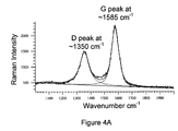
- FIG. 4A is a Raman spectrum of a layer containing carbon nanotubes in accordance with some embodiments.
- FIG. 4B is a schematic diagram of the experimental configuration for obtaining the Raman spectra in FIGS. 4A , 4 C & 4 D in accordance with some embodiments.
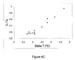
- FIG. 4C is a plot of the Raman intensity ratio I D /I G versus thermal performance for layers containing carbon nanotubes, where I D is the intensity of the D peak at ⁇ 1350 cm ⁇ 1 and is the intensity of the I G peak at ⁇ 1585 cm ⁇ 1 , in accordance with some embodiments.
- FIG. 4D shows Raman spectra of a layer containing carbon nanotubes with and without paraffin between the carbon nanotubes in accordance with some embodiments.
- FIG. 5 is a flow diagram illustrating a process for making a copper substrate with a layer containing carbon nanotubes in accordance with some embodiments.
- FIGS. 6A & 6B illustrate side and top views, respectively, of a heat spreader with a recessed cavity in accordance with some embodiments.
- FIG. 7 is a flow diagram illustrating a process for making a heat spreader with a recessed cavity in accordance with some embodiments.
- FIG. 8 illustrates a side view of an article of manufacture that includes a heat spreader with a thermal interface material in accordance with some embodiments.
- FIG. 9 is a flow diagram illustrating a process for making a heat spreader with a thermal interface material in accordance with some embodiments.
- FIG. 10 illustrates a side view of an article of manufacture that includes a heat spreader with a recessed cavity, a copper substrate, and a thermal interface material in accordance with some embodiments.
- FIG. 11 is a flow diagram illustrating a process for making an article of manufacture that includes a heat spreader with a recessed cavity, a copper substrate, and a thermal interface material in accordance with some embodiments.
- FIG. 12A is a flow diagram illustrating a process for bonding a back surface of a copper substrate to a recessed cavity in a heat spreader in accordance with some embodiments.
- FIG. 12B is a flow diagram illustrating a process for bonding a back surface of a copper substrate to a recessed cavity in a heat spreader in accordance with some embodiments.
- FIG. 13A is a flow diagram illustrating a process for placing a phase change material between carbon nanotubes in a layer containing carbon nanotubes in accordance with some embodiments.
- FIG. 13B is a flow diagram illustrating a process for placing a phase change material between carbon nanotubes in a layer containing carbon nanotubes in accordance with some embodiments.
- FIG. 14 illustrates a side view of an article of manufacture that includes a solid state-device (e.g., an integrated circuit) and a heat spreader with a thermal interface material in accordance with some embodiments.
- a solid state-device e.g., an integrated circuit
- a heat spreader with a thermal interface material in accordance with some embodiments.
- FIG. 15A is a flow diagram illustrating a process for contacting a solid state-device (e.g., an integrated circuit) with a thermal interface material in accordance with some embodiments.
- a solid state-device e.g., an integrated circuit
- FIG. 15B is a flow diagram illustrating a process for contacting an integrated circuit with a thermal interface material in accordance with some embodiments.
- FIG. 16 illustrates a side view of an article of manufacture that includes a solid state-device (e.g., an integrated circuit), a heat spreader with a recessed cavity, a copper substrate, and a thermal interface material in accordance with some embodiments.
- a solid state-device e.g., an integrated circuit
- a heat spreader with a recessed cavity e.g., a copper substrate
- a thermal interface material e.g., a thermal interface material
- FIG. 17 is a flow diagram illustrating a process for contacting a solid state-device (e.g., an integrated circuit) with a thermal interface material in accordance with some embodiments.
- a solid state-device e.g., an integrated circuit
- FIG. 18 is a flow diagram illustrating a process for removing heat from a solid state-device (e.g., an integrated circuit) in accordance with some embodiments.
- a solid state-device e.g., an integrated circuit
- FIG. 19 is a flow diagram illustrating a process for removing heat from a solid state-device (e.g., an integrated circuit) in accordance with some embodiments.
- a solid state-device e.g., an integrated circuit
- FIG. 20 is a flow diagram illustrating a process for using Raman spectroscopy to monitor thermal interface material quality in accordance with some embodiments.
- carbon nanotubes include carbon nanotubes of varying structural quality, from carbon nanotubes with few defects to carbon nanotubes with many defects (the latter of which are sometimes referred to in the art as “carbon nanofibers”). Thus, as used herein, “carbon nanotubes” include “carbon nanofibers.”
- first, second, etc. may be used herein to describe various elements, these elements should not be limited by these terms. These terms are only used to distinguish one element from another. For example, a first layer could be termed a second layer, and, similarly, a second layer could be termed a first layer, without departing from the scope of the present invention.
- relative terms such as “lower” or “bottom” and “upper” or “top,” may be used herein to describe one element's relationship to another element as illustrated in the figures. It will be understood that relative terms are intended to encompass different orientations of the device in addition to the orientation depicted in the figures. For example, if the device in one of the figures is turned over, elements described as being on the “lower” side of other elements would then be oriented on “upper” sides of the other elements. The exemplary term “lower”, can therefore, encompasses both an orientation of “lower” and “upper,” depending of the particular orientation of the figure.
- Embodiments of the invention are described herein with reference to cross-section illustrations that are schematic illustrations of idealized embodiments (and intermediate structures) of the invention. As such, variations from the shapes of the illustrations as a result, for example, of manufacturing techniques and/or tolerances, are to be expected. Thus, embodiments of the invention should not be construed as limited to the particular shapes of regions illustrated herein but are to include deviations in shapes that result, for example, from manufacturing. Thus, the regions illustrated in the figures are schematic in nature and their shapes are not intended to illustrate the actual shape of a region of a device and are not intended to limit the scope of the invention.
- FIG. 1 is a schematic cross section of an article of manufacture 100 in accordance with some embodiments.
- the article of manufacture 100 comprises a copper substrate 102 with a surface 114 .
- the copper substrate may be pure copper (e.g., electrical copper with at least 99.99% purity) or a copper alloy.
- the copper substrate 102 contains less than 40 parts per million (ppm) oxygen.
- the copper substrate 102 contains 10 ppm oxygen or less.
- the copper substrate is oxygen-free copper (OFC).
- FIG. 2 is a schematic drawing of a copper substrate 202 that is configured to fit in a recessed cavity 204 in a heat spreader 206 in accordance with some embodiments.
- the copper substrate 102 (e.g., 202 ) has a shape that is configured to fit in a recessed cavity 204 in a heat spreader 206 .
- the copper substrate has a cross-sectional area 208 and thickness 210 that substantially correspond to the cross-sectional area 212 and depth 214 of the recessed cavity 204 , respectively.
- the copper substrate cross-sectional area 208 and thickness 210 may be slightly smaller than the cross-sectional area 212 and depth 214 of the recessed cavity 204 , respectively, to allow for bonding material(s) that attach the substrate to the recessed cavity in the heat spreader.
- Typical areas 208 range from 49 mm 2 (e.g., 7 mm ⁇ 7 mm) to 2500 mm 2 (e.g., 50 mm ⁇ 50 mm).
- Typical thicknesses 210 range from 0.1 mm to 2.0 mm, with 0.5 mm to 1.0 mm being preferred.
- the heat spreader 206 is made of copper, a copper alloy, nickel-plated copper, or another high thermal conductivity substrate with a melting point above 900° C. (e.g., CuW, SiC, AlN, or graphite). In some embodiments, the heat spreader 206 does not have a rim 220 .
- the copper substrate 102 (e.g., 202 ) has a cross-sectional area 208 that substantially corresponds to the cross-sectional area of an integrated circuit or other solid-state device.
- the area of thermal interface material formed on the copper substrate can be tailored to the corresponding area of an integrated circuit or other solid-state device that will contact the thermal interface material.
- the article of manufacture 100 includes a first adhesion layer 104 that contacts the surface 114 of the copper substrate 102 .
- the first adhesion layer helps keep subsequent layers firmly attached to the copper substrate.
- the first adhesion layer 104 has a thickness between 200 and 5000 ⁇ and comprises Ti, TiN, Cr, or Ta. In some embodiments, the first adhesion layer 104 has a thickness between 200 and 500 ⁇ and comprises Ti.
- the article of manufacture 100 includes a diffusion barrier layer 106 on top of the first adhesion layer 104 .
- the diffusion barrier layer minimizes diffusion of a catalyst 110 into the copper substrate during subsequent high-temperature processing (e.g., during nanotube growth).
- the diffusion barrier layer 106 has a thickness between 100 and 400 ⁇ and comprises TiN, SiO 2 , Al 2 O 3 , or TaN. In some embodiments, the diffusion barrier layer 106 has a thickness between 100 and 400 ⁇ and comprises TiN.
- the article of manufacture 100 includes a second adhesion layer 108 between the diffusion barrier layer 106 and the catalyst 110 .
- the second adhesion layer promotes adhesion of the catalyst 110 during subsequent high-temperature processing (e.g., during nanotube growth), when thermal stresses create nucleation sites in the catalyst 110 .
- the second adhesion layer 108 has a thickness between 25 and 400 ⁇ and comprises Ti, SiO 2 , TiN, Al 2 O 3 , or Mo. In some embodiments, the second adhesion layer 108 has a thickness between 25 and 200 ⁇ and comprises Ti.
- the article of manufacture 100 includes a catalyst 110 on top of the copper substrate surface 114 .
- the catalyst catalyzes growth of the carbon nanotubes.
- the catalyst is deposited as a layer.
- the catalyst layer may subsequently form catalyst particles that act as carbon nanotube nucleation sites during the process used to form carbon nanotubes.
- the as-deposited catalyst 110 has a thickness between 30 and 1000 ⁇ and comprises Ni, Fe, or Co.
- the as-deposited catalyst 110 has a thickness between 200 and 400 ⁇ and comprises Ni.
- the article of manufacture 100 also includes a layer 112 containing carbon nanotubes 116 that contacts the catalyst 110 .
- the carbon nanotubes 116 are oriented substantially perpendicular to the surface 114 of the copper substrate. This orientation minimizes the thermal resistance of the layer 112 and of thermal interface materials that include the layer 112 .
- the carbon nanotubes 116 comprise multiwalled carbon nanotubes.
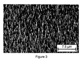
- FIG. 3 is a scanning electron microscope image of a layer containing carbon nanotubes in accordance with some embodiments.
- the carbon nanotubes 116 have an average diameter between 60 nm and 200 nm. In some embodiments, the carbon nanotubes have an average diameter between 100 nm and 150 nm. In some embodiments, the carbon nanotubes 116 have an average length between 5 and 50 ⁇ m. In some embodiments, the carbon nanotubes have an average length between 25 and 45 ⁇ m. In some embodiments, the carbon nanotubes 116 have a tip density between 10 and 40 nanotubes per ⁇ m 2 . In some embodiments, the carbon nanotubes 116 have a surface area coverage density between 15 and 40 percent.
- substantially all (e.g., >85%) of the carbon nanotubes 116 are individually separated from each other.
- axial thermal conduction of carbon nanotubes is very high, lateral thermal conduction (in the non-axial direction from nanotube to nanotube) is not as good.
- lateral contact between axially aligned nanotubes can reduce their effective axial thermal conductivity. If the number of carbon nanotubes attached to substrate is too high (for example, >40% carbon nanotube density) Van der Waals forces will create a bundle or mat situation resulting in poor thermal conduction. If, on the other hand the coverage density is too low (for example, ⁇ 15%), thermal conduction will also be lower due to the reduced number of conducting nanotubes.
- a preferred range a coverage density is between about 15 and 40%, with 25% to 40% being most preferred.
- vertically aligned, individually separated, parallel carbon nanotubes with coverage between about 15 and 40% may provide better overall thermal conduction than a bundle or mat of carbon nanotubes.
- FIG. 4A is a Raman spectrum of a layer containing carbon nanotubes in accordance with some embodiments.
- the Raman spectrum of the layer 112 containing carbon nanotubes 116 has a D peak at ⁇ 1350 cm ⁇ 1 with an intensity I D and a G peak at ⁇ 1585 cm ⁇ 1 with an intensity I G .
- FIG. 4B is a schematic diagram of the experimental configuration for obtaining the Raman spectra in FIGS. 4A , 4 C & 4 D in accordance with some embodiments.
- a ⁇ 10 mW, ⁇ 10 ⁇ m 2 laser spot was directed onto the sample with a 50 ⁇ objective lens.
- the laser spot was configured to hit the carbon nanotubes in a direction that was parallel to the axes of the carbon nanotubes.
- the Raman spectra were analyzed using Renishaw WiRE 2.0 software.
- FIG. 4C is a plot of the Raman intensity ratio I D /I G versus thermal performance for layers containing carbon nanotubes, in accordance with some embodiments.
- the thermal performance of the layer containing carbon nanotubes depends strongly on the quality of the nanotubes grown, which, in turn, depends on the materials, layers, and growth conditions used.
- Raman spectra from the layer of carbon nanotubes can be used to monitor the quality of the nanotubes.
- layers 112 with an intensity ratio I D /I G of less than 0.7 at a laser excitation wavelength of 514 nm provide good thermal performance (e.g., 0.08 cm 2 K/W or less for a 0.8 mm thick Cu substrate with layer 112 , as described below), with an intensity ratio I D /I G of less than 0.6 at a laser excitation wavelength of 514 nm being preferred.
- the intensity ratio I D /I G is plotted versus the temperature drop (Delta T, ° C.) across an ASTM 5470 thermal interface material tester containing identical copper substrates with different layers of carbon nanotubes. As shown in FIG. 4C , the temperature drop decreases (which corresponds to lower thermal resistance) as the I D /I G intensity ratio decreases.
- the Raman measurements may be taken with no interstitial material between the nanotubes (e.g., before a phase change material is placed between the carbon nanotubes or after such a phase change material is removed from between the carbon nanotubes).
- the Raman measurements may also be taken with an interstitial material between the nanotubes if the interstitial material does not interfere with the D peak at ⁇ 1350 cm ⁇ 1 and the G peak at ⁇ 1585 cm ⁇ 1 .
- FIG. 4D shows Raman spectra of a layer containing carbon nanotubes with and without paraffin between the carbon nanotubes in accordance with some embodiments. The D and G peaks in the two spectra and the corresponding I D /I G intensity ratios are essentially the same.
- a 0.8 mm thick copper substrate with a thermal interface material comprising: (a) the layer 112 containing carbon nanotubes 116 (with an average length of 25-45 ⁇ m) and (b) paraffin wax has a thermal resistance of 0.08 cm 2 K/W or less.
- This thermal resistance is a summation of: (1) the bulk thermal resistance of the copper substrate (0.02 cm 2 K/W for a 0.8 mm thick copper substrate), (2) the contact resistance at the interface between the thermal interface material and the copper substrate, (3) the bulk thermal resistance of the thermal interface material, and (4) the contact resistance at the interface between the thermal interface material and an integrated circuit or other solid-state device.
- the summation of (2)-(4) i.e., the bulk thermal resistance of the thermal interface material and the two contact resistances associated with the thermal interface material
- the summation of (2)-(4) is 0.06 cm 2 K/W or less.
- the sum of the bulk thermal resistance of the thermal interface material and the two contact resistances associated with the thermal interface material is 0.03 cm 2 K/W or less.
- the sum of the bulk thermal resistance of the thermal interface material and the two contact resistances associated with the thermal interface material is 0.02 cm 2 K/W or less.
- the sum of the bulk thermal resistance of the thermal interface material and the two contact resistances associated with the thermal interface material is between 0.02-0.06 cm 2 K/W. These values are better than what is achieved with conventional thermal interface materials and with prior thermal interface materials that include a layer of carbon nanotubes on a single surface of a copper substrate.
- the “solid-state device” referred to in the phrase “contact resistance between the thermal interface material and a/the solid-state device” may be a thermal test vehicle (TTV, e.g., a non-functional IC package that uses one or more heater resistors to simulate the power dissipation of a live IC), a heated copper block (e.g., in an ASTM D 5470 thermal interface material tester), or other equivalent to a solid-state device for testing purposes.
- TTV thermal test vehicle
- a heated copper block e.g., in an ASTM D 5470 thermal interface material tester
- the “contact resistance between the thermal interface material and a/the solid-state device” includes the contact resistance between the thermal interface material and a solid-state device (e.g., an IC, light emitting diode, laser, power transistor, RF device, or solar cell), a TTV, a copper block in a thermal interface material tester, or other equivalents to a solid-state device for testing purposes.
- a solid-state device e.g., an IC, light emitting diode, laser, power transistor, RF device, or solar cell
- TTV a copper block in a thermal interface material tester
- FIG. 5 is a flow diagram illustrating a process for making a copper substrate with a layer containing carbon nanotubes in accordance with some embodiments.
- An oxygen-free copper substrate 102 is cleaned ( 502 ).
- cleaning the oxygen-free copper substrate 102 comprises exposing the substrate 102 to a wet chemical bath.
- the wet chemical bath comprises citric acid.
- the wet chemical bath is a 100:1 mixture of 5% citric acid and hydrogen peroxide.
- cleaning the oxygen-free copper substrate 102 comprises sputter cleaning the copper substrate.
- a plasma etch step is used to remove contaminants from the oxygen-free copper substrate 102 .
- the copper substrate has a shape that is configured to fit in a recessed cavity in a heat spreader (e.g., 202 in FIG. 2 ).
- a heat spreader e.g., 202 in FIG. 2
- Using a copper substrate with this shape enables a layer of carbon nanotubes to be grown on the copper substrate in an optimum manner, without concern for how the nanotube growth conditions may alter the dimensions, surfaces, and/or mechanical properties of the heat spreader.
- a first adhesion layer 104 is formed ( 504 ) on top of the copper substrate 102 .
- a diffusion barrier layer 106 is formed ( 506 ) on top of the first adhesion layer 104 .
- a second adhesion layer 108 is formed ( 508 ) between the diffusion barrier layer 106 and the catalyst 110 .
- the second adhesion layer 108 is formed by sputtering.
- a catalyst 110 is formed ( 510 ) on top of the copper substrate 102 .
- the first adhesion layer 104 , the diffusion barrier layer 106 , the second adhesion layer 108 , and the catalyst 110 are formed by sputtering. In some embodiments, the first adhesion layer 104 , the diffusion barrier layer 106 , the second adhesion layer 108 , and the catalyst 110 are formed by sequentially sputtering each respective layer.
- the first adhesion layer 104 , the diffusion barrier layer 106 , and the catalyst 110 are formed by sputtering. If there is no second adhesion layer, in some embodiments, the first adhesion layer 104 , the diffusion barrier layer 106 , and the catalyst 110 are formed by sequentially sputtering each respective layer.
- first adhesion layer 104 may be formed using deposition methods, such as electron beam evaporation, to form the first adhesion layer 104 , the diffusion barrier layer 106 , the second adhesion layer 108 , and/or the catalyst 110 .
- the uniformity and thickness of each of these layers, especially the catalyst 110 is preferably kept within 10% total variation to promote a uniform catalyst nucleation process, which promotes individual separation of carbon nanotubes in the layer 112 containing carbon nanotubes. In some embodiments, the uniformity and thickness of the catalyst 110 is kept within 5% total variation.
- a layer 112 containing carbon nanotubes is grown ( 512 ) on the catalyst 110 .
- carbon nanotubes may form via either tip growth or base growth on the catalyst.
- growing carbon nanotubes “on the catalyst” includes tip growth, base growth, or mixtures thereof.
- growing the layer containing carbon nanotubes comprises a temperature ramp in an inert atmosphere followed by nanotube growth in a carbon-containing atmosphere.
- the temperature ramp includes ramping the temperature between 600 and 800° C. in 5 minutes or less. In some embodiments, the temperature ramp includes ramping the temperature between 600 and 800° C. in 2 minutes or less. We have found that a fast temperature ramp between 600 and 800° C. promotes a uniform catalyst nucleation process, which promotes individual separation of carbon nanotubes in the layer 112 containing carbon nanotubes.
- the inert atmosphere comprises argon or nitrogen.
- nanotube growth in the carbon-containing atmosphere comprises plasma-enhanced chemical vapor deposition (PECVD) of carbon nanotubes.
- PECVD plasma-enhanced chemical vapor deposition
- the PECVD comprises flowing NH 3 and C 2 H 2 gases over the catalyst at a temperature between 700 and 900° C. in a total pressure between 1 and 10 torr.
- An electric field created by a DC plasma may be used to align the carbon nanotubes during the PECVD growth process.
- nanotube growth in the carbon-containing atmosphere comprises thermal chemical vapor deposition (CVD) of carbon nanotubes.
- the carbon nanotubes are annealed after the growth process to release thermal stresses and to remove defects in the nanotube layer (e.g., at temperatures ranging from 700° C. to 1000° C.).
- a Raman spectrum of the layer containing carbon nanotubes has a D peak at ⁇ 1350 cm ⁇ 1 with an intensity I D , a G peak at ⁇ 1585 cm ⁇ 1 with an intensity I G , and an intensity ratio I D /I G of less than 0.7 at a laser excitation wavelength of 514 nm. In some embodiments, the intensity ratio I D /I G is less than 0.6.
- FIGS. 6A & 6B illustrate side and top views, respectively, of a heat spreader 600 with a recessed cavity 602 in accordance with some embodiments.
- the recessed cavity 602 is configured to incorporate a substrate with a thermal interface material (e.g., 102 and/or 202 ).
- the heat spreader 600 , 206 does not have a rim 620 .
- the heat spreader 600 comprises copper, the substrate (e.g., 102 and/or 202 ) comprises copper, and the thermal interface material comprises carbon nanotubes (e.g., 116 ).
- the copper may be pure copper or a copper alloy.
- the cavity 602 , 204 has a cross-sectional area (e.g., 212 ) that substantially corresponds to the cross-sectional area of an integrated circuit or other solid-state device. In some embodiments, the cavity 602 , 204 has a depth (e.g., 214 ) that substantially corresponds to the thickness of the substrate (e.g., 210 ). In some embodiments, the cavity 602 , 204 has a depth that substantially corresponds to a combined thickness of a bonding layer and the substrate. In some embodiments, the cavity 602 , 204 has a depth of 1 mm or less.
- the cavity includes one or more grooves 604 configured to contain excess material for bonding the substrate (e.g., 102 or 202 ) in the cavity.
- the substrate 202 has a cross-sectional area 208 and thickness 210 that substantially correspond to the cross-sectional area 204 and depth 214 of the recessed cavity 602 , 204 .
- FIG. 7 is a flow diagram illustrating a process for making a heat spreader with a recessed cavity in accordance with some embodiments.
- a recessed cavity is formed ( 702 ) in a heat spreader.
- the recessed cavity is configured to incorporate a substrate with an attached thermal interface material.
- the cavity is formed by machining the heat spreader.
- the cavity is formed by coining, stamping or injection molding.
- one or more grooves are formed ( 704 ) in the cavity.
- the grooves are configured to contain excess material (e.g., indium or an indium alloy) for bonding the substrate in the cavity.
- FIG. 8 illustrates a side view of an article of manufacture 800 that includes a heat spreader 802 with a thermal interface material 804 in accordance with some embodiments.
- the heat spreader 802 does not have a rim 820 .
- the heat spreader 800 comprises copper or other high-thermal conductivity metal.
- the copper may comprise pure copper, an alloy containing copper, a mixture containing copper (e.g., Cu—W), and/or a composite containing copper (e.g., Cu—Mo laminate) whose shape and mechanical properties remain substantially the same before and after carbon nanotube formation at elevated temperatures.
- the heat spreader 802 has a surface 806 that is configured to face an integrated circuit or other solid-state device.
- the thermal interface material 804 which is attached to the heat spreader 802 , comprises a layer of carbon nanotubes 808 .
- the carbon nanotubes 808 are oriented substantially perpendicular to the surface 806 of the heat spreader that is configured to face an integrated circuit or other solid-state-device.
- a Raman spectrum of the layer of carbon nanotubes has a D peak at ⁇ 1350 cm ⁇ 1 with an intensity I D , a G peak at ⁇ 1585 cm ⁇ 1 with an intensity I G , and an intensity ratio I D /I G of less than 0.7 at a laser excitation wavelength of 514 nm. In some embodiments, the intensity ratio I D /I G is less than 0.6.
- the thermal interfaced material 804 is attached to the heat spreader 802 by growing the layer of carbon nanotubes 808 on the heat spreader 802 ( FIG. 9 ).
- a field mask may be used to restrict carbon nanotube growth to a particular area on the heat spreader.
- the thermal interface material is attached to the heat spreader by growing the layer of carbon nanotubes on a copper substrate and attaching the copper substrate to the heat spreader (e.g., FIGS. 10 & 11 ).
- the copper substrate is attached to the heat spreader by bonding the substrate to a recessed cavity in the heat spreader.
- the thermal interface material 804 comprises a phase change material located between the carbon nanotubes 808 .
- the phase change material comprises a wax.
- the phase change material comprises paraffin. We believe that phase change materials like paraffin improve the thermal performance of the thermal interface material 804 by filling the air gap between carbon nanotubes with lengths that do not make thermal contact with an opposing IC or other solid-state device surface and by wetting and separating the carbon nanotubes when pressed to conform with asperities on the opposing surface.
- the article of manufacture 800 may be reworkable, which increases yields and reduces manufacturing costs.
- an integrated circuit or other solid-state device may be removably connected to the thermal interface material 804 .
- the thermal interface material 804 is configured to enable an integrated circuit or other solid-state device to be connected to the thermal interface material, disconnected from the thermal interface material, and then reconnected to the thermal interface material.
- the article of manufacture 800 is configured to be reused to cool a succession of integrated circuits or other solid-state devices.
- the summation of the bulk thermal resistance of the thermal interface material 804 and the two contact resistances associated with the thermal interface material is 0.06 cm 2 K/W or less. In some embodiments, the summation of the bulk thermal resistance of the thermal interface material 804 and the two contact resistances associated with the thermal interface material is 0.03 cm 2 K/W or less. In some embodiments, the summation of the bulk thermal resistance of the thermal interface material and the two contact resistances associated with the thermal interface material is 0.02 cm 2 K/W or less. In some embodiments, the summation has a value between 0.02-0.06 cm 2 K/W. These values are better than what is achieved with conventional thermal interface materials and with prior thermal interface materials that include a layer of carbon nanotubes on a single surface of a copper substrate.
- FIG. 9 is a flow diagram illustrating a process for making a heat spreader 802 with a thermal interface material 804 in accordance with some embodiments.
- the process described here is analogous to that described in FIG. 5 , except a field mask may be used to restrict carbon nanotube growth to a particular area on the heat spreader.
- the surface 806 of a heat spreader 802 is cleaned ( 902 ).
- the heat spreader 802 comprises copper with less than 40 ppm oxygen. In some embodiments, the heat spreader 802 comprises copper with 10 ppm oxygen or less.
- cleaning the surface of the heat spreader comprises exposing the surface of the heat spreader to a wet chemical bath.
- the wet chemical bath comprises citric acid.
- the wet chemical bath is a 100:1 mixture of 5% citric acid and hydrogen peroxide.
- cleaning the surface of the heat spreader comprises sputter cleaning the surface of the heat spreader.
- a plasma etch step is used to remove contaminants from the surface of the heat spreader.
- a first adhesion layer is formed ( 904 ) on top of the surface of the heat spreader.
- a diffusion barrier layer is formed ( 906 ) on top of the first adhesion layer.
- a second adhesion layer is formed ( 908 ) between the diffusion barrier layer and a catalyst.
- the second adhesion layer is formed by sputtering.
- a catalyst is formed ( 910 ) on top of the surface 806 of the heat spreader.
- the first adhesion layer, the diffusion barrier layer, the second adhesion layer, and the catalyst are formed by sputtering. In some embodiments, the first adhesion layer, the diffusion barrier layer, the second adhesion layer, and the catalyst are formed by sequentially sputtering each respective layer.
- the first adhesion layer, the diffusion barrier layer, and the catalyst are formed by sputtering. If there is no second adhesion layer, in some embodiments, the first adhesion layer, the diffusion barrier layer, and the catalyst are formed by sequentially sputtering each respective layer.
- first adhesion layer may be formed using deposition methods, such as electron beam evaporation, to form the first adhesion layer, the diffusion barrier layer, the second adhesion layer, and/or the catalyst.
- the uniformity and thickness of each of these layers, especially the catalyst is preferably kept within 10% total variation to promote a uniform catalyst nucleation process, which promotes individual separation of carbon nanotubes in the layer containing carbon nanotubes. In some embodiments, the uniformity and thickness of the catalyst is kept within 5% total variation.
- a layer containing carbon nanotubes is grown ( 912 ) on the catalyst.
- carbon nanotubes may form via either tip growth or base growth on the catalyst.
- growing carbon nanotubes “on the catalyst” includes tip growth, base growth, or mixtures thereof.
- a Raman spectrum of the layer containing carbon nanotubes has a D peak at ⁇ 1350 cm ⁇ 1 with an intensity I D , a G peak at ⁇ 1585 cm ⁇ 1 with an intensity I G , and an intensity ratio I D /I G of less than 0.7 at a laser excitation wavelength of 514 nm. In some embodiments, the intensity ratio I D /I G is less than 0.6.
- growing the layer containing carbon nanotubes comprises a temperature ramp in an inert atmosphere followed by nanotube growth in a carbon-containing atmosphere.
- the temperature ramp includes ramping the temperature between 600 and 800° C. in 5 minutes or less. In some embodiments, the temperature ramp includes ramping the temperature between 600 and 800° C. in 2 minutes or less. We have found that a fast temperature ramp between 600 and 800° C. promotes a uniform catalyst nucleation process, which promotes individual separation of carbon nanotubes in the layer 112 containing carbon nanotubes.
- the inert atmosphere comprises argon or nitrogen.
- nanotube growth in the carbon-containing atmosphere comprises plasma-enhanced chemical vapor deposition (PECVD) of carbon nanotubes.
- PECVD plasma-enhanced chemical vapor deposition
- the PECVD comprises flowing NH 3 and C 2 H 2 gases over the catalyst at a temperature between 700 and 900° C. in a total pressure between 1 and 10 torr.
- An electric field created by a DC plasma may be used to align the carbon nanotubes during the PECVD growth process.
- nanotube growth in the carbon-containing atmosphere comprises thermal chemical vapor deposition (CVD) of carbon nanotubes.
- the carbon nanotubes are annealed after the growth process to release thermal stresses and to remove defects in the nanotube layer (e.g., at temperatures ranging from 700° C. to 1000° C.).
- a phase change material is placed ( 914 ) between carbon nanotubes in the layer containing carbon nanotubes.
- the phase change material comprises a wax.
- the phase change material comprises paraffin.
- adsorption via capillary forces is used to place the phase change material in the space between the carbon nanotubes.
- FIG. 10 illustrates a side view of an article of manufacture 1000 that includes a heat spreader 1002 with a recessed cavity 1014 , a copper substrate 1004 , and a thermal interface material 1006 in accordance with some embodiments.
- the heat spreader 1002 does not have a rim 1020 .
- the copper substrate 1004 has a front surface 1008 and a back surface 1010 .
- the back surface 1010 is bonded to the recessed cavity 1014 .
- the thermal interface material 1006 which is attached to the front surface 1008 of the copper substrate, comprises a layer of carbon nanotubes 1012 .
- the carbon nanotubes are oriented substantially perpendicular to the front surface of the copper substrate.
- the copper substrate 1004 substantially fills the recessed cavity 1014 .
- the thermal interface material 1006 further comprises a phase change material located between the carbon nanotubes 1012 .
- the phase change material comprises a wax.
- the phase change material comprises paraffin. We believe that phase change materials like paraffin improve the thermal performance of the thermal interface material 1006 by filling the air gap between carbon nanotubes with lengths that do not make thermal contact with an opposing IC or other solid-state device surface and by wetting and separating the carbon nanotubes when pressed to conform with asperities on the opposing surface.
- the layer of carbon nanotubes 1012 are attached to the front surface 1008 of the copper substrate by growing the nanotubes on the front surface of the copper substrate (e.g., as described with respect to FIG. 5 ).
- substantially all of the carbon nanotubes 1012 are individually separated from each other, as described above.
- a Raman spectrum of the layer of carbon nanotubes has a D peak at ⁇ 1350 cm ⁇ 1 with an intensity I D , a G peak at ⁇ 1585 cm ⁇ 1 with an intensity I G , and an intensity ratio I D /I G of less than 0.7 at a laser excitation wavelength of 514 nm. In some embodiments, the intensity ratio I D /I G is less than 0.6.
- the summation of the bulk thermal resistance of the thermal interface material 1006 and the two contact resistances associated with the thermal interface material is 0.06 cm 2 K/W or less. In some embodiments, the summation of the bulk thermal resistance of the thermal interface material 804 and the two contact resistances associated with the thermal interface material is 0.03 cm 2 K/W or less. In some embodiments, the summation of the bulk thermal resistance of the thermal interface material and the two contact resistances associated with the thermal interface material is 0.02 cm 2 K/W or less. In some embodiments, the summation has a value between 0.02-0.06 cm 2 K/W. These values are better than what is achieved with conventional thermal interface materials and with prior thermal interface materials that include a layer of carbon nanotubes on a single surface of a copper substrate.
- FIG. 11 is a flow diagram illustrating a process for making an article of manufacture 1000 that includes a heat spreader 1002 with a recessed cavity 1014 , a copper substrate 1004 , and a thermal interface material 1006 in accordance with some embodiments.
- a layer containing carbon nanotubes 1012 is grown ( 1102 ) on top of a front surface 1008 of a copper substrate 1004 (e.g., as described with respect to FIG. 5 ).
- the layer of carbon nanotubes 1012 are oriented substantially perpendicular to the front surface 1008 of the copper substrate 1004 .
- a Raman spectrum of the layer of carbon nanotubes 1012 has a D peak at ⁇ 1350 cm ⁇ 1 with an intensity I D , a G peak at ⁇ 1585 cm ⁇ 1 with an intensity I G , and an intensity ratio I D /I G of less than 0.7 at a laser excitation wavelength of 514 nm. In some embodiments, the intensity ratio I D /I G is less than 0.6.
- the back surface 1010 of the copper substrate 1004 is bonded ( 1104 ) to the recessed cavity 1014 in the heat spreader 1002 .
- a phase change material is placed ( 1106 ) between carbon nanotubes in the layer containing carbon nanotubes.
- the phase change material comprises paraffin.
- the carbon nanotubes are planarized (e.g., by chemical mechanical polishing, microtoming, or plasma etching).
- FIG. 12A is a flow diagram illustrating a process for bonding ( 1202 ) a back surface 1010 of a copper substrate 1004 to a recessed cavity 1014 in a heat spreader 1002 in accordance with some embodiments.
- a thermal interface material 1006 is attached to the front surface 1008 of the copper substrate 1004 .
- the thermal interface material 1006 comprises a layer of carbon nanotubes 1012 oriented substantially perpendicular to the front surface of the copper substrate.
- FIG. 12B is a flow diagram illustrating a process for bonding a back surface 1010 of a copper substrate 1004 to a recessed cavity 1014 in a heat spreader 1002 in accordance with some embodiments.
- the bonding comprises:
- the bonding comprises microwave bonding (e.g., as disclosed in U.S. Pat. Nos. 6,734,409 and 6,809,305), tin-lead solder bonding, or reactive bonding (e.g., as disclosed in U.S. Pat. No. 5,381,944).
- FIG. 13A is a flow diagram illustrating a process for placing ( 1302 ) a phase change material between carbon nanotubes in a layer containing carbon nanotubes in accordance with some embodiments.
- a Raman spectrum of the layer containing carbon nanotubes has a D peak at ⁇ 1350 cm ⁇ 1 with an intensity I D , a G peak at ⁇ 1585 cm ⁇ 1 with an intensity I G , and an intensity ratio I D /I G of less than 0.7 at a laser excitation wavelength of 514 nm.
- the intensity ratio I D /I G is less than 0.6.
- FIG. 13B is a flow diagram illustrating a process for placing a phase change material between carbon nanotubes in a layer containing carbon nanotubes in accordance with some embodiments.
- the placing comprises:
- FIG. 14 illustrates a side view of an article of manufacture 1400 that includes a solid-state device (e.g., integrated circuit 1410 ) and a heat spreader 1402 with a thermal interface material 1404 in accordance with some embodiments.
- a solid-state device e.g., integrated circuit 1410
- a heat spreader 1402 with a thermal interface material 1404 in accordance with some embodiments.
- the printed circuit board or other substrate that the integrated circuit 1410 is attached to is omitted for clarity.
- Article 1400 can further include additional components (not shown).
- the heat spreader 1402 has a surface 1406 facing the integrated circuit 1410 .
- the thermal interface material 1404 is attached to the heat spreader 1402 .
- the thermal interface material 1404 contacts the integrated circuit 1410 .
- the thermal interface material 1404 comprises a layer of carbon nanotubes 1408 .
- the carbon nanotubes are oriented substantially perpendicular to the surface 1406 of the heat spreader facing the integrated circuit.
- a field mask may be used to restrict carbon nanotube growth to a particular area on the heat spreader.
- a Raman spectrum of the layer of carbon nanotubes has a D peak at ⁇ 1350 cm ⁇ with an intensity I D , a G peak at ⁇ 1585 cm ⁇ with an intensity I G , and an intensity ratio I D /I G of less than 0.7 at a laser excitation wavelength of 514 nm. In some embodiments, the intensity ratio I D /I G is less than 0.6.
- the article of manufacture is a computer, such as a server computer, client computer, desktop computer, laptop computer, handheld computer, personal digital assistant, cell phone, gaming console, or handheld gaming device.
- FIG. 15A is a flow diagram illustrating a process for contacting ( 1502 ) a solid-state device (e.g., integrated circuit 1410 ) with a thermal interface material 1404 in accordance with some embodiments.
- the thermal interface material 1404 is attached to a surface 1406 of a heat spreader 1402 .
- the thermal interface material 1404 comprises a layer of carbon nanotubes 1408 that are oriented substantially perpendicular to the surface 1406 of the heat spreader 1402 .
- a Raman spectrum of the layer of carbon nanotubes has a D peak at ⁇ 1350 cm ⁇ 1 with an intensity I D , a G peak at ⁇ 1585 cm ⁇ 1 with an intensity I G , and an intensity ratio I D /I G of less than 0.7 at a laser excitation wavelength of 514 nm. In some embodiments, the intensity ratio I D /I G is less than 0.6.
- the heat spreader 1402 and thermal interface material 1404 may be reworkable, which increases yields and reduces manufacturing costs. In some embodiments, contact between the solid-state device and the thermal interface material 1404 is broken ( 1504 ), and then contact between the solid-state device and the thermal interface material is reestablished ( 1506 ).
- FIG. 15B is a flow diagram illustrating a process for contacting an integrated circuit with a thermal interface material in accordance with some embodiments.
- the contacting comprises:
- an adhesive to a rim (e.g., 220 , 620 , 820 , 1020 , 1420 , or 1620 ) of the heat spreader;
- the layer of carbon nanotubes in the thermal interface material is designed to have sufficient compressibility so that the nanotubes contact the entire integrated circuit surface even if there are deviations in the flatness of the integrated circuit surface.
- the layer of carbon nanotubes can be made with an average length of 30-50 ⁇ m, an average diameter of 100-150 nm, and a Young's Modulus of 30-150 GPa so that the thermal resistance is low (e.g., 0.06 cm 2 K/W or less) when a pressure of 30-50 psi is applied to the heat spreader.
- FIG. 16 illustrates a side view of an article of manufacture 1600 that includes a solid-state device (e.g., integrated circuit 1616 ), a heat spreader 1602 with a recessed cavity 1614 , a copper substrate 1604 , and a thermal interface material 1606 in accordance with some embodiments.
- a solid-state device e.g., integrated circuit 1616
- heat spreader 1602 with a recessed cavity 1614 e.g., integrated circuit 1616
- a copper substrate 1604 e.g., copper substrate 1604
- thermal interface material 1606 e.g., thermal interface material
- the copper substrate 1604 has a front surface 1608 and a back surface 1610 .
- the back surface 1610 is bonded to the recessed cavity 1614 .
- the thermal interface material 1606 is attached to the front surface 1608 of the copper substrate 1640 .
- the thermal interface material 1606 contacts the integrated circuit 1616 .
- the thermal interface material 1606 comprises a layer of carbon nanotubes 1612 .
- the carbon nanotubes are oriented substantially perpendicular to the front surface 1608 of the copper substrate 1604 .
- the article of manufacture is a computer, such as a server computer, client computer, desktop computer, laptop computer, handheld computer, personal digital assistant, cell phone, gaming console, or handheld gaming device.
- FIG. 17 is a flow diagram illustrating a process for contacting ( 1702 ) a solid-state device (e.g., integrated circuit 1616 ) with a thermal interface material 1606 in accordance with some embodiments.
- the thermal interface material 1606 is attached to a copper substrate 1604 with a front surface 1608 and a back surface 1610 .
- the thermal interface material 1606 comprises a layer of carbon nanotubes 1612 that are oriented substantially perpendicular to the front surface 1608 of the copper substrate 1604 .
- the back surface 1610 of the copper substrate 1604 is bonded to a recessed cavity 1614 in a heat spreader 1602 .
- the contacting comprises the steps described above with respect to FIG. 15B .
- FIG. 18 is a flow diagram illustrating a process for removing heat from a solid-state device (e.g. integrated circuit 1410 ) in accordance with some embodiments.
- a solid-state device e.g. integrated circuit 1410
- Heat is generated ( 1802 ) in a solid-state device (e.g., during the use of a computer containing integrated circuit 1410 ).
- At least some of the heat is conducted ( 1804 ) away from the solid-state device via a thermal interface material 1404 and a heat spreader 1402 with a surface 1406 facing the solid-state device.
- the thermal interface material 1404 comprises a layer of carbon nanotubes 1408 oriented substantially perpendicular to the surface 1406 of the heat spreader facing the solid-state device.
- a Raman spectrum of the layer of carbon nanotubes has a D peak at ⁇ 1350 cm ⁇ 1 with an intensity I D , a G peak at ⁇ 1585 cm ⁇ 1 with an intensity I G , and an intensity ratio I D /I G of less than 0.7 at a laser excitation wavelength of 514 nm. In some embodiments, the intensity ratio I D /I G is less than 0.6.
- FIG. 19 is a flow diagram illustrating a process for removing heat from a solid-state device (e.g., integrated circuit 1616 ) in accordance with some embodiments.
- a solid-state device e.g., integrated circuit 1616
- Heat is generated ( 1902 ) in a solid-state device (e.g., during the use of a computer containing integrated circuit 1616 ).
- At least some of the heat is conducted ( 1904 ) away from the solid-state device via a thermal interface material 1606 attached to a copper substrate 1604 .
- the copper substrate 1604 is bonded to a recessed cavity 1614 in a heat spreader 1602 .
- FIG. 20 is a flow diagram illustrating a process for using Raman spectroscopy to monitor thermal interface material quality in accordance with some embodiments.
- a Raman spectrum is obtained ( 2002 ) from an article of manufacture that comprises a thermal interface material with a layer of carbon nanotubes.
- the Raman spectrum of the layer of carbon nanotubes has a D peak at ⁇ 1350 cm ⁇ 1 with an intensity I D and a G peak at ⁇ 1585 cm ⁇ 1 with an intensity I G .
- the article of manufacture comprises a copper substrate (e.g., 202 ) with a shape that is configured to fit in a recessed cavity in a heat spreader.
- the article of manufacture comprises a heat spreader (e.g., 802 ).
- the article of manufacture is accepted ( 2004 ) if the Raman spectrum has an intensity ratio I D /I G less than a predetermined value.
- the predetermined value is 0.7. In some embodiments, the predetermined value is 0.6.
- the article of manufacture is rejected ( 2006 ) if the Raman spectrum has an intensity ratio I D /I G greater than the predetermined value.
- articles of manufacture with thermal interface materials based on carbon nanotubes can be easily screened with Raman spectroscopy.
Abstract
Description
-
- forming (1204) a gold or gold alloy adhesion layer in recessed cavity 1014 (e.g., by sputtering or electron evaporation);
- placing (1206) spacers (e.g., 25 μm diameter copper wire) in the recessed
cavity 1014; - placing (1208) indium or an indium alloy in the recessed cavity (e.g., a 50 μm thick indium foil for a (50−25=) 25 μm bond line thickness);
- placing (1210) the copper substrate 1004 in the recessed
cavity 1014; - melting (1212) the indium or indium alloy;
- applying (1214) pressure to the copper substrate (e.g., applying 2-5 lb. pressure); and
- solidifying (1216) the indium or indium alloy (e.g., by cooling to room temperature).
-
- dehydrating (1304) the carbon nanotubes (e.g., by placing an article with the layer containing carbon nanotubes on a heated surface at 100° C. for 5 minutes);
- contacting (1306) the carbon nanotubes with a source of phase change material (e.g., for paraffin wax, pressing a pre-waxed paper on to the tips of the carbon nanotubes with a flat surface at a temperature above the melting point of the paraffin wax);
- reflowing (1308) the phase change material;
- cooling (1310) the carbon nanotubes and phase change material (e.g., by quenching on a metal block); and
- optionally, reflowing (1312) the phase change material again and cooling (1314) the carbon nanotubes and phase change material one or more additional times.
Claims (22)
Priority Applications (1)
| Application Number | Priority Date | Filing Date | Title |
|---|---|---|---|
| US12/177,815 US8080871B2 (en) | 2003-08-25 | 2008-07-22 | Carbon nanotube-based structures and methods for removing heat from solid-state devices |
Applications Claiming Priority (5)
| Application Number | Priority Date | Filing Date | Title |
|---|---|---|---|
| US49784903P | 2003-08-25 | 2003-08-25 | |
| US10/925,824 US7109581B2 (en) | 2003-08-25 | 2004-08-24 | System and method using self-assembled nano structures in the design and fabrication of an integrated circuit micro-cooler |
| US11/498,408 US8039953B2 (en) | 2003-08-25 | 2006-08-02 | System and method using self-assembled nano structures in the design and fabrication of an integrated circuit micro-cooler |
| US74911607A | 2007-05-15 | 2007-05-15 | |
| US12/177,815 US8080871B2 (en) | 2003-08-25 | 2008-07-22 | Carbon nanotube-based structures and methods for removing heat from solid-state devices |
Related Parent Applications (1)
| Application Number | Title | Priority Date | Filing Date |
|---|---|---|---|
| US74911607A Continuation | 2003-08-25 | 2007-05-15 |
Publications (2)
| Publication Number | Publication Date |
|---|---|
| US20110103020A1 US20110103020A1 (en) | 2011-05-05 |
| US8080871B2 true US8080871B2 (en) | 2011-12-20 |
Family
ID=34221520
Family Applications (1)
| Application Number | Title | Priority Date | Filing Date |
|---|---|---|---|
| US12/177,815 Active 2026-02-08 US8080871B2 (en) | 2003-08-25 | 2008-07-22 | Carbon nanotube-based structures and methods for removing heat from solid-state devices |
Country Status (1)
| Country | Link |
|---|---|
| US (1) | US8080871B2 (en) |
Cited By (4)
| Publication number | Priority date | Publication date | Assignee | Title |
|---|---|---|---|---|
| US8952258B2 (en) | 2012-09-21 | 2015-02-10 | International Business Machines Corporation | Implementing graphene interconnect for high conductivity applications |
| US9601904B1 (en) | 2015-12-07 | 2017-03-21 | Raytheon Company | Laser diode driver with variable input voltage and variable diode string voltage |
| US10764989B1 (en) * | 2019-03-25 | 2020-09-01 | Dialog Semiconductor (Uk) Limited | Thermal enhancement of exposed die-down package |
| US11417585B2 (en) | 2016-11-30 | 2022-08-16 | Whirlpool Corporation | System for cooling components in an electronic module |
Families Citing this family (22)
| Publication number | Priority date | Publication date | Assignee | Title |
|---|---|---|---|---|
| JP4881352B2 (en) * | 2008-08-11 | 2012-02-22 | ソニー株式会社 | HEAT SPREADER, ELECTRONIC DEVICE, AND HEAT SPREADER MANUFACTURING METHOD |
| JP4623167B2 (en) * | 2008-08-26 | 2011-02-02 | トヨタ自動車株式会社 | Heat dissipation structure and vehicle inverter |
| JP2010062234A (en) * | 2008-09-02 | 2010-03-18 | Sony Corp | Heat spreader, electronic equipment and method of manufacturing heat spreader |
| JP2010171200A (en) * | 2009-01-22 | 2010-08-05 | Shinko Electric Ind Co Ltd | Heat radiator of semiconductor package |
| JP2010243036A (en) * | 2009-04-03 | 2010-10-28 | Sony Corp | Heat transport device, electronic apparatus and method of manufacturing the heat transport device |
| US8508943B2 (en) * | 2009-10-16 | 2013-08-13 | Raytheon Company | Cooling active circuits |
| EP2739929A4 (en) * | 2011-08-03 | 2015-09-02 | Anchor Science Llc | Dynamic thermal interface material |
| TW201418156A (en) * | 2012-10-26 | 2014-05-16 | Applied Materials Inc | Carbon nanotube growth on copper substrates |
| CN203243595U (en) * | 2013-03-07 | 2013-10-16 | 杭州华三通信技术有限公司 | A pcb structure |
| JP6094015B2 (en) * | 2013-04-12 | 2017-03-15 | ホシデン株式会社 | Terminal box |
| US20140326856A1 (en) * | 2013-05-06 | 2014-11-06 | Omnivision Technologies, Inc. | Integrated circuit stack with low profile contacts |
| FR3011067B1 (en) * | 2013-09-23 | 2016-06-24 | Commissariat Energie Atomique | APPARATUS COMPRISING A FUNCTIONAL COMPONENT LIKELY TO BE OVERHEAD WHEN OPERATING AND A COMPONENT COOLING SYSTEM |
| US8912637B1 (en) * | 2013-09-23 | 2014-12-16 | Texas Instruments Incorporated | Self-adhesive die |
| US20150201486A1 (en) * | 2014-01-16 | 2015-07-16 | Whelen Engineering Company, Inc. | Stacked Heatsink Assembly |
| US9613882B2 (en) * | 2014-07-28 | 2017-04-04 | Northrop Grumman Systems Corporation | Nanoparticle thermal interface agents for reducing thermal conductance resistance |
| CN106996831B (en) * | 2016-01-22 | 2020-02-07 | 清华大学 | Sensor for specific light wavelength |
| CN106996832B (en) * | 2016-01-22 | 2019-09-27 | 清华大学 | Optical wavelength detector and application method |
| US9918407B2 (en) * | 2016-08-02 | 2018-03-13 | Qualcomm Incorporated | Multi-layer heat dissipating device comprising heat storage capabilities, for an electronic device |
| US10188015B2 (en) * | 2016-09-20 | 2019-01-22 | Qualcomm Incorporated | Hybrid design of heat spreader and temperature sensor for direct handheld device skin temperature measurement |
| US10405465B2 (en) * | 2017-11-16 | 2019-09-03 | The Boeing Company | Topological insulator thermal management systems |
| US10901030B2 (en) * | 2019-02-19 | 2021-01-26 | International Business Machines Corporation | Viscoelastic pad upon integrated circuit device contact for multipass electrical characterization probe testing |
| US11495516B2 (en) * | 2020-11-20 | 2022-11-08 | Nanya Technology Corporation | Semiconductor device with thermal release layer and method for fabricating the same |
Citations (5)
| Publication number | Priority date | Publication date | Assignee | Title |
|---|---|---|---|---|
| US6110264A (en) | 1998-06-25 | 2000-08-29 | Xerox Corporation | Phase change inks and methods of forming phase change inks |
| US20030117770A1 (en) | 2001-12-20 | 2003-06-26 | Intel Corporation | Carbon nanotube thermal interface structures |
| US20050037204A1 (en) | 2003-08-13 | 2005-02-17 | Robert Osiander | Method of making carbon nanotube arrays, and thermal interfaces using same |
| WO2005041256A2 (en) | 2003-08-25 | 2005-05-06 | Nanoconduction, Inc. | An integrated circuit micro-cooler using self-assembled nano structures |
| US7168484B2 (en) * | 2003-06-30 | 2007-01-30 | Intel Corporation | Thermal interface apparatus, systems, and methods |
-
2008
- 2008-07-22 US US12/177,815 patent/US8080871B2/en active Active
Patent Citations (5)
| Publication number | Priority date | Publication date | Assignee | Title |
|---|---|---|---|---|
| US6110264A (en) | 1998-06-25 | 2000-08-29 | Xerox Corporation | Phase change inks and methods of forming phase change inks |
| US20030117770A1 (en) | 2001-12-20 | 2003-06-26 | Intel Corporation | Carbon nanotube thermal interface structures |
| US7168484B2 (en) * | 2003-06-30 | 2007-01-30 | Intel Corporation | Thermal interface apparatus, systems, and methods |
| US20050037204A1 (en) | 2003-08-13 | 2005-02-17 | Robert Osiander | Method of making carbon nanotube arrays, and thermal interfaces using same |
| WO2005041256A2 (en) | 2003-08-25 | 2005-05-06 | Nanoconduction, Inc. | An integrated circuit micro-cooler using self-assembled nano structures |
Non-Patent Citations (6)
| Title |
|---|
| Antunes et al., Carbon 44:2002-2211 (2006). |
| Gan et al., Diamond and Related Materials 9:897-900 (Apr. 2000). |
| Ngo et al., Nano Letters 4(12):2403-2407 (2004). |
| Sun, "Study of Interactions at the Atomic Scale," PhD Thesis, McGill University, Montréal, Québec, Canada, pp. 1-117 (2004). |
| Teo et al., Applied Physics Letters 80(11):2011-2013 (Mar. 18, 2002). |
| Xu et al., International Journal of Heat and Mass Transfer, pp. 1658-1666 (2006). |
Cited By (5)
| Publication number | Priority date | Publication date | Assignee | Title |
|---|---|---|---|---|
| US8952258B2 (en) | 2012-09-21 | 2015-02-10 | International Business Machines Corporation | Implementing graphene interconnect for high conductivity applications |
| US9601904B1 (en) | 2015-12-07 | 2017-03-21 | Raytheon Company | Laser diode driver with variable input voltage and variable diode string voltage |
| US9923334B2 (en) | 2015-12-07 | 2018-03-20 | Raytheon Company | Laser diode driver with variable input voltage and variable diode string voltage |
| US11417585B2 (en) | 2016-11-30 | 2022-08-16 | Whirlpool Corporation | System for cooling components in an electronic module |
| US10764989B1 (en) * | 2019-03-25 | 2020-09-01 | Dialog Semiconductor (Uk) Limited | Thermal enhancement of exposed die-down package |
Also Published As
| Publication number | Publication date |
|---|---|
| US20110103020A1 (en) | 2011-05-05 |
Similar Documents
| Publication | Publication Date | Title |
|---|---|---|
| US8080871B2 (en) | Carbon nanotube-based structures and methods for removing heat from solid-state devices | |
| US8039961B2 (en) | Composite carbon nanotube-based structures and methods for removing heat from solid-state devices | |
| US20080131722A1 (en) | Single Layer Carbon Nanotube-Based Structures and Methods for Removing Heat from Solid-State Devices | |
| US20080131655A1 (en) | Double Layer Carbon Nanotube-Based Structures and Methods for Removing Heat from Solid-State Devices | |
| US7569425B2 (en) | Method for manufacturing thermal interface material with carbon nanotubes | |
| US7538422B2 (en) | Integrated circuit micro-cooler having multi-layers of tubes of a CNT array | |
| US7109581B2 (en) | System and method using self-assembled nano structures in the design and fabrication of an integrated circuit micro-cooler | |
| JP5628312B2 (en) | Nanotube thermal interface structure | |
| US20090246507A1 (en) | Systems and methods for fabrication and transfer of carbon nanotubes | |
| EP2546871B1 (en) | Method for producing a heat dissipating structure | |
| US20070126116A1 (en) | Integrated Circuit Micro-Cooler Having Tubes of a CNT Array in Essentially the Same Height over a Surface | |
| CA2690795C (en) | Metal bonded nanotube array | |
| US20110007477A1 (en) | Enhancement of thermal interface conductivities with carbon nanotube arrays | |
| TW200951210A (en) | Sheet structure and method of manufacturing sheet structure | |
| US10177082B2 (en) | Method for forming semiconductor package using carbon nano material in molding compound | |
| US20070114658A1 (en) | Integrated Circuit Micro-Cooler with Double-Sided Tubes of a CNT Array | |
| JP7172319B2 (en) | Heat dissipation structure, electronic device, and method for manufacturing heat dissipation structure | |
| WO2007137095A2 (en) | Carbon nanotube-based structures and methods for removing heat from solid-state devices | |
| JP2006245235A (en) | Structure and semiconductor element heat dissipation member using same, and semiconductor device | |
| JP2009253123A (en) | Heat dissipation structure manufacturing method | |
| JP4919357B2 (en) | Manufacturing method of electronic device | |
| TWM407489U (en) | IC carrier board with high thermal conductivity, packaging IC carrier board, and electronic devices | |
| JP5010640B2 (en) | Laminated structure using metal matrix composite | |
| Hansson | Exploration of Metal Composites and Carbon Nanotubes for Thermal Interfaces | |
| JP5287237B2 (en) | Device structure of carbon fiber and manufacturing method thereof |
Legal Events
| Date | Code | Title | Description |
|---|---|---|---|
| AS | Assignment |
Owner name: NANOCONDUCTION, INC., CALIFORNIA Free format text: ASSIGNMENT OF ASSIGNORS INTEREST;ASSIGNORS:DANGELO, CARLOS;SUHIR, EPHRAIM;WACKER, BARBARA;AND OTHERS;SIGNING DATES FROM 20070516 TO 20070801;REEL/FRAME:021739/0394 |
|
| AS | Assignment |
Owner name: UNIDYM, INC., CALIFORNIA Free format text: ASSIGNMENT OF ASSIGNORS INTEREST;ASSIGNOR:NANOCONDUCTION, INC.;REEL/FRAME:025390/0874 Effective date: 20101118 |
|
| AS | Assignment |
Owner name: SAMSUNG ELECTRONICS CO., LTD., KOREA, REPUBLIC OF Free format text: ASSIGNMENT OF ASSIGNORS INTEREST;ASSIGNOR:UNIDYM, INC.;REEL/FRAME:025875/0331 Effective date: 20110227 |
|
| STCF | Information on status: patent grant |
Free format text: PATENTED CASE |
|
| FEPP | Fee payment procedure |
Free format text: PAYOR NUMBER ASSIGNED (ORIGINAL EVENT CODE: ASPN); ENTITY STATUS OF PATENT OWNER: LARGE ENTITY |
|
| FPAY | Fee payment |
Year of fee payment: 4 |
|
| MAFP | Maintenance fee payment |
Free format text: PAYMENT OF MAINTENANCE FEE, 8TH YEAR, LARGE ENTITY (ORIGINAL EVENT CODE: M1552); ENTITY STATUS OF PATENT OWNER: LARGE ENTITY Year of fee payment: 8 |
|
| MAFP | Maintenance fee payment |
Free format text: PAYMENT OF MAINTENANCE FEE, 12TH YEAR, LARGE ENTITY (ORIGINAL EVENT CODE: M1553); ENTITY STATUS OF PATENT OWNER: LARGE ENTITY Year of fee payment: 12 |