EP1329949A2 - Semiconductor device and method of manufacturing semiconductor device - Google Patents
Semiconductor device and method of manufacturing semiconductor device Download PDFInfo
- Publication number
- EP1329949A2 EP1329949A2 EP03001196A EP03001196A EP1329949A2 EP 1329949 A2 EP1329949 A2 EP 1329949A2 EP 03001196 A EP03001196 A EP 03001196A EP 03001196 A EP03001196 A EP 03001196A EP 1329949 A2 EP1329949 A2 EP 1329949A2
- Authority
- EP
- European Patent Office
- Prior art keywords
- bonding
- substrate
- resin
- hole
- semiconductor device
- Prior art date
- Legal status (The legal status is an assumption and is not a legal conclusion. Google has not performed a legal analysis and makes no representation as to the accuracy of the status listed.)
- Withdrawn
Links
Images




Classifications
-
- H—ELECTRICITY
- H10—SEMICONDUCTOR DEVICES; ELECTRIC SOLID-STATE DEVICES NOT OTHERWISE PROVIDED FOR
- H10W—GENERIC PACKAGES, INTERCONNECTIONS, CONNECTORS OR OTHER CONSTRUCTIONAL DETAILS OF DEVICES COVERED BY CLASS H10
- H10W72/00—Interconnections or connectors in packages
- H10W72/071—Connecting or disconnecting
-
- H—ELECTRICITY
- H10—SEMICONDUCTOR DEVICES; ELECTRIC SOLID-STATE DEVICES NOT OTHERWISE PROVIDED FOR
- H10W—GENERIC PACKAGES, INTERCONNECTIONS, CONNECTORS OR OTHER CONSTRUCTIONAL DETAILS OF DEVICES COVERED BY CLASS H10
- H10W20/00—Interconnections in chips, wafers or substrates
- H10W20/01—Manufacture or treatment
- H10W20/021—Manufacture or treatment of interconnections within wafers or substrates
- H10W20/023—Manufacture or treatment of interconnections within wafers or substrates the interconnections being through-semiconductor vias
-
- H—ELECTRICITY
- H10—SEMICONDUCTOR DEVICES; ELECTRIC SOLID-STATE DEVICES NOT OTHERWISE PROVIDED FOR
- H10W—GENERIC PACKAGES, INTERCONNECTIONS, CONNECTORS OR OTHER CONSTRUCTIONAL DETAILS OF DEVICES COVERED BY CLASS H10
- H10W20/00—Interconnections in chips, wafers or substrates
- H10W20/01—Manufacture or treatment
- H10W20/021—Manufacture or treatment of interconnections within wafers or substrates
- H10W20/023—Manufacture or treatment of interconnections within wafers or substrates the interconnections being through-semiconductor vias
- H10W20/0261—Manufacture or treatment of interconnections within wafers or substrates the interconnections being through-semiconductor vias characterised by the filling method or the material of the conductive fill
-
- H—ELECTRICITY
- H10—SEMICONDUCTOR DEVICES; ELECTRIC SOLID-STATE DEVICES NOT OTHERWISE PROVIDED FOR
- H10W—GENERIC PACKAGES, INTERCONNECTIONS, CONNECTORS OR OTHER CONSTRUCTIONAL DETAILS OF DEVICES COVERED BY CLASS H10
- H10W20/00—Interconnections in chips, wafers or substrates
- H10W20/20—Interconnections within wafers or substrates, e.g. through-silicon vias [TSV]
-
- H—ELECTRICITY
- H10—SEMICONDUCTOR DEVICES; ELECTRIC SOLID-STATE DEVICES NOT OTHERWISE PROVIDED FOR
- H10W—GENERIC PACKAGES, INTERCONNECTIONS, CONNECTORS OR OTHER CONSTRUCTIONAL DETAILS OF DEVICES COVERED BY CLASS H10
- H10W20/00—Interconnections in chips, wafers or substrates
- H10W20/20—Interconnections within wafers or substrates, e.g. through-silicon vias [TSV]
- H10W20/211—Through-semiconductor vias, e.g. TSVs
- H10W20/216—Through-semiconductor vias, e.g. TSVs characterised by dielectric material at least partially filling the via holes, e.g. covering the through-semiconductor vias in the via holes
-
- H—ELECTRICITY
- H10—SEMICONDUCTOR DEVICES; ELECTRIC SOLID-STATE DEVICES NOT OTHERWISE PROVIDED FOR
- H10W—GENERIC PACKAGES, INTERCONNECTIONS, CONNECTORS OR OTHER CONSTRUCTIONAL DETAILS OF DEVICES COVERED BY CLASS H10
- H10W70/00—Package substrates; Interposers; Redistribution layers [RDL]
- H10W70/60—Insulating or insulated package substrates; Interposers; Redistribution layers
- H10W70/62—Insulating or insulated package substrates; Interposers; Redistribution layers characterised by their interconnections
- H10W70/65—Shapes or dispositions of interconnections
Definitions
- Japanese Patent Application Laid-Open No. 9-92675 discloses a method of manufacturing a semiconductor device in which electrical conduction is provided between the front and back surfaces of a substrate by using a through hole formed through the substrate.
- the first surface layer wiring film is selectively etched to form first surface layer wiring, which connects the semiconductor elements and the conductors formed in the through holes.
- the semiconductor elements and the first surface layer wiring are connected by the above-described process, thus providing electrical conduction from the semiconductor elements to the back surface of the semiconductor substrate via the through holes.
- This phenomenon becomes noticeable in a case where an insulating film is formed on the inside surface of a through hole having a high aspect ratio or a small-diameter through hole.
- it is extremely difficult to form, by chemical vapor deposition, a uniform layer in a through hole of a semiconductor chip for ordinarily use when the aspect ratio is 5 or higher or when the inside diameter is 100 ⁇ m or smaller.
- a semiconductor device and a method of manufacturing the semiconductor device wherein the above-mentioned binder resin is one selected from the group consisting of a denatured epoxy resin, a polyamide resin, a polyimide resin, a maleimide resin, a polyimide-amide resin, a polyester resin, a polyether resin, a bisphenol resin, a denatured acrylic resin, a silicone resin, a fluorocarbon resin, and a melamine resin, or a resin mixture obtained by suitably combining these resins, and is cured with one of polymerization reaction-generated bonding, condensation reaction-generated bonding, addition reaction-generated bonding, urethane bonding, urea bonding, ester bonding, ether bonding, carbonate bonding, thiourethane bonding, thioester bonding, thioether bonding, amide bonding, unsaturated bonding, and siloxane bonding. Therefore a semiconductor device can be formed without using a denatured epoxy resin, a poly
- the present invention there is further provided a semiconductor device in which the aspect ratio of the above-described through hole is in the range from 5 to 60.
- the above-described semiconductor device and semiconductor device manufacturing method have more marked effects when the aspect ratio of the through hole is high.
- the present invention there is further provided a semiconductor device in which the above-described insulating layer is formed only on the inside surface of the through hole.
- the thickness of the substrate in the vicinity of the opening end of the through hole can be reduced and the overall thickness of the semiconductor device can be reduced.
- the present invention there is further provided a semiconductor device in which the above-described electrical connection portion is adjacent to the opening end of said through hole.
- the thickness of the substrate in the vicinity of the opening end of the through hole can be reduced by an amount corresponding to the difference between the thickness of the protective layer and the thickness of the electrode pad.
- the present invention there is further provided a semiconductor device in which the above-described electrical connection portion is rectangular.
- the vacant space in the vicinity of the opening end of the through hole is increased, so that the regions on the front and back surfaces of the substrate can be effectively utilized to enable packaging at a higher density.
- the present invention there is further provided a method of manufacturing a semiconductor device, wherein the above-described through hole is formed by laser machining.
- the through hole perpendicular to the surface of the substrate can be easily formed, so that the spaces on the front and back surfaces of the substrate can be effectively utilized.
- FIG. 1, FIG. 2, and FIGS. 3A through 3G A semiconductor device and a manufacturing method which represent Embodiment 1 of the present invention will be described with reference to FIG. 1, FIG. 2, and FIGS. 3A through 3G.
- FIG. 1 is a schematic cross-sectional view of a portion of a substrate of the semiconductor device according to Embodiment 1 in which a through hole is formed
- FIG. 2 is a top perspective view of the substrate, showing an internal portion for ease of explanation.
- the substrate of the semiconductor device is indicated by 1.
- a through hole 2 is formed through the substrate 1 between front and back surfaces of the substrate.
- a protective layer 3 is formed on each of the front and back surfaces of the substrate.
- An insulating layer 4 of an organic material is formed on the inner surface of the through hole 2, and on the front and back surfaces of the substrate 1 around the opening ends of the through hole 2.
- An electroconductive layer 5 is formed on the inner surface so as to cover the insulating layer 4.
- the protective film 3 protects the semiconductor element 11 and the wiring conductor 12 from chemical damage in dry and wet process such as laser machining, etching, plating and electrodeposition described below, physical damage caused in a dicing step, a mounting and a packaging step after fabrication of the semiconductor device, and also prevents electrical deterioration caused by a current leakage, a wiring short circuit or the like.
- the electrode pad 10 is formed so as to be exposed out of the protective film 3 and electrically connected to the electroconductive layer 5. Thus, an electrical connection of the semiconductor element 11 on the front surface of the substrate 1 to a side of the back surface is established via the wiring conductor 12, the electrode pad 10 and the electroconductive layer 5.
- an insulating layer 4 of an organic material is formed on the inside surface of each through hole 2 and on each of the front and back surfaces of the. substrate 1 around the opening ends of the through hole 2.
- the insulating layers 4 are formed only in portions around the opening ends of the through hole 2 on the front and back surfaces of the substrate 1 by using a mask or the like so as not to be formed on the electrode pad 10 and other members.
- the insulating layer 4 may be formed so as to cover the surface of the substrate 1 and thereafter etched with a mask covering only the portions surrounding the opening end of the through hole 2.
- the former method is preferable when the costs of the manufacturing apparatus and the manufacturing process are important.
- the insulating layer 4 can be formed by a liquid phase method when it is composed of an organic material.
- the insulating layer 4 is a layer of an organic material formed by a liquid phase method, it does not cause a failure in the function of the semiconductor element 11 and separation of the electrode pad 10 from the substrate 1 even on the substrate on which the semiconductor element 11 and the electrode pad 10 are formed in advance.
- the film thickness of the insulating film 4 is preferably 0.05 to 30 ⁇ m, but is not limited within this range if leakage between the electroconductive layer 5 formed in the next step and the electroconductive substrate 1 can be prevented. However, it is important to form the insulating layer 4 so that the film thickness is uniform through the entire surface inside the through hole 2.
- the space inside the electroconductive layer 5 on the inside surface of the through hole 2 is filled with filling material 6 to prevent degradation of the electroconductive layer and the insulating layer with the elapse of time due to contamination of foreign materials or contact with external air for example, thereby further improving the reliability of the semiconductor substrate.
- PVD or CVD at a processing temperature exceeding 1000°C cannot be used but a liquid phase method comprising dipping, dispensation, printing or electrodeposition can be used.
- a vacuum pressurization method such as shown in FIGS. 4A through 4D
- the space inside the through hole 2 can be filled with no void left therein.
- the reliability of the semiconductor device can be improved by this method.
- the pressure in the chamber is increased to fill a space inside the through hole 2 with the filling material 6.
- the enclosed space is formed in the through hole 2 by the adhesive tape 20 and the filling material 6.
- the vacuum state is maintained in the enclosed space.
- the filling material 6 is pressurized in the direction of arrow B and forced toward the bottom of the through hole 2 to fill a space in the through hole 2. If the thickness of the substrate 1 is large, the steps shown in FIGS. 4A through 4C may be repeated to completely fill the through hole 2 with the filling material 6.
- Example 1 a semiconductor device was formed according to the form shown in FIG. 1.
- a through hole 2 is formed by using a laser.
- An Nd:YAG laser second harmonic (wavelength: 532 nm) was used as the laser to bore the hole with a worked bore diameter of ⁇ 80 ⁇ m using Q-switch pulse oscillation with a pulse width of 30 nsec at an oscillation frequency of 3 kHz.
- the fluence at the working surface was set to 65 J/cm 2 and the number of shots was set to 100.
- the laser beam is expanded to a beam diameter of ⁇ 500 ⁇ m by a combination of optical lenses after being emitted from the laser oscillator.
- a beam peripheral portion is removed at the time of passage through a mask having a diameter of ⁇ 400 ⁇ m to obtain a circular beam shape.
- the beam is condensed by an optical system having a reduction ratio such that the beam diameter on the substrate is 1/5 ( ⁇ 80 ⁇ m).
- the intensity of the laser beam is thereby increased to a fluence of 65 J/cm 2 .
- a through hole 2 of ⁇ 80 ⁇ m was formed on the substrate 1 by the laser beam emitted by 100 oscillation pulse shots.
- the aspect ratio of the through hole 2 thereby formed is about 7.8.
- an insulating film can be formed by electrodeposition when the inside diameter of the through hole 2 is equal to or larger than 5 ⁇ m. When the inside diameter of the through hole 2 is smaller than 5 ⁇ m, a sufficiently larger amount of the electrodeposition coating material does not enter the through hole and it is therefore difficult to form a uniform film.
- a characteristic of the semiconductor device thus formed was measured with a semiconductor electrical characteristic tester.
- the resistance value was measured by applying a voltage of 100 V between the electroconductive layer 5 on the front surface of the substrate 1 and the electroconductive layer 5 on the back surface of the substrate 1.
- Table 1 shows changes in conduction resistance value of the semiconductor device in a heat cycle test performed to measure the characteristic.
- the heat cycle used in the test has, as test conditions, a lower temperature of 65°C and a higher temperature of 125°C.
- Table 2 shows changes in insulation resistance value of the semiconductor device in a constant-temperature constant-humidity test.
- the resistance value with respect to a small current flowing between the substrate 1 and the electroconductive layer 5 when a voltage of 100 V was applied between the substrate 1 and the electroconductive layer 5 was measured. This test was made by setting constant-temperature constant-humidity conditions: a temperature of 85°C and humidity of 85% in air. Generally speaking, if the resistance value is 100 M ⁇ or higher, it can be said that a satisfactory insulation effect is achieved and the semiconductor device is a good product useful in industry.
- Example 2 Semiconductor devices were formed by the same methods as that in Example 1 while the thickness of the substrate 1 and the inside diameter of the through hole 2 were changed.
- Table 3 shows the results of a heat cycle test and a constant-temperature constant-humidity test on the semiconductor devices.
- the test number 1 designates the results of the test in the above-described Example 1. While a voltage of 100 V was applied in the semiconductor electrical characteristic test in Example 1, measurement in the other examples was performed by applying a voltage in the range from 15 to 35 V because the voltages actually used in semiconductor devices are within this range.
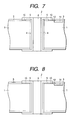
- FIG. 7 illustrates a substrate 1, a through hole 2, a protective layer 3, an insulating layer 4, an electroconductive layer 5, a filling material 6, an electrode pad 10, a semiconductor element 11, and a wiring conductor 12.
- the insulating layer 4 is formed on the inside surface of the through hole 2 and on the front and back surfaces of the substrate 1 around the opening ends of the through hole 2. In this embodiment, the insulating layer 4 is formed only on the inside surface of the through hole 2.
- the insulating layer 4 in this embodiment is formed in such a manner that a masking insulating film is formed on the protective layer 3 before the insulating layer 4 is formed, and the masking insulating film is peeled off after the formation of the insulating layer 4.
- the methods of forming the members other than the insulating layer 4 in this embodiment are the same as those in Embodiment 1.
- the insulating layer 4 is formed only on the inside surface of the through hole 2, so that the thickness around the opening ends of the through hole can be reduced to reduce the overall thickness of the semiconductor device.
- FIG. 8 illustrates a substrate 1, a through hole 2, a protective layer 3, an insulating layer 4, an electroconductive layer 5, a filling material 6, an electrode pad 10, a semiconductor element 11, and a wiring conductor 12.
- the electrode pad 10 is formed as a circular ring surrounding the opening end of the through hole 2.
- the electrode pad 10 is formed in contact with the opening end of the through hole 2 with no given spacing from the opening end.
- the method of forming the semiconductor device in this embodiment is the same as that in the Embodiment 1.
- the thickness of the protective layer is 0.1 to 6 ⁇ m and the thickness of the electrode pad is 0.02 to 5 ⁇ m. Therefore the thickness in the vicinity of the opening end of the through hole 2 can be further reduced by an amount corresponding to the difference in thickness.
- FIG. 9 illustrates a substrate 1, a through hole 2, a protective layer 3, an insulating layer 4, an electroconductive layer 5, a filling material 6, an electrode pad 10, a semiconductor element 11, and a wiring conductor 12.
- the electrode pad 10 is formed as a circular ring surrounding the opening end of the through hole 2.
- the electrode pad 10 is rectangular and is placed by the side of the through hole 2 without surrounding the through hole 2.
- the electroconductive layer 5 is formed only in one direction from the through hole to a region where the electrode pad 10 is formed.
- the vacant space around the portion provided in the vicinity of the opening end of the through hole 2 for conduction between the front and back surfaces of the substrate is increased, so that the regions on the front and back surfaces of the substrate can be effectively utilized to enable packaging at a higher density.
- FIG. 10 illustrates a substrate 1, a through hole 2, a protective layer 3, an insulating layer 4, an electroconductive layer 5, a filling material 6, a semiconductor element 11, and a wiring conductor 12.
- the electrode pad 10 is used as an electrical connection portion.
- the wiring conductor 12 is exposed out of the protective layer 3 to be directly connected to the electroconductive layer 5. Since there is no need to form an electrode pad, the manufacturing cost of the semiconductor device can be reduced.
- FIG. 11 illustrates a substrate 1, a through hole 2, a protective f layer 3, an insulating layer 4, an electroconductive layer 5, a filling material 6, electrode pads 10, semiconductor elements 11, and wiring conductors 12.
- the electrode pad 10, the semiconductor element 11 and the wiring conductor 12 are formed on the back surface of the substrate 1, as well as on the front surface, and the semiconductor element 11 on the front surface of the substrate 1 and the semiconductor element 11 on the back surface are electrically connected to each other via the wiring conductors 12, the electrode pads 10 and the electroconductive layer 5.
- the back surface of the substrate 1 can also be used as a surface for forming semiconductor elements, so that the regions on the front and back surfaces of the substrate can be effectively utilized to enable packaging at a higher density.
- FIGS. 12 and 13 illustrate a substrate 1, a protective layer 3, an insulating layer 4, an electroconductive layer 5, a filling material 6, an electrode pad 10, a semiconductor element 11, and a wiring conductor 12.
- the insulating layer 4 and the electroconductive layer 5 are formed on the inside surface of the through hole 2 for conduction between the front and back surfaces of the substrate 1.
- a groove 13 is formed in a side surface the substrate 1, and the insulating layer 4 and the electroconductive layer 5 are formed on the inside surface of the groove 13.
- the substrate 1 is cut at the positions corresponding to the center axes (indicated by arrow D) of the through holes 2 as shown in FIG. 14 instead of being cut at the positions indicated by arrow C in the step shown in FIG. 3G in Embodiment 1.
- a semiconductor device in which the insulating layer 4 and the electroconductive layer 5 are formed in the side surface of the substrate 1 is thereby fabricated.
- the region located in an outward direction from each through hole 2 in each of Embodiments 1 to 6 can be removed to reduce the width of one semiconductor device (the lateral direction in FIG. 14). Therefore the size of a unit in which the semiconductor device is mounted can be made compact. Also, the number of semiconductor devices formable from one wafer can be increased to reduce the manufacturing cost.
- a semiconductor device and a method of manufacturing the semiconductor device in which an electrical connection is established between the front and back surfaces of a substrate via at least one through hole formed through the substrate between the front and back surfaces; an electrical connection portion is formed on at least one surface of the front and back surfaces of the substrate in the vicinity of the opening ends of the through hole by a semiconductor process; an insulating layer formed of an organic material is formed on the inside surface of the through hole; an electroconductive layer is formed on the inside surface of the insulating layer; and the electrical connection portion is electrically connected to the electroconductive layer to be electrically connected to a side of the other surface of the substrate.
- an improved semiconductor device can be provided in which reliable electrical conduction is provided between the front and back surfaces of the substrate.
- the insulating layer is composed of an organic material, particularly a binder resin to be cured at a temperature not higher than 400°C. Therefore the insulating layer can be formed by a liquid phase method.
- the binder resin is one selected from the group consisting of a denatured epoxy resin, a polyamide resin, a polyimide resin, a maleimide resin, a polyimide-amide resin, a polyester resin, a polyether resin, a bisphenol resin, a denatured acrylic resin, a silicone resin, a fluorocarbon resin, and a melamine resin, or a resin mixture obtained by suitably combining these resins.
- This resin is cured with one of polymerization reaction-generated bonding, condensation reaction-generated bonding, addition reaction-generated bonding, urethane bonding, urea bonding, ester bonding, ether bonding, carbonate bonding, thiourethane bonding, thioester bonding, thioether bonding, amide bonding, unsaturated bonding, and siloxane bonding.
- the process of forming the through hole includes no process at a high temperature of 600°C or higher, such as thermal oxidation processing or chemical vapor deposition. Therefore it is possible to form the through hole on the substrate on which the semiconductor element and the electrical connection portion connecting to the semiconductor element are formed in advance, and to thereby provide conduction between the front and back surfaces of the substrate. Thus, the manufacturing process can be simplified and the manufacturing cost can be reduced.
- the through hole perpendicular to the surface of the substrate can be easily formed by laser machining. Therefore the spaces on the front and back surfaces of the substrate 1 can be effectively utilized.
- the insulating layer is formed by electrodeposition to be formed only on the inside surface of the through hole without using a mask or the like. Since the uniformity of the film is markedly high, the insulating layer can be formed with uniformity on the inside surface of the through hole even when the aspect ratio of the through hole is 5 or higher or the inside diameter of the through hole is 100 ⁇ m or smaller. Therefore no defect occurs in the insulating layer. For this reason, there is substantially no possibility of occurrence of leakage between the electroconductive substrate and the electroconductive layer formed on the inside surface of the insulating layer, which may result in device failure, and the semiconductor device can be formed with improved reliability.
- the electroconductive layer is formed by electroless plating. Therefore a uniform electroconductive film can be easily formed even on the surface of the insulating layer in a short time.
- the electrical connection portion is formed in the shape of a circular ring so as to encircle the opening end of the through hole, so that a reliable connection can be established between the electrical connection portion and the electroconductive layer.
- the space inside the electroconductive layer formed in the through hole is filled with a filling material to prevent degradation of the electroconductive layer and the insulating layer with the elapse of time due to contamination of foreign materials or due to contact with external air for example, thereby further improving the reliability of the semiconductor substrate.
- An insulating material may be used as the filling material. In such a case, even if the filling material is attached to the surface of the substrate in the filling step, it does not cause a short circuit of a conductor exposed in the surface of the substrate unlike a electroconductive filling material.
- the through hole may be filled with the filling material by the process including the step of putting the electroconductive substrate in a vacuum atmosphere, the step of filling at least part of the through hole with the filling material, and the step of pressurizing the filling material in the through hole.
- This process ensures that filling can be completed with no void left in the through hole. There is no possibility of a void expanding with increasing temperature to press the electroconductive layer and thereby cause variation in resistance value or a break in the electroconductive layer. Consequently, the reliability of the semiconductor device can be improved.
- the insulating layer may be formed only on the inside surface of the through hole. The thickness of the semiconductor substrate in the vicinity of the opening end of the through hole 2 is reduced in this way to reduce the overall thickness of the semiconductor device.
- the electrode pad may be formed in contact with the opening end of the through hole with no given spacing from the opening end.
- the protective layer in the vicinity of the opening end of the through hole is thereby omitted, so that the thickness of the substrate in the vicinity of the opening end of the through hole can be further reduced.
- the electrode pad may be placed by the side of the through hole without surrounding the through hole, and the electroconductive layer may be formed only in one direction on the side of the through hole where the electrode pad is formed.
- the vacant space around the portion provided in the vicinity of the opening end of the through hole is thereby increased, so that the regions on the front and back surfaces of the substrate can be effectively utilized to enable packaging at a higher density.
- the electrical connection may be formed by exposing the wiring conductor out of the protective layer and directly connecting the wiring conductor to the electroconductive layer. The need for forming the electrode pad is thereby eliminated to reduce the manufacturing cost of the semiconductor device.
- a semiconductor element formation surface may also be provided in the back surface of the substrate to enable efficient use of the regions on the front and back surfaces of the substrate and to enable packaging at a higher density.
- a method of manufacturing a semiconductor device in which a substrate having, on a front surface thereof, an electrical connection portion formed by a semiconductor process is prepared; at least one through hole is formed in the substrate at a predetermined position; an insulating layer formed of an organic material is formed on the inside surface; and an electroconductive layer electrically connected to the electrical connection portion is formed on the inside surface of the insulating layer to electrically connect the electrical connection portion to a side of the back surface of the substrate.
- the region located in an outward direction from the through hole can be removed in this way to reduce the width of one semiconductor device (the lateral direction in FIG. 13). Therefore the size of a unit in which the semiconductor device is mounted can be made compact. Also, the number of semiconductor devices formable from one wafer can be increased to reduce the manufacturing cost.
Landscapes
- Internal Circuitry In Semiconductor Integrated Circuit Devices (AREA)
Abstract
Description
| Number of cycles | 0 (Initial value) | 50 | 100 | 150 | 200 |
| Resistance value (Ω) | 65 | 66 | 65 | 66 | 66 |
| Test time (h) | 0 (Initial value) | 50 | 100 |
| Resistance value (Ω) | 5× | 5× | 3×10E12 |
| | 1 | 2 | 3 | 4 | 5 | 6 | 7 |
| Thickness of substrate (µm) | 625 | 300 | 300 | 500 | 625 | 625 | 100 |
| Inside diameter of through hole (µm) | 80 | 10 | 5 | 100 | 100 | 5 | 3 |
| Aspect ratio | 15.6 | 30 | 60 | 5.0 | 6.25 | 125 | 33.3 |
| Heat cycle test | ○ | ○ | ○ | ○ | ○ | ○ | × |
| Constant-temperature constant-humidity test | ○ | ○ | ○ | ○ | ○ | × | × |
| Final results | ○ | ○ | ○ | ○ | ○ | × | × |
| ○:Good; ×:Bad |
Claims (31)
- A semiconductor device in which an electrical connection is established between front and back surfaces of a substrate (1) by means of at least one through hole (2) formed through said substrate between the front and back surfaces, said semiconductor device being characterized in that:an electrical connection portion (10) is formed by a semiconductor process on at least one surface of the front and back surfaces of said substrate in a vicinity of an end opening of said through hole;an insulating layer (4) formed of an organic material is formed on at least an inside surface of said through hole;an electroconductive layer (5) is formed on at least an inside surface of said insulating layer; andsaid electrical connection portion is electrically connected to said electroconductive layer to be electrically connected to a side of the other surface of said substrate.
- The semiconductor device according to claim 1, characterized in that said organic material comprises a binder resin to be cured at a temperature equal to or lower than 400°C.
- The semiconductor device according to claim 2, characterized in that said binder resin is one selected from the group consisting of a denatured epoxy resin, a polyamide resin, a polyimide resin, a maleimide resin, a polyimide-amide resin, a polyester resin, a polyether resin, a bisphenol resin, a denatured acrylic resin, a silicone resin, a fluorocarbon resin, and a melamine resin, or a resin mixture obtained by suitably combining these resins, and is cured with one of polymerization reaction-generated bonding, condensation reaction-generated bonding, addition reaction-generated bonding, urethane bonding, urea bonding, ester bonding, ether bonding, carbonate bonding, thiourethane bonding, thioester bonding, thioether bonding, amide bonding, unsaturated bonding, and siloxane bonding.
- The semiconductor device according to claim 1, characterized in that said substrate is a semiconductor substrate.
- The semiconductor device according to claim 1, characterized in that an aspect ratio of said through hole is in a range from 5 to 60.
- The semiconductor device according to claim 1, characterized in that an inside diameter of said through hole is in a range from 5 µm to 100 µm.
- The semiconductor device according to claim 1, characterized in that said electrical connection portion is formed in a shape of a circular ring so as to encircle the opening end of said through hole.
- The semiconductor device according to claim 1, characterized in that said insulating layer is formed only on the inside surface of said through hole.
- The semiconductor device according to claim 1, characterized in that said electrical connection portion is adjacent to the opening end of said through hole.
- The semiconductor device according to claim 1, characterized in that said electrical connection portion is rectangular.
- The semiconductor device according to claim 1, characterized in that said electrical connection portion comprises wiring.
- The semiconductor device according to claim 1, characterized in that another electrical connection portion electrically connected to said electroconductive layer is also formed on the other surface of said substrate.
- The semiconductor device according to claim 1, characterized in that a space inside the electroconductive layer formed in said through hole is filled with a filling material.
- The semiconductor device according to claim 13, characterized in that said filling material is an insulating material.
- A semiconductor device in which an electrical connection is established between front and back surfaces of a substrate (1), said semiconductor device being characterized in that:at least one groove (13) connecting the front and back surfaces of said substrate is formed in a side surface of said substrate;an electrical connection portion (10) is formed by a semiconductor process on at least one surface of the front and back surfaces of said substrate in a vicinity of an end of said groove;an insulating layer (4) formed of an organic material is formed on at least an inside surface of said through hole;an electroconductive layer (5) is formed on at least an inside surface of said insulating layer; andsaid electrical connection portion is electrically connected to said electroconductive layer to be electrically connected to a side of the other surface of said substrate.
- The semiconductor device according to claim 15, characterized in that said organic material comprises a binder resin to be cured at a temperature equal to or lower than 400°C.
- The semiconductor device according to claim 16, characterized in that said binder resin is one selected from the group consisting of a denatured epoxy resin, a polyamide resin, a polyimide resin, a maleimide resin, a polyimide-amide resin, a polyester resin, a polyether resin, a bisphenol resin, a denatured acrylic resin, a silicone resin, a fluorocarbon resin, and a melamine resin, or a resin mixture obtained by suitably combining these resins, and is cured with one of polymerization reaction-generated bonding, condensation reaction-generated bonding, addition reaction-generated bonding, urethane bonding, urea bonding, ester bonding, ether bonding, carbonate bonding, thiourethane bonding, thioester bonding, thioether bonding, amide bonding, unsaturated bonding, and siloxane bonding.
- A method of manufacturing a semiconductor device in which an electrical connection is established between front and back surfaces of a substrate (1) by means of at least one through hole (2) formed through the substrate between the front and back surfaces of the substrate, said method being characterized in that:an electrical connection portion (10) is formed on at least one surface of the front and back surfaces of the substrate by a semiconductor process;at least one through hole (2) is formed in the substrate at a predetermined position;an insulating layer (4) formed of an organic material is formed on at least an inside surface of the through hole; andan electroconductive layer (5) electrically connected to the electrical connection portion is formed on at least an inside surface of the insulating layer to electrically connect the electrical connection portion to a side of the other surface of the substrate.
- The method according to claim 18, characterized in that the organic material comprises a binder resin to be cured at a temperature equal to or lower than 400°C.
- The method according to claim 18, characterized in that the binder resin is one selected from the group consisting of a denatured epoxy resin, a polyamide resin, a polyimide resin, a maleimide resin, a polyimide-amide resin, a polyester resin, a polyether resin, a bisphenol resin, a denatured acrylic resin, a silicone resin, a fluorocarbon resin, and a melamine resin, or a resin mixture obtained by suitably combining these resins, and is cured with one of polymerization reaction-generated bonding, condensation reaction-generated bonding, addition reaction-generated bonding, urethane bonding, urea bonding, ester bonding, ether bonding, carbonate bonding, thiourethane bonding, thioester bonding, thioether bonding, amide bonding, unsaturated bonding, and siloxane bonding.
- The method according to claim 18, characterized in that the substrate is a semiconductor substrate.
- The method according to claim 18, characterized in that the through hole is formed by laser machining.
- The method according to claim 18, characterized in that the insulating layer is formed by a liquid phase method using processing at a temperature equal to or lower than 400°C.
- The method according to claim 23, characterized in that the liquid phase method is electrodeposition method.
- The method according to claim 18, characterized in that the electroconductive layer is formed by electroless plating.
- The method according to claim 18, characterized in that a space inside the electroconductive layer in the through hole is filled with a filling material.
- The method according to claim 26, characterized in that the filling material is an insulating material.
- The method according to claim 27, characterized in that filling of the through hole with the filling material is performed by:a step of placing the substrate in a vacuum atmosphere;a step of closing one of opening ends of the through hole;a step of applying the filling material to a position corresponding to the other opening end in a surface level of the substrate; anda step of pressuring the filing material from the other opening end of the through hole.
- A method of manufacturing a semiconductor device in which an electrical connection is established between front and back surfaces of a substrate (1), said method being characterized in that:an electrical connection portion is formed on at least one surface of the front and back surface of the substrate by a semiconductor process;at least one through hole (2) is formed in the substrate at a predetermined position;an insulating layer (4) formed of an organic material is formed on at least an inside surface of the through hole;an electroconductive layer (5) electrically connected to the electrical connection portion is formed on at least an inside surface of the insulating layer to electrically connect the electrical connection portion to a side of the other surface of the substrate; andthe substrate is cut so that the through hole is bisected to form a groove (13) in a side surface of the cut substrate.
- The method according to claim 29, characterized in that the organic material comprises a binder resin to be cured at a temperature equal to or lower than 400°C.
- The method according to claim 29, characterized in that the binder resin is one selected from the group consisting of a denatured epoxy resin, a polyamide resin, a polyimide resin, a maleimide resin, a polyimide-amide resin, a polyester resin, a polyether resin, a bisphenol resin, a denatured acrylic resin, a silicone resin, a fluorocarbon resin, and a melamine resin, or a resin mixture obtained by suitably combining these resins, and is cured with one of polymerization reaction-generated bonding, condensation reaction-generated bonding, addition reaction-generated bonding, urethane bonding, urea bonding, ester bonding, ether bonding, carbonate bonding, thiourethane bonding, thioester bonding, thioether bonding, amide bonding, unsaturated bonding, and siloxane bonding.
Applications Claiming Priority (4)
| Application Number | Priority Date | Filing Date | Title |
|---|---|---|---|
| JP2002012834 | 2002-01-22 | ||
| JP2002012834 | 2002-01-22 | ||
| JP2002360904A JP2003289073A (en) | 2002-01-22 | 2002-12-12 | Semiconductor device and manufacturing method of semiconductor device |
| JP2002360904 | 2002-12-12 |
Publications (2)
| Publication Number | Publication Date |
|---|---|
| EP1329949A2 true EP1329949A2 (en) | 2003-07-23 |
| EP1329949A3 EP1329949A3 (en) | 2004-08-25 |
Family
ID=26625594
Family Applications (1)
| Application Number | Title | Priority Date | Filing Date |
|---|---|---|---|
| EP03001196A Withdrawn EP1329949A3 (en) | 2002-01-22 | 2003-01-21 | Semiconductor device and method of manufacturing semiconductor device |
Country Status (5)
| Country | Link |
|---|---|
| US (2) | US6856023B2 (en) |
| EP (1) | EP1329949A3 (en) |
| JP (1) | JP2003289073A (en) |
| KR (1) | KR20030063236A (en) |
| TW (1) | TW577132B (en) |
Cited By (4)
| Publication number | Priority date | Publication date | Assignee | Title |
|---|---|---|---|---|
| DE102006035865B3 (en) * | 2006-08-01 | 2008-03-06 | Infineon Technologies Ag | Material placing method for use in integrated circuit, involves positioning transfer plate opposite to target plate, where material is casted out from blind holes to contact with target plate and to place at target plate |
| EP2166036A4 (en) * | 2007-06-12 | 2011-10-19 | Sumitomo Bakelite Co | RESIN COMPOSITION, COATING MATERIAL, INSULATING LAYER AND SEMICONDUCTOR DEVICE |
| US8048479B2 (en) | 2006-08-01 | 2011-11-01 | Qimonda Ag | Method for placing material onto a target board by means of a transfer board |
| CN104668164A (en) * | 2015-03-19 | 2015-06-03 | 苏州光宝微电子科技有限公司 | UV-LED (Ultraviolet Light-emitting Diode) light source machine and light source machine curing control method |
Families Citing this family (89)
| Publication number | Priority date | Publication date | Assignee | Title |
|---|---|---|---|---|
| SG111069A1 (en) * | 2002-06-18 | 2005-05-30 | Micron Technology Inc | Semiconductor devices including peripherally located bond pads, assemblies, packages, and methods |
| SG107595A1 (en) * | 2002-06-18 | 2004-12-29 | Micron Technology Inc | Semiconductor devices and semiconductor device components with peripherally located, castellated contacts, assembles and packages including such semiconductor devices or packages and associated methods |
| KR100584965B1 (en) * | 2003-02-24 | 2006-05-29 | 삼성전기주식회사 | Package Substrate and Manufacturing Method Thereof |
| US20050046016A1 (en) * | 2003-09-03 | 2005-03-03 | Ken Gilleo | Electronic package with insert conductor array |
| US7345350B2 (en) * | 2003-09-23 | 2008-03-18 | Micron Technology, Inc. | Process and integration scheme for fabricating conductive components, through-vias and semiconductor components including conductive through-wafer vias |
| SG120123A1 (en) * | 2003-09-30 | 2006-03-28 | Micron Technology Inc | Castellated chip-scale packages and methods for fabricating the same |
| US7091124B2 (en) * | 2003-11-13 | 2006-08-15 | Micron Technology, Inc. | Methods for forming vias in microelectronic devices, and methods for packaging microelectronic devices |
| US8084866B2 (en) * | 2003-12-10 | 2011-12-27 | Micron Technology, Inc. | Microelectronic devices and methods for filling vias in microelectronic devices |
| JP2005268752A (en) * | 2004-02-19 | 2005-09-29 | Canon Inc | Laser cleaving method, member to be cleaved, and semiconductor element chip |
| JP4361826B2 (en) * | 2004-04-20 | 2009-11-11 | 新光電気工業株式会社 | Semiconductor device |
| US20050247894A1 (en) | 2004-05-05 | 2005-11-10 | Watkins Charles M | Systems and methods for forming apertures in microfeature workpieces |
| JP4430976B2 (en) * | 2004-05-10 | 2010-03-10 | 富士通株式会社 | Wiring board and manufacturing method thereof |
| US7232754B2 (en) * | 2004-06-29 | 2007-06-19 | Micron Technology, Inc. | Microelectronic devices and methods for forming interconnects in microelectronic devices |
| US7205486B2 (en) * | 2004-07-16 | 2007-04-17 | Cardiac Pacemakers, Inc. | Thermally isolated via structure |
| US7425499B2 (en) * | 2004-08-24 | 2008-09-16 | Micron Technology, Inc. | Methods for forming interconnects in vias and microelectronic workpieces including such interconnects |
| US20060043534A1 (en) * | 2004-08-26 | 2006-03-02 | Kirby Kyle K | Microfeature dies with porous regions, and associated methods and systems |
| SG120200A1 (en) * | 2004-08-27 | 2006-03-28 | Micron Technology Inc | Slanted vias for electrical circuits on circuit boards and other substrates |
| US7300857B2 (en) * | 2004-09-02 | 2007-11-27 | Micron Technology, Inc. | Through-wafer interconnects for photoimager and memory wafers |
| CN100481402C (en) * | 2004-09-10 | 2009-04-22 | 株式会社东芝 | Semiconductor device and manufacturing method thereof |
| JP4139803B2 (en) | 2004-09-28 | 2008-08-27 | シャープ株式会社 | Manufacturing method of semiconductor device |
| JP4246132B2 (en) * | 2004-10-04 | 2009-04-02 | シャープ株式会社 | Semiconductor device and manufacturing method thereof |
| JP4747707B2 (en) * | 2004-11-09 | 2011-08-17 | ソニー株式会社 | Multilayer wiring board and board manufacturing method |
| JPWO2006070652A1 (en) * | 2004-12-27 | 2008-06-12 | 日本電気株式会社 | Semiconductor device and manufacturing method thereof, wiring board and manufacturing method thereof, semiconductor package and electronic device |
| US7271482B2 (en) | 2004-12-30 | 2007-09-18 | Micron Technology, Inc. | Methods for forming interconnects in microelectronic workpieces and microelectronic workpieces formed using such methods |
| KR100946878B1 (en) * | 2005-01-10 | 2010-03-09 | 삼성전자주식회사 | Channel quality information channel allocation system and method in communication system |
| US20060177999A1 (en) * | 2005-02-10 | 2006-08-10 | Micron Technology, Inc. | Microelectronic workpieces and methods for forming interconnects in microelectronic workpieces |
| DE102005006995B4 (en) * | 2005-02-15 | 2008-01-24 | Infineon Technologies Ag | Semiconductor device with plastic housing and external connections and method for producing the same |
| US8278738B2 (en) * | 2005-02-17 | 2012-10-02 | Sharp Kabushiki Kaisha | Method of producing semiconductor device and semiconductor device |
| JP2006261323A (en) * | 2005-03-16 | 2006-09-28 | Sharp Corp | Semiconductor device and manufacturing method thereof |
| JP2006315017A (en) * | 2005-05-11 | 2006-11-24 | Canon Inc | Laser cutting method and member to be cut |
| US7402515B2 (en) * | 2005-06-28 | 2008-07-22 | Intel Corporation | Method of forming through-silicon vias with stress buffer collars and resulting devices |
| US7795134B2 (en) | 2005-06-28 | 2010-09-14 | Micron Technology, Inc. | Conductive interconnect structures and formation methods using supercritical fluids |
| US7863188B2 (en) * | 2005-07-29 | 2011-01-04 | Semiconductor Energy Laboratory Co., Ltd. | Semiconductor device and manufacturing method thereof |
| JP5357543B2 (en) * | 2005-08-26 | 2013-12-04 | コーニンクレッカ フィリップス エヌ ヴェ | Electrically shielded through-wafer interconnect |
| JP4828182B2 (en) * | 2005-08-31 | 2011-11-30 | 新光電気工業株式会社 | Manufacturing method of semiconductor device |
| US7863187B2 (en) | 2005-09-01 | 2011-01-04 | Micron Technology, Inc. | Microfeature workpieces and methods for forming interconnects in microfeature workpieces |
| US7622377B2 (en) * | 2005-09-01 | 2009-11-24 | Micron Technology, Inc. | Microfeature workpiece substrates having through-substrate vias, and associated methods of formation |
| US7262134B2 (en) | 2005-09-01 | 2007-08-28 | Micron Technology, Inc. | Microfeature workpieces and methods for forming interconnects in microfeature workpieces |
| US7723842B2 (en) * | 2005-09-02 | 2010-05-25 | Semiconductor Energy Laboratory Co., Ltd | Integrated circuit device |
| US7552534B2 (en) * | 2006-05-11 | 2009-06-30 | Eastman Kodak Company | Method of manufacturing an integrated orifice plate and electroformed charge plate |
| US7749899B2 (en) | 2006-06-01 | 2010-07-06 | Micron Technology, Inc. | Microelectronic workpieces and methods and systems for forming interconnects in microelectronic workpieces |
| FR2901635A1 (en) * | 2006-06-09 | 2007-11-30 | Commissariat Energie Atomique | DEVICE FOR THREE-DIMENSIONAL CONNECTION IN A SUBSTRATE |
| US7626269B2 (en) * | 2006-07-06 | 2009-12-01 | Micron Technology, Inc. | Semiconductor constructions and assemblies, and electronic systems |
| US7629249B2 (en) | 2006-08-28 | 2009-12-08 | Micron Technology, Inc. | Microfeature workpieces having conductive interconnect structures formed by chemically reactive processes, and associated systems and methods |
| US7902643B2 (en) | 2006-08-31 | 2011-03-08 | Micron Technology, Inc. | Microfeature workpieces having interconnects and conductive backplanes, and associated systems and methods |
| US7863189B2 (en) * | 2007-01-05 | 2011-01-04 | International Business Machines Corporation | Methods for fabricating silicon carriers with conductive through-vias with low stress and low defect density |
| US7829998B2 (en) * | 2007-05-04 | 2010-11-09 | Stats Chippac, Ltd. | Semiconductor wafer having through-hole vias on saw streets with backside redistribution layer |
| US7723159B2 (en) * | 2007-05-04 | 2010-05-25 | Stats Chippac, Ltd. | Package-on-package using through-hole via die on saw streets |
| US8445325B2 (en) | 2007-05-04 | 2013-05-21 | Stats Chippac, Ltd. | Package-in-package using through-hole via die on saw streets |
| EP1998371A1 (en) * | 2007-05-31 | 2008-12-03 | Infineon Technologies SensoNor AS | Method of manufacturing electrical conductors for a semiconductor device |
| JP2008305938A (en) * | 2007-06-07 | 2008-12-18 | Toshiba Corp | Semiconductor device, and manufacturing method thereof |
| JP5302522B2 (en) * | 2007-07-02 | 2013-10-02 | スパンション エルエルシー | Semiconductor device and manufacturing method thereof |
| SG150410A1 (en) | 2007-08-31 | 2009-03-30 | Micron Technology Inc | Partitioned through-layer via and associated systems and methods |
| DE102007051800A1 (en) * | 2007-10-26 | 2009-05-07 | Jenoptik Laserdiode Gmbh | Carrier body for semiconductor devices |
| KR101374338B1 (en) * | 2007-11-14 | 2014-03-14 | 삼성전자주식회사 | semicondoctor device having through-via and method of forming the same |
| US7884015B2 (en) | 2007-12-06 | 2011-02-08 | Micron Technology, Inc. | Methods for forming interconnects in microelectronic workpieces and microelectronic workpieces formed using such methods |
| JP4825784B2 (en) * | 2007-12-13 | 2011-11-30 | 新光電気工業株式会社 | Package for semiconductor device and method for manufacturing the same |
| JP5424675B2 (en) * | 2008-03-18 | 2014-02-26 | キヤノン株式会社 | Semiconductor device manufacturing method and semiconductor device |
| US7838967B2 (en) * | 2008-04-24 | 2010-11-23 | Powertech Technology Inc. | Semiconductor chip having TSV (through silicon via) and stacked assembly including the chips |
| TWI389291B (en) * | 2008-05-13 | 2013-03-11 | 財團法人工業技術研究院 | Three-dimensional stacked die package structure |
| US7872332B2 (en) | 2008-09-11 | 2011-01-18 | Micron Technology, Inc. | Interconnect structures for stacked dies, including penetrating structures for through-silicon vias, and associated systems and methods |
| JP5455538B2 (en) * | 2008-10-21 | 2014-03-26 | キヤノン株式会社 | Semiconductor device and manufacturing method thereof |
| KR20100048610A (en) | 2008-10-31 | 2010-05-11 | 삼성전자주식회사 | Semiconductor fackage and forming method of the same |
| JP5596919B2 (en) * | 2008-11-26 | 2014-09-24 | キヤノン株式会社 | Manufacturing method of semiconductor device |
| US8399354B2 (en) | 2009-01-13 | 2013-03-19 | Taiwan Semiconductor Manufacturing Company, Ltd. | Through-silicon via with low-K dielectric liner |
| JP5330863B2 (en) * | 2009-03-04 | 2013-10-30 | パナソニック株式会社 | Manufacturing method of semiconductor device |
| WO2011033516A1 (en) * | 2009-09-20 | 2011-03-24 | Viagan Ltd. | Wafer level packaging of electronic devices |
| JP5218497B2 (en) * | 2009-12-04 | 2013-06-26 | 株式会社デンソー | Semiconductor device and manufacturing method thereof |
| US9275934B2 (en) * | 2010-03-03 | 2016-03-01 | Georgia Tech Research Corporation | Through-package-via (TPV) structures on inorganic interposer and methods for fabricating same |
| TW201145493A (en) * | 2010-06-01 | 2011-12-16 | Chipmos Technologies Inc | Silicon wafer structure and multi-chip stack structure |
| CN102290397A (en) * | 2010-06-17 | 2011-12-21 | 南茂科技股份有限公司 | Silicon wafer structure and multi-die stack structure |
| JP5330323B2 (en) * | 2010-06-25 | 2013-10-30 | 有限会社 ナプラ | Insulator filling method for micro space |
| TWI400783B (en) * | 2010-07-21 | 2013-07-01 | 日月光半導體製造股份有限公司 | Package structure and manufacturing method thereof |
| US8519542B2 (en) * | 2010-08-03 | 2013-08-27 | Xilinx, Inc. | Air through-silicon via structure |
| JP5763775B2 (en) * | 2010-11-02 | 2015-08-12 | エンパイア テクノロジー ディベロップメント エルエルシー | Semiconductor structure with insulated through silicon vias |
| CN102468374A (en) | 2010-11-11 | 2012-05-23 | 展晶科技(深圳)有限公司 | Light-emitting diode manufacturing method |
| TWI425681B (en) * | 2010-11-15 | 2014-02-01 | Advanced Optoelectronic Tech | Method for manufacturing led |
| JP5313294B2 (en) * | 2011-05-16 | 2013-10-09 | 新光電気工業株式会社 | Semiconductor device |
| JP5820673B2 (en) * | 2011-09-15 | 2015-11-24 | 新光電気工業株式会社 | Semiconductor device and manufacturing method thereof |
| US9706667B2 (en) * | 2014-05-19 | 2017-07-11 | Sierra Circuits, Inc. | Via in a printed circuit board |
| KR101795480B1 (en) * | 2015-04-06 | 2017-11-10 | 코닝정밀소재 주식회사 | Substrate for ic package |
| JP6369436B2 (en) * | 2015-09-29 | 2018-08-08 | 大日本印刷株式会社 | Penetration electrode substrate and method of manufacturing the penetration electrode substrate |
| KR102504238B1 (en) * | 2016-03-08 | 2023-03-02 | 주식회사 아모센스 | Plugging Method for Via Hall of Ceramic Board |
| US10490348B2 (en) * | 2016-06-24 | 2019-11-26 | Qualcomm Incorporated | Two-dimensional structure to form an embedded three-dimensional structure |
| US10998221B2 (en) * | 2017-07-14 | 2021-05-04 | Micron Technology, Inc. | Semiconductor constructions having fluorocarbon material |
| JP6669201B2 (en) * | 2018-07-06 | 2020-03-18 | 大日本印刷株式会社 | Through-electrode substrate |
| US11342256B2 (en) * | 2019-01-24 | 2022-05-24 | Applied Materials, Inc. | Method of fine redistribution interconnect formation for advanced packaging applications |
| JP7014241B2 (en) * | 2020-02-25 | 2022-02-01 | 大日本印刷株式会社 | Manufacturing method of through silicon via board |
| TWI808716B (en) * | 2022-04-08 | 2023-07-11 | 欣興電子股份有限公司 | Circuit board and circuit board module with docking structure and manufacture method of the circuit board |
Family Cites Families (12)
| Publication number | Priority date | Publication date | Assignee | Title |
|---|---|---|---|---|
| US4601916A (en) * | 1984-07-18 | 1986-07-22 | Kollmorgen Technologies Corporation | Process for bonding metals to electrophoretically deposited resin coatings |
| JP2847890B2 (en) | 1990-04-27 | 1999-01-20 | 株式会社島津製作所 | Method of manufacturing semiconductor substrate for three-dimensional mounting |
| US5421083A (en) * | 1994-04-01 | 1995-06-06 | Motorola, Inc. | Method of manufacturing a circuit carrying substrate having coaxial via holes |
| JPH0992675A (en) | 1995-09-27 | 1997-04-04 | Olympus Optical Co Ltd | Semiconductor device and manufacturing method thereof |
| US6089442A (en) * | 1996-04-10 | 2000-07-18 | Canon Kabushiki Kaisha | Electrode connection method |
| US5910687A (en) * | 1997-01-24 | 1999-06-08 | Chipscale, Inc. | Wafer fabrication of die-bottom contacts for electronic devices |
| FR2767223B1 (en) | 1997-08-06 | 1999-09-17 | Commissariat Energie Atomique | INTERCONNECTION METHOD THROUGH SEMICONDUCTOR MATERIAL, AND DEVICE OBTAINED |
| US6180261B1 (en) * | 1997-10-21 | 2001-01-30 | Nitto Denko Corporation | Low thermal expansion circuit board and multilayer wiring circuit board |
| US6159754A (en) * | 1998-05-07 | 2000-12-12 | Intel Corporation | Method of making a circuit edit interconnect structure through the backside of an integrated circuit die |
| JP3813402B2 (en) * | 2000-01-31 | 2006-08-23 | 新光電気工業株式会社 | Manufacturing method of semiconductor device |
| JP3879816B2 (en) * | 2000-06-02 | 2007-02-14 | セイコーエプソン株式会社 | SEMICONDUCTOR DEVICE AND ITS MANUFACTURING METHOD, LAMINATED SEMICONDUCTOR DEVICE, CIRCUIT BOARD AND ELECTRONIC DEVICE |
| US6605551B2 (en) * | 2000-12-08 | 2003-08-12 | Intel Corporation | Electrocoating process to form a dielectric layer in an organic substrate to reduce loop inductance |
-
2002
- 2002-12-12 JP JP2002360904A patent/JP2003289073A/en not_active Withdrawn
-
2003
- 2003-01-21 EP EP03001196A patent/EP1329949A3/en not_active Withdrawn
- 2003-01-21 TW TW092101263A patent/TW577132B/en not_active IP Right Cessation
- 2003-01-22 KR KR10-2003-0004220A patent/KR20030063236A/en not_active Ceased
- 2003-01-22 US US10/347,937 patent/US6856023B2/en not_active Expired - Fee Related
-
2004
- 2004-10-15 US US10/964,714 patent/US7125810B2/en not_active Expired - Fee Related
Cited By (5)
| Publication number | Priority date | Publication date | Assignee | Title |
|---|---|---|---|---|
| DE102006035865B3 (en) * | 2006-08-01 | 2008-03-06 | Infineon Technologies Ag | Material placing method for use in integrated circuit, involves positioning transfer plate opposite to target plate, where material is casted out from blind holes to contact with target plate and to place at target plate |
| US8048479B2 (en) | 2006-08-01 | 2011-11-01 | Qimonda Ag | Method for placing material onto a target board by means of a transfer board |
| EP2166036A4 (en) * | 2007-06-12 | 2011-10-19 | Sumitomo Bakelite Co | RESIN COMPOSITION, COATING MATERIAL, INSULATING LAYER AND SEMICONDUCTOR DEVICE |
| EP2477215A3 (en) * | 2007-06-12 | 2013-08-14 | Sumitomo Bakelite Company Limited | Resin composition, embedding material, insulating layer and semiconductor device |
| CN104668164A (en) * | 2015-03-19 | 2015-06-03 | 苏州光宝微电子科技有限公司 | UV-LED (Ultraviolet Light-emitting Diode) light source machine and light source machine curing control method |
Also Published As
| Publication number | Publication date |
|---|---|
| US6856023B2 (en) | 2005-02-15 |
| US20050067713A1 (en) | 2005-03-31 |
| JP2003289073A (en) | 2003-10-10 |
| US20030151144A1 (en) | 2003-08-14 |
| TW200302527A (en) | 2003-08-01 |
| KR20030063236A (en) | 2003-07-28 |
| US7125810B2 (en) | 2006-10-24 |
| EP1329949A3 (en) | 2004-08-25 |
| TW577132B (en) | 2004-02-21 |
Similar Documents
| Publication | Publication Date | Title |
|---|---|---|
| US6856023B2 (en) | Semiconductor device and method of manufacturing semiconductor device | |
| US5904499A (en) | Package for power semiconductor chips | |
| US7034401B2 (en) | Packaging substrates for integrated circuits and soldering methods | |
| US5925931A (en) | Semiconductor device having interconnect lines and connection electrodes formed in groove portions of an insulating layer | |
| US6535398B1 (en) | Multichip module substrates with buried discrete capacitors and components and methods for making | |
| US6922339B2 (en) | Heat dissipating structure of printed circuit board and fabricating method thereof | |
| US5793105A (en) | Inverted chip bonded with high packaging efficiency | |
| KR100432715B1 (en) | Manufacturing method of PCB, PCB and package thereby | |
| US8895871B2 (en) | Circuit board having a plurality of circuit board layers arranged one over the other having bare die mounting for use as a gearbox controller | |
| KR20050008840A (en) | Methods for manufacturing electronic component and semiconductor device, semiconductor device, circuit board and electronic equipment | |
| US9502344B2 (en) | Wafer level packaging of electronic device | |
| JPH06350234A (en) | Method for attaching and contacting electrical and / or electronic components to an insulating substrate, method for manufacturing printed wiring board by currentless metal deposition, and method for attaching and contacting electronic components | |
| US6432748B1 (en) | Substrate structure for semiconductor package and manufacturing method thereof | |
| JP2006012895A (en) | Semiconductor device and manufacturing method of semiconductor device | |
| JP4352076B2 (en) | Semiconductor device heat dissipation structure | |
| RU2193259C1 (en) | Method for manufacturing three-dimensional polymeric electronic module | |
| JP2005332936A (en) | Semiconductor device and manufacturing method of semiconductor device | |
| JP4574025B2 (en) | Wiring module | |
| EP0117211B1 (en) | Method for fabricating a package for an integrated circuit | |
| JP4493563B2 (en) | Mounting structure of semiconductor device | |
| Tudanca et al. | A low cost manufacturing process for high density hybrid components based on multilayer polyimide/ceramic structures | |
| EP4614559A1 (en) | Circuit board and electronic module | |
| US20070123066A1 (en) | Interconnection element for BGA housings and method for producing the same | |
| EP0762494B1 (en) | Silicon semiconductor diode, its circuit module and structure with an insulation body and preparation method thereof | |
| JP4282711B2 (en) | Manufacturing method of heat dissipation structure |
Legal Events
| Date | Code | Title | Description |
|---|---|---|---|
| PUAI | Public reference made under article 153(3) epc to a published international application that has entered the european phase |
Free format text: ORIGINAL CODE: 0009012 |
|
| AK | Designated contracting states |
Designated state(s): AT BE BG CH CY CZ DE DK EE ES FI FR GB GR HU IE IT LI LU MC NL PT SE SI SK TR |
|
| AX | Request for extension of the european patent |
Extension state: AL LT LV MK RO |
|
| PUAL | Search report despatched |
Free format text: ORIGINAL CODE: 0009013 |
|
| AK | Designated contracting states |
Kind code of ref document: A3 Designated state(s): AT BE BG CH CY CZ DE DK EE ES FI FR GB GR HU IE IT LI LU MC NL PT SE SI SK TR |
|
| AX | Request for extension of the european patent |
Extension state: AL LT LV MK RO |
|
| 17P | Request for examination filed |
Effective date: 20050225 |
|
| AKX | Designation fees paid |
Designated state(s): DE FR GB IT NL |
|
| RBV | Designated contracting states (corrected) |
Designated state(s): DE FR GB IT NL |
|
| 17Q | First examination report despatched |
Effective date: 20071128 |
|
| STAA | Information on the status of an ep patent application or granted ep patent |
Free format text: STATUS: THE APPLICATION HAS BEEN WITHDRAWN |
|
| 18W | Application withdrawn |
Effective date: 20130328 |