EP1329928A2 - Electron-emitting element and field emission display using the same - Google Patents
Electron-emitting element and field emission display using the same Download PDFInfo
- Publication number
- EP1329928A2 EP1329928A2 EP02258747A EP02258747A EP1329928A2 EP 1329928 A2 EP1329928 A2 EP 1329928A2 EP 02258747 A EP02258747 A EP 02258747A EP 02258747 A EP02258747 A EP 02258747A EP 1329928 A2 EP1329928 A2 EP 1329928A2
- Authority
- EP
- European Patent Office
- Prior art keywords
- electron
- electrode
- emitting element
- electric field
- element according
- Prior art date
- Legal status (The legal status is an assumption and is not a legal conclusion. Google has not performed a legal analysis and makes no representation as to the accuracy of the status listed.)
- Withdrawn
Links
Images









Classifications
-
- H—ELECTRICITY
- H01—ELECTRIC ELEMENTS
- H01J—ELECTRIC DISCHARGE TUBES OR DISCHARGE LAMPS
- H01J1/00—Details of electrodes, of magnetic control means, of screens, or of the mounting or spacing thereof, common to two or more basic types of discharge tubes or lamps
- H01J1/02—Main electrodes
- H01J1/30—Cold cathodes, e.g. field-emissive cathode
- H01J1/316—Cold cathodes, e.g. field-emissive cathode having an electric field parallel to the surface, e.g. thin film cathodes
-
- G—PHYSICS
- G09—EDUCATION; CRYPTOGRAPHY; DISPLAY; ADVERTISING; SEALS
- G09G—ARRANGEMENTS OR CIRCUITS FOR CONTROL OF INDICATING DEVICES USING STATIC MEANS TO PRESENT VARIABLE INFORMATION
- G09G3/00—Control arrangements or circuits, of interest only in connection with visual indicators other than cathode-ray tubes
- G09G3/20—Control arrangements or circuits, of interest only in connection with visual indicators other than cathode-ray tubes for presentation of an assembly of a number of characters, e.g. a page, by composing the assembly by combination of individual elements arranged in a matrix no fixed position being assigned to or needed to be assigned to the individual characters or partial characters
- G09G3/22—Control arrangements or circuits, of interest only in connection with visual indicators other than cathode-ray tubes for presentation of an assembly of a number of characters, e.g. a page, by composing the assembly by combination of individual elements arranged in a matrix no fixed position being assigned to or needed to be assigned to the individual characters or partial characters using controlled light sources
-
- H—ELECTRICITY
- H01—ELECTRIC ELEMENTS
- H01J—ELECTRIC DISCHARGE TUBES OR DISCHARGE LAMPS
- H01J1/00—Details of electrodes, of magnetic control means, of screens, or of the mounting or spacing thereof, common to two or more basic types of discharge tubes or lamps
- H01J1/02—Main electrodes
- H01J1/30—Cold cathodes, e.g. field-emissive cathode
- H01J1/304—Field-emissive cathodes
-
- H—ELECTRICITY
- H01—ELECTRIC ELEMENTS
- H01J—ELECTRIC DISCHARGE TUBES OR DISCHARGE LAMPS
- H01J2201/00—Electrodes common to discharge tubes
- H01J2201/30—Cold cathodes
- H01J2201/306—Ferroelectric cathodes
-
- H—ELECTRICITY
- H01—ELECTRIC ELEMENTS
- H01J—ELECTRIC DISCHARGE TUBES OR DISCHARGE LAMPS
- H01J2201/00—Electrodes common to discharge tubes
- H01J2201/30—Cold cathodes
- H01J2201/316—Cold cathodes having an electric field parallel to the surface thereof, e.g. thin film cathodes
- H01J2201/3165—Surface conduction emission type cathodes
Definitions
- the present invention relates to an electron-emitting element and a field emission display using the same.
- Such an electron-emitting element has a driving electrode and an earth electrode, and is applied to various applications such as an field emission display (FED) and back light (for example, refer to Patent Literatures 1 to 5 and Non-Patent Literatures 1 to 3).
- FED field emission display
- back light for example, refer to Patent Literatures 1 to 5 and Non-Patent Literatures 1 to 3.
- a plurality of electron-emitting elements are two dimensionsally arranged in two dimensions and a plurality of phosphors being opposite to these electron-emitting elements are arranged at a certain space to each other.
- It is an object of the present invention is to provide an electron-emitting element having a good straight advancing ability of emitted electrons and a field emission display using the same.
- It is another object of the present invention is to provide an electron-emitting element realizing an electron emission with a high current density at a comparatively low vacuum and a remarkable low driving voltage and a field emission display using the same.
- an electron-emitting element comprising;
- electrons are emitted from the electric field applying portion by applying a pulse voltage to the first or second electrode.
- the electric field applying portion By composing the electric field applying portion by the dielectric, it is possible to obtain a good straight advancing ability that cannot be achieved by the conventional electron-emitting element. As a result, a voltage to be applied to the electron-emitting element needed to hold a desired current density is remarkably lower than that of the conventional electron-emitting element, and the energy consumption is greatly reduced. Since the first and second electrodes can be formed on the electric field applying portion by means of a thick film printing method, the electron-emitting element according to the present invention is preferable from the viewpoint of durability and cost reduction.
- a conductive coating portion to the first and second electrodes and the slit.
- the conductive coating portion there is remarkable reduction of the probability to damage the first and second electrodes caused by collision between electrons and ions or by generation of heat.
- the electron-emitting element further comprises a first conductive coating portion provided on the first electrode;
- a portion with a high resistance may be provided on the slit, the portion having a higher resistance than those of the first and the second conducting coating portions and being in contact with the first and the second conducting coating portions electrically.
- the portion with a high resistance has a higher voltage than those of the first and the second conductive coating portions when applying the voltage to the electron-emitting element, and thus the degree of the concentration of the electric field in the portion with a high resistance, or the slit is improved.
- a third electrode arranged at a certain space to the first and second electrodes, and to make the space between the first and second electrodes and the third electrode vacuum.
- Another electron-emitting element comprising:
- the electric field applying portion also acts as an actuator and may be bent and displaced when a pulse voltage is applied to the first or second electrode. As a result, the straight advancing ability of the electron-emitting element is more improved.
- the conductive coating portion In order to reduce the voltage to be applied to the electron-emitting element further more, it is preferable to apply the conductive coating portion to the first and second electrodes and the slit. In this case, by the application of the conductive coating portion, there is remarkable reduction of the probability to damage the first and second electrodes caused by collision between electrons and ions or by generation of heat.
- the electron-emitting element further comprises a first conductive coating portion provided on the first electrode;
- a portion with a high resistance may be provided on the slit, the portion having a higher resistance than those of the first and the second conducting coating portions and being in contact with the first and the second conducting coating portions electrically.
- the portion with a high resistance has a higher voltage than those of the first and the second conductive coating portions when applying the voltage to the electron-emitting element, and thus the degree of the concentration of the electric field in the portion with a high resistance, or the slit is improved.
- the electric field applying portion also acts as the actuator, and makes it possible to control the amount of emitted electrons by the displacement motion of the electric field applying portion.
- the electron-emitting element further has a voltage source for applying a direct offset voltage to the third electrode, and a resistor arranged in series between the voltage source and the third electrode.
- a desired current density can be easily achieved, and short-circuit between the third electrode and the first and second electrodes is prevented.
- a pulse voltage is applied to the first electrode, and a direct offset voltage is applied to the second electrode.
- the electron-emitting element further has a capacitor arranged in series between the first electrode and a voltage signal source.
- a voltage can be applied between the first electrode and the second electrode only until the capacitor is charged up, and as a result, the breakage caused by the short-circuit between the first and second electrodes is prevented.
- It may further have a resistor arranged in series between the second electrode and the direct offset voltage source.
- a resistor arranged in series between the second electrode and the direct offset voltage source.
- the relative dielectric constant of the electric field applying portion not less than 1000 and/or the width of said slit not more than 500 ⁇ m.
- At least one of the first and second electrodes prefferably have an angular part with an acute angle and/or for the first electrode and the second electrode to have carbon nanotubes, in other words, the particle or the flocculation body of the particles which includes carbon material having six-fold-ring structure.
- a field emission display according to the present invention is excellent in the straight advancing ability of the electron-emitting element, it is smaller in crosstalk in comparison with a display comprising conventional electron-emitting elements, the pitch between phosphors can be made more narrow, and it is not necessary to provide a grid in order to prevent electrons from striking on phosphors adjacent to the targeted phosphors. As a result, a field emission display according to the present invention is preferable from the viewpoint of improvement in resolution, downsizing and cost reduction of a display device.
- the emission of electrons can be performed even in case that the degree of vacuum inside a field emission display is comparatively low, it is possible to emit electrons even when the degree of vacuum inside the display is lowered by a cause such as a phosphor excitation and the like. Since a conventional field emission display needs to hold a comparatively large vacuum space as a margin for maintaining the emission of electrons, it has been difficult to make the display thin-sized. On the other hand, since the present invention does not need to hold a large vacuum space in advance in order to keep the emission of electrons against drop of the degree of vacuum, it is possible to make the display thin-sized.
- the conductive coating portion In order to reduce the voltage to be applied to the electron-emitting element further more, it is preferable to apply the conductive coating portion to the first and second electrodes and the slit. In this case, by the application of the conductive coating portion, there is remarkable reduction of the probability to damage the first and second electrodes caused by collision between electrons and ions or by generation of heat.
- the electron-emitting element further comprises a first conductive coating portion provided on the first electrode;
- a portion with a high resistance may be provided on the slit, the portion having a higher resistance than those of the first and the second conducting coating portions and being in contact with the first and the second conducting coating portions electrically.
- the portion with a high resistance has a higher voltage than those of the first and the second conductive coating portions when applying the voltage to the electron-emitting element, and thus the degree of the concentration of the electric field in the portion with a high resistance, or the slit is improved.
- a third electrode arranged at a certain space to the first and second electrodes and make the space between the first and second electrodes and the third electrode vacuum.
- a field emission display according to the present invention is excellent in the straight advancing ability of the electron-emitting element, it is more preferable from the viewpoint of miniaturizing and cost reduction of a display device.
- the conductive coating portion In order to reduce the voltage to be applied to the electron-emitting element furthermore, it is preferable to apply the conductive coating portion to the first and second electrodes and the slit. In this case, by the application of the conductive coating portion, there is remarkable reduction of the probability to damage the first and second electrodes caused by collision between electrons and ions or by generation of heat.
- the electron-emitting element further comprises a first conductive coating portion provided on the first electrode;
- a portion with a high resistance may be provided on the slit, the portion having a higher resistance than those of the first and the second conducting coating portions and being in contact with the first and the second conducting coating portions electrically.
- the portion with a high resistance has a higher voltage than those of the first and the second conductive coating portions when applying the voltage to the electron-emitting element, and thus the degree of the concentration of the electric field in the portion with a high resistance, or the slit is improved.
- the electric field applying portion also acts as an actuator and can control the amount of emitted electrons by the displacement motion of the electric field applying portion.
- the electron-emitting element further has a voltage source for applying a direct offset voltage to the third electrode and a resistor arranged in series between this voltage source and the third electrode.
- a desired current density namely, a desired amount of luminescence of phosphors can be easily achieved, and the short-circuit between the third electrode and the first and second electrodes is prevented.
- a pulse voltage is applied to the first electrode and a direct offset voltage is applied to the second electrode.
- the electron-emitting element further has a capacitor arranged in series between the first electrode and the voltage signal source. Thereby, the breakage to be caused by the short-circuit between the first and second electrodes is prevented.
- the electron-emitting element further has a fourth electrode formed on the other surface of the electric field applying portion and facing the first electrode, the breakage to be caused by the short-circuit between the first and second electrodes.
- a pulse voltage is applied to the fourth electrode and a direct offset voltage is applied to the second electrode.
- the electron-emitting element further has a resistor arranged in series between the second electrode and the direct offset voltage source, the breakage to be caused by the short-circuit between the first and second electrodes is prevented.
- the relative dielectric constant of the electric field applying portion not less than 1000 and/or the width of the slit not more than 500 ⁇ m.
- At least one of the first and second electrodes prefferably has an angular part with an acute angle and/or for the first and second electrodes to have carbon nanotubes.
- a field emission display further comprises a substrate having a plurality of electron-emitting elements arranged in two-dimensions and formed into one body with it.
- FIG 1A is a top view of a first embodiment of the electron-emitting element according to the present invention
- Figure 1B is a sectional view taken along line I-I.
- This electron-emitting element has an electric field applying portion 1 composed of a dielectric, a driving electrode 2 as a first electrode formed on one surface of the electric field applying portion 1 and a common electrode 3 as a second electrode formed on the surface on which the driving electrode 2 is formed and forming a slit in cooperation with the driving electrode 2, and the electron-emitting element is formed on a substrate 4.
- this electron-emitting element further has an electron capturing electrode 5 as a third electrode arranged at a certain space to the one surface of the electric field applying portion 1, and keeps the space therebetween in a vacuum state.
- an electron capturing electrode 5 as a third electrode arranged at a certain space to the one surface of the electric field applying portion 1, and keeps the space therebetween in a vacuum state.
- a capacitor not illustrated is arranged in series between the driving electrode 2 and an not shown voltage signal source and/or an not shown resistor is arranged in series between the common electrode 3 and an not shown direct offset voltage source.
- a dielectric being comparatively high, for example, not less than 1000 in relative dielectric constant is preferably adopted as a dielectric forming the electric field applying portion 1.
- a dielectric there can be mentioned ceramic containing barium titanate, lead zirconate, magnesium lead niobate, nickel lead niobate, zinc lead niobate, manganese lead niobate, magnesium lead tantalate, nickel lead tantalate, antimony lead stannate, lead titanate, barium titanate, magnesium lead tungstate, cobalt lead niobate or the like, or an optional combination of these, and ceramic containing these compounds of 50 wt% or more as its main ingredients, and furthermore ceramic having an oxide of lanthanum, calcium, strontium, molybdenum, tungsten, barium, niobium, zinc, manganese, nickel or the like, or some combination of these or other compounds and the like properly added to said ceramic.
- nPMN-mPT (n and m are represented in molar ratio) of magnesium lead niobate (PMN) and lead titanate (PT)
- PMN magnesium lead niobate
- PT lead titanate
- a three-component system of magnesium lead niobate (PMN), lead titanate (PT) and lead zirconate (PZ) it is preferable for the purpose of making the relative dielectric constant to make the composition of the three-component system close to the composition of the vicinity of the morphotropic phase boundary (MPB) between a tetragonal system and a pseudo-tetragonal system or between a tetragonal system and a rhombohedral system as a manner other than making the molar ratio of PMN be large.
- MPB morphotropic phase boundary
- the driving electrode 2 has an angular part with an acute angle.
- a pulse voltage is applied to the driving electrode 2 from an not shown power source, and electrons are emitted mainly from the angular part.
- the width ⁇ of the slit between the driving electrode 2 and the common electrode 3 is preferably not more than 500 ⁇ m.
- the driving electrode 2 is composed of a conductor with resistance to a high-temperature oxidizing atmosphere, for example, a single metal, an alloy, a mixture of an insulating ceramic and a single metal, a mixture of an insulating ceramic and an alloy or the like, and is preferably composed of a high-melting point precious metal such as platinum, palladium, rhodium, molybdenum or the like, or a material having such an alloy as silver-palladium, silver-platinum, platinum-palladium or the like as its main ingredient, or a cermet material of platinum and ceramic. More preferably, it is composed of only platinum or a material having a platinum-based alloy as its main ingredient.
- carbon-based or graphite-based materials for example, a diamond thin film, a diamond-like carbon and a carbon nanotube are also preferably used.
- a ceramic material added to the electrode material is preferably 5 to 30 vol%.
- the driving electrode 2 can be composed using the above-mentioned materials by an ordinary film forming method by means of various thick film forming methods such as screen printing, spraying, coating, dipping, application, electrophoresing and the like, or various thin film forming methods such as sputtering, ion beaming, vacuum deposition, ion plating, CVD, plating and the like, and is preferably made by these thick film forming methods.
- various thick film forming methods such as screen printing, spraying, coating, dipping, application, electrophoresing and the like
- various thin film forming methods such as sputtering, ion beaming, vacuum deposition, ion plating, CVD, plating and the like, and is preferably made by these thick film forming methods.
- a thickness of driving electrode 2 is generally not more than 20 ⁇ m, and preferably not more than 5 ⁇ m.
- a direct offset voltage is applied to the common electrode 3, and is led by the wiring passing through an not shown through hole from the reverse side of the substrate 4.
- the common electrode 3 is formed by means of a material and method similar to those for the driving electrode 2, and preferably by means of the above-mentioned thick film forming methods.
- the width of the common electrode 3 also is generally not more than 20 ⁇ m and preferably not more than 5 ⁇ m.
- the substrate 4 is composed of an electrically insulating material in order to electrically separate a wire electrically connected to the driving electrode 2 and a wire electrically connected to the common electrode 3 from each other.
- the substrate 4 can be composed of a material like an enameled material obtained by coating the surface of a high heat-resistant metal with a ceramic material such as glass and the like, and is optimally composed of ceramic.
- stabilized zirconium oxide aluminum oxide, magnesium oxide, titanium oxide, spinel, mullite, aluminum nitride, silicon nitride, glass, a mixture of these and the like can be used.
- aluminum oxide and stabilized zirconium oxide are preferable from the viewpoint of strength and rigidity.
- Stabilized zirconium oxide is particularly preferable in that it is comparatively high in mechanical strength, comparatively high in toughness and comparatively small in chemical reaction to the driving electrode 2 and the common electrode 3.
- the stabilized zirconium oxide includes stabilized zirconium oxide and partially stabilized zirconium oxide. Since the stabilized zirconium oxide takes a crystal structure such as a cubic system, it undergoes no phase transition.
- the stabilized zirconium oxide contains a stabilizer such as calcium oxide, magnesium oxide, yttrium oxide, scandium oxide, ytterbium oxide, cerium oxide, rare metal oxide and the like of 1 to 30 mol%. It is preferable for a stabilizer to contain yttrium oxide in order to improve the substrate 4 in mechanical strength. In this case, it contains yttrium of preferably 1.5 to 6 mol%, more preferably 2 to 4 mol%, and preferably further contains aluminum oxide of 1 to 5 mol%.
- crystal phase can be made into a mixed phase of "cubic system + monoclinic system", a mixed phase of "tetragonal system + monoclinic system”, a mixed phase of "cubic system + tetragonal system + monoclinic system” or the like, and among them particularly the crystal phase having a tetragonal system or a mixed phase of "tetragonal system + cubic system” as its main crystal phase is optimal from the viewpoint of strength, toughness and durability.
- the average particle diameter of the crystal particles is be preferably 0.05 to 2 ⁇ m, and more preferably 0.1 to 1 ⁇ m.
- the electric field applying portion 1, the driving electrode 2 and the common electrode 3 can be formed into one body together with the substrate 4 by applying heat treatment to the substrate 4, namely, by baking the substrate 4 each time forming one of them respectively, or these electric field applying portion 1, the driving electrode 2 and the common electrode 3 are formed on the substrate 4 and thereafter are heat-treated, namely, are baked at the same time and thereby they are formed into one body together with the substrate 4 at the same time.
- any heat treatment namely, baking for unification of them may not be needed.
- a heat treatment temperature namely, a baking temperature for forming the electric field applying portion 1, the driving electrode 2 and the common electrode 3 into one body together with the substrate 4 takes a temperature range of generally 500 to 1,400°C, and preferably 1,000 to 1,400°C.
- heat treatment namely, baking as controlling the vapor source and the atmosphere of the electric field applying portion 1
- a technique of baking as preventing the surface of the electric field applying portion 1 from being exposed directly to the baking atmosphere by covering the electric field applying portion 1 with a proper member.
- a material similar to the substrate 4 is used as the covering member.
- FIG 2A is a top view of a second embodiment of the electron-emitting element according to the present invention
- Figure 2B is a sectional view taken along a line II-II of it.
- This electron-emitting element has an electric field applying portion 11, a driving electrode 12 and a common electrode 13 respectively corresponding to the electric field applying portion 1, the driving electrode 2 and the common electrode 3, and additionally to them, further has a driving terminal electrode 14 as a fourth electrode formed on the other surface of the electric field applying portion 11, and they are formed on a substrate 15.
- the electron-emitting element further has an electron capturing electrode 16 as a third electrode being arranged at a certain space to one surface of the electric field applying portion 11, and keeps the space therebetween in a vacuum state.
- the electric field applying portion 11 between the driving electrode 12 and the driving terminal electrode 14 acts as a capacitor, it is not necessary to provide an additional capacitor in order to prevent breakage caused by short-circuit between the driving electrode 12 and the common electrode 13.
- a pulse voltage is applied to the driving terminal electrode 14 and a direct offset voltage is applied to the common electrode 13.
- the driving terminal electrode 14 is also formed by means of a similar material and technique to those for the driving electrode 12 and the common electrode 13, and preferably formed by means of one of the above-mentioned thick film forming methods.
- the thickness of the driving terminal electrode 14 is also generally not more than 20 ⁇ m, and preferably not more than 5 ⁇ m.
- Figure 3A is a top view of a third embodiment of the electron-emitting element according to the present invention
- Figure 3B is a sectional view taken along a line III-III of it.
- a driving electrode 22 and a common electrode 23 are formed on one surface of an electric field applying portion 21, and a plurality of carbon nanotubes (CNT) are provided on the surfaces of these driving electrode 22 and common electrode 23, and thereby it is easy to emit electrons from the top of the CNT when applying a pulse voltage to the driving electrode 22 and applying a direct offset voltage to the common electrode 23.
- CNT carbon nanotubes
- FIG 4A is a top view of a fourth embodiment of the electron-emitting element according to the present invention
- Figure 4B is a sectional view taken along a line IV-IV of it.
- a driving electrode 32 and a common electrode 33 are formed on one surface of an electric field applying portion 31, and a driving terminal electrode 34 is formed on the other surface of it, and a plurality of carbon nanotubes (CNT) are provided on the surfaces of these driving electrode 32 and common electrode 33, and thereby it is easy to emit electrons from the top of the CNT when applying a pulse voltage to the driving electrode 32 and applying a direct offset voltage to the common electrode 33.
- CNT carbon nanotubes
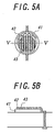
- Figure 5A is a top view of a fifth embodiment of the electron-emitting element according to the present invention
- Figure 5B is a sectional view taken along a line V-V of it.
- a driving electrode 42 and a common electrode 43 which are in the shape of the teeth of a comb are formed on one surface of an electric field applying portion 41. In this case, it is easy to emit electrons from the angular parts of these driving electrode 42 and common electrode 43.
- Figure 6A is a top view of a sixth embodiment of the electron-emitting element according to the present invention
- Figure 6B is a sectional view taken along a line VI-VI of it.
- the electron-emitting element has electric field applying portions 51a, 51b made of an antiferroelectric material, and driving electrodes 52a, 52b and common electrodes 53a, 53b which are in the shape of the teeth of a comb and are formed respectively on one-side surfaces of the electric field applying portions 51a, 51b.
- the electron-emitting element is disposed on a sheet layer 56 provided through a spacer layer 54 on a substrate 55.
- the electric field applying portions 51a, 51b, the driving electrodes 52a, 52b, the common electrodes 53a, 53b, the sheet layer 56 and the spacer layer 54 form actuators 57a, 57b, respectively.
- an antiferroelectric material for forming the electric field applying portions 51a, 51b it is preferable to use a material having lead zirconate as its main ingredient, a material having a component consisting of lead zirconate and lead stannate as its main ingredient, a material obtained by adding lanthanum oxide to lead zirconate, or a material obtained by adding lead zirconate or lead niobate to a component consisting of lead zirconate and lead stannate.
- an antiferroelectric material containing a component consisting of lead zirconate and lead stannate Its composition is as follows.
- the antiferroelectric materials can be also made porous, and in this case it is preferable to make the porosity be not more than 30%.
- the electric field applying portions 51a, 51b are preferably formed by means of one of the above-mentioned thick film forming methods, and a screen printing method is preferably in particular used by reason that it can perform inexpensively a fine printing.
- the thickness of the electric field applying portions 51a, 51b is made to be preferably 50 ⁇ m or less and more preferably 3 to 40 ⁇ m from the reason of obtaining a large displacement at a low operating voltage and the like.
- a film can be formed on the surface of the sheet layer 56 using paste or slurry having as its main ingredient antiferroelectric ceramic particles having the average particle diameter of 0.01 to 7 ⁇ m, preferably 0.05 to 5 ⁇ m, and a good element characteristic can be obtained.
- An electrophoresis method can form a film in a high density under a high shape control, and has features as described in technical papers "DENKI KAGAKU (ELECTROCHEMISTRY) 53, No.1 (1985), pp.63-68 by Kazuo Anzai” and "First Study Meeting On Method For High Order Forming Of Ceramic By Electrophoresis, Collection of Papers (1998), pp.5-6 and pp.23-24". Therefore, it is preferable to properly select and use a technique from various techniques in consideration of required accuracy, reliability and the like.
- the sheet layer 56 is relatively thin and has a structure liable to receive vibration from an external stress.
- the sheet layer 56 is preferably composed of a high heat-resisting material. The reason is to prevent the sheet layer 56 from deteriorating in quality at least when forming the electric field applying portions 51a, 51b in case of using a structure directly supporting the sheet layer 56 without using a material being comparatively low in heat resistance such as an organic adhesive and the like at the time of joining a driving terminal electrode directly to the sheet layer 56 as shown in Figures 2 and 4.
- the sheet layer 56 out of ceramic it is formed in a similar manner to the substrate 4 in Figure 1.
- the spacer layer 54 is preferably formed out of ceramic, and it may be formed out of the same material as or a different material from a ceramic material forming the sheet layer 56.
- ceramic in the same manner as a ceramic material for forming the sheet layer 56, for example, stabilized zirconium oxide, aluminum oxide, magnesium oxide, titanium oxide, spinel, mullite, aluminum nitride, silicon nitride, glass, a mixture of these, and the like can be used.
- a material having zirconium oxide as its main ingredient As ceramic materials different from ceramic materials forming the spacer layer 54, the substrate 55 and the sheet layer 56, a material having zirconium oxide as its main ingredient, a material having aluminum oxide as its main ingredient, a material having a mixture of these as its main ingredient and the like are preferably adopted. Among them, a material having zirconium oxide as its main ingredient is particularly preferable. Clay or the like may be added as a sintering adjuvant, but it is necessary to adjust the composition of such an adjuvant so as not to contain excessively such an ingredient being liable to glass as silicon oxide, boron oxide and the like.
- silicon oxide and the like contained in the spacer layer 54, the substrate 55 and the sheet layer 56 it is preferable to limit silicon oxide and the like contained in the spacer layer 54, the substrate 55 and the sheet layer 56 to not more than 3% in weight, preferably not more than 1%.
- an ingredient occupying not less than 50% in weight is referred to as the main ingredient.
- the spacer layer 54, the substrate 55 and the sheet layer 56 are preferably formed into a 3-layered laminate, and in this case, for example, simultaneous unification baking, joining the respective layers by glass or resin together with each other into one body or after-joining is performed. They can be also formed into a laminate having not less than four layers.
- the electric field applying portions 51a, 51b out of an antiferroelectric material like this embodiment they become flat like the electric field applying portion 51b in a state where no electric field is applied, while they are bent and displaced in a convex shape like the electric field applying portion 51a when an electric field is applied to them. Since the space between the electron-emitting element and the electron capturing electrode 58 being opposite to it is made narrow by bending in such a convex shape, the straight advancing ability of electrons generated is more improved as shown by arrows. Therefore, it is possible to control the amount of emitted electrons to reach the electron capturing electrode 58 by means of this quantity of bending.
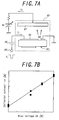
- Figure 7 is a diagram for explaining the operation of the electron-emitting element according to the present invention.
- a current control element 61 has a structure shown in Figure 1, and the circumstance of the current control element 61 is kept in a vacuum state by a vacuum chamber 62.
- a capacitor 66 is arranged in series between a driving electrode 63 and a common electrode 64 in order to prevent short-circuit between the driving electrode 63 and the common electrode 64.
- a bias voltage Vb is applied to an electron capturing electrode 67 opposite to the driving electrode 63 and the common electrode 64.
- the voltage V1 to be applied to a signal voltage source 65 be -400 V
- the capacity of the capacitor 66 be 500 pF
- the bias voltage be 0 V
- the width of a slit formed by the driving electrode 63 and the common electrode 64 be 10 ⁇ m
- the degree of vacuum inside the vacuum chamber 62 be 1 X 10 -3 Pa
- the current I 1 flowing through the driving electrode 63 becomes 2.0 A
- the density of a collector current Ic taken from the electron capturing electrode 67 becomes 1.2 A/cm 2 .
- FIG 8 is a diagram for explaining the operation of the other electron-emitting element according to the present invention.
- a current control element 71 has a structure shown in Figure 2, and the circumstance of the current control element 71 is kept in a vacuum state by a vacuum chamber 72.
- an electric field applying portion 76 between a driving electrode 73 and a driving terminal electrode 75 acts as a capacitor in order to prevent short-circuit between the driving electrode 73 and the common electrode 74.
- An electron capturing electrode 77 is opposite to the driving electrode 73 and the common electrode 74.
- the capacity of the electric field applying portion 76 acting as a capacitor be 530 pF
- the width of a slit formed by the driving electrode 73 and the common electrode 74 be 10 ⁇ m
- the degree of vacuum inside the vacuum chamber 72 be 1 X 10 -3 Pa
- the current I 1 flowing through the driving terminal electrode 75 becomes 2.0 A
- the density of a collector current Ic taken from the electron capturing electrode 77 becomes 1.2 A/cm 2 .
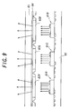
- FIG. 9 is a diagram showing an embodiment of the FED according to the present invention.
- This FED comprises a plurality of electron-emitting elements 81R, 81G and 81B arranged in two dimensions, and a red phosphor 82R, green phosphor 82G and blue phosphor 82B being arranged at a certain space to these electron-emitting elements 81R, 81G and 81B, respectively.
- the electron-emitting elements 81R, 81G and 81B are formed on a substrate 83, and the red phosphor 82R, green phosphor 82G and blue phosphor 82B are formed through the electron capturing electrode 84 on a glass substrate 85.
- the electron-emitting elements 81R, 81G and 81B each have a structure shown in Figure 2, but may have any of the structures shown in Figures 1 and 3 to 6.
- the electron-emitting elements 81R, 81G and 81B are excellent in straight advancing ability, the crosstalk is smaller compared with a case of having conventional electron-emitting elements and the pitch between the phosphors 82R, 82G and 82B can be narrower, and it is not necessary to provide a grid in order to prevent electrons from striking on adjacent phosphors 82R, 82G and 82B.
- the FED of this embodiment is preferable from the viewpoint of downsizing and cost reduction. Since it can emit electrons even if the degree of vacuum is comparatively low, it is not necessary to leave a margin for a lowering of vacuum by making the vacuum space large in advance and thus restrictions against making the FED thin-sized are reduced.
- Figure 10 is a diagram showing the relation between the relative dielectric constant of an electron-emitting element according to the present invention and an applied voltage to it
- Figure 11 is a diagram for explaining it.
- the characteristic of Figure 10 shows the relation between the relative dielectric constant of an electric field applying portion and the applied voltage required for emission of electrons in case that each of the widths d1 and d2 of slits formed by a driving electrode 91 and common electrodes 92a to 92c as shown in Figure 11 is 10 ⁇ m.
- the relative dielectric constant is preferably not less than 1000.
- Figure 12 is a diagram showing the relation between the width of a slit of the electron-emitting element according to the present invention and an applied voltage to it. From Figure 12 it is known that it is necessary to make the slit width be not more than 500 ⁇ m in order to make an electron emission phenomenon occur. In order to drive the electron-emitting element according to the present invention by means of a driver IC to be used in a plasma display, a fluorescent display tube or a liquid crystal display which are on the market, it is necessary to make the slit width be not more than 20 ⁇ m.
- Figure 13A is a top view of a seventh embodiment of the electron-emitting element according to the present invention
- Figure 13B is a sectional view taken along a line VII-VII of it.
- a driving electrode 102 and a common electrode 103 each being in the shape of a semicircle are formed on one side of an electric field applying portion 101, and a conductive coating portion 104 is applied to the driving electrode 102, the common electrode 103 and a slit formed by them.
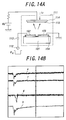
- the operation of the electron-emitting element having a structure shown in Figure 13 is described with reference to Figure 14.
- the periphery of the electron-emitting element is kept in a vacuum state by a vacuum chamber 111.
- a capacitor 113 is arranged in series between the driving electrode 102 and the voltage signal source 112 in order to prevent short-circuit between the driving electrode 102 and the common electrode 103.
- An electron capturing electrode 114 opposite to the driving electrode 102 and the common electrode 103 has a phosphor 115 provided on it and has a bias voltage Vb applied to it.
- the driving electrode 102 and the common electrode 103 each are an Au film of 3 ⁇ m in thickness, and a conductive coating portion 104 made of carbon (of 3 ⁇ m in film thickness) is applied to these driving electrode 102 and common electrode 103 and the slit part therebetween.
- a current Ic flowing through the electron capturing electrode 114 becomes 0.1 A and a current of about 40% of a current I 1 (0.25 A) flowing through the driving electrode 102 is taken as an electron current, and a voltage Vs between the driving electrode 102 and the common electrode 103, namely, a voltage required for emission of electrons becomes 23.8 V.
- the conductive coating 104 functions as a protective layer for the driving electrode 102 and/or the common electrode 103. Concretely, the conductive coating 104 prevents the ions and/or the electrons from colliding the driving electrode 102 and/or the common electrode 103; such ions and/or electrons occurring near the slit when emitting the electron, after then, these ions and/or electrons being accelerated by applying the voltage to the electron-emitting element; and also prevents the generation of heat caused by such a collision from damaging the driving electrode 102 and/or the common electrode 103. In this respect, it is preferable for the conductive coating 104 to be composed of a material with a small sputtering yield and a high melting point.
- the conductive coating 104 is composed of carbon or a conductor with resistance to a high-temperature oxidizing atmosphere, for example, a single metal, an alloy, a mixture of an insulating ceramic and a single metal, a mixture of an insulating ceramic and an alloy or the like, and is preferably composed of a high-melting point precious metal such as platinum, palladium, rhodium, molybdenum or the like, or a material having such an alloy as silver-palladium, silver-platinum, platinum-palladium or the like as its main ingredient, or a cermet material of platinum and ceramic. More preferably, it is composed of only platinum or a material having a platinum-based alloy as its main ingredient.
- the conductive coating portion 104 has the resistance between several k ⁇ and 100 k ⁇ , for example.
- the conductive coating portion 104 is formed by carbon membrane made by vacuum evaporation (for example, the membrane made from "CARBON 5PC" (made by SANYU KOGYO) by vacuum evaporation), rubbed-in carbon (for example, "FW200" (made by Degussa)), or printed carbon.
- the conductive layer coated by the film of alkaline metal oxide or alkaline-earth metals oxide, especially the magnesium oxide is also preferably used as the conductive coating.
- Figure 15A is a top view of an eighth embodiment according to the present invention, and Figure 15B is a sectional view of it taken along line VIII-VIII.
- This embodiment forms a semicircle-shaped driving electrode 112 and a common electrode 113 on one side of an electric field applying portion 111, forms a conductive coating portion 114a on the driving electrode 112, and forms a conductive coating portion 114b being in no contact with the conductive coating portion 114a on the common electrode 113.
- Such an electron-emitting element is obtained by forming a driving electrode 122 and a common electrode 123 on one side of an electric field applying portion 121 by means of printing and then forming a coating portion 125 by means of carbon-vapor deposition of a conductive material on the driving electrode 122, the common electrode 123 and a slit 124 formed by these electrodes to ( Figure 16A), irradiating the slit 124 with a laser beam 127 from a laser irradiating source 126 ( Figure 16B), and thereby forming a conductive coating portion 125a and a conductive coating portion 125b being in no contact with the conductive coating portion 125a.
- An electron-emitting element of a structure shown in Figure 16C can be also obtained by forming a driving electrode 122 and a common electrode 123 on one side of an electric field applying portion 121 by means of printing and then forming a conductive coating portion 125a and a conductive coating portion 125b being in no contact with the conductive coating portion 125a by means of printing. And an electron-emitting element of a structure shown in Figure 16C can be also obtained by applying a thin-film technology such as photolithography.
- the possibility of damaging the driving electrode and common electrode due to collision or heat generation of electrons or ions is remarkably reduced thanks to the first conductive coating portion and the second conductive coating portion being in no contact with the first coating portion, and a driving voltage in case of using the electron-emitting element in a driving circuit is greatly reduced.
- a great reduction in the driving voltage is described in detail.
- an equivalent circuit a between the driving electrode 132 and the common electrode 134 has a resistor a1 and a capacitor a2 connected in parallel with this resistor a1 ( Figure 17B).
- a capacitor 135 for cutting off a direct current is provided between the signal voltage source 133 and the electron-emitting element.
- an equivalent circuit b between the driving electrode 142 and the common electrode 144 has a capacitor b1 only ( Figure 17D). Since the equivalent circuit b has no resistor, it becomes unnecessary to provide a capacitor for cutting off a direct current between the signal voltage source 143 and the electron-emitting element.
- the driving voltage is not divided by a capacitor for cutting off a direct current, a driving voltage used in a driving circuit is more greatly reduced in comparison with said seventh embodiment and driving at a high voltage becomes unnecessary, and as a result, the circuit can be made lower in cost.
- Figure 18A is a top view of a ninth embodiment of an electron-emitting element according to the present invention
- Figure 18B is a sectional view of it taken along line IX-IX.
- This embodiment forms a semicircle-shaped driving electrode 202 and a common electrode 203 on one side of an electric field applying portion 201, forms a conductive coating portion 204a on the driving electrode 202, and forms a conductive coating portion 204b being in no contact with the conductive coating portion 204a on the common electrode 203.
- this electron-emitting element forms a high resistance portion 205 which is composed of a material being higher in resistivity than the conductive coating portions 204a and 204b and is in electric contact with the conductive coating portions 204a and 204b in a slit formed by the driving electrode 202 and the common electrode 203.
- An equivalent circuit between the driving circuit 202 and the common electrode 203 has, as shown in Figure 18C, a terminal x1, resistors x2, x3 and x4 and a terminal x5 respectively corresponding to the driving electrode 202, the conductive coating portion 204a, the high resistance portion 205, the conductive coating portion 204b and the common electrode 203.
- a voltage is applied to the electron-emitting element, the voltage of the high resistance portion 205 becomes higher than the voltage of the conductive coating portions 204a and 204b, and the degree of concentration of electric field in the high resistance portion, namely, in the slit is improved.
- it is possible to emit electrons at a low applied voltage reduce the power consumption, miniaturize the circuit of the electron-emitting element and attain a cost reduction thanks to omitting high-voltage components.
- Figure 19 is a diagram showing a variation example of the electron-emitting element of Figure 18.
- a high resistance portion which is composed of a material being higher in resistivity than two conductive coating portions being in no contact with each other and is in electric contact with these conductive coating portions is provided in a slit formed by a driving electrode and a common electrode.
- a high resistance portion which is composed of the same material as two conductive coating portions being in no contact with each other and is thinner in thickness than these conductive coating portions is provided in a slit formed by a driving electrode and a common electrode.
- Such a high resistance portion can be obtained, for example, by irradiating the conductive coating portion on the slit with a laser and forming a conductive coating portion being thinner in thickness in comparison with the conductive coating portions formed on the driving and common electrodes.
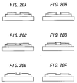
- FIG 20 is a diagram showing a tenth embodiment of an electron-emitting element according to the present invention.
- This embodiment is an electron-emitting element provided on a zirconium oxide (zirconia) substrate, and on the zirconium oxide substrate there is arranged, for example, an electron-emitting element shown in Figure 13 ( Figure 20A), an electron-emitting element shown in Figure 15 (Figure 20B), an electron-emitting element shown in Figure 18 (Figure 20C), an electron-emitting element shown in Figure 19A ( Figure 20D), an electron-emitting element shown in Figure 19B ( Figure 20E) or an electron-emitting element shown in Figure 19C ( Figure 20F).
- forming a substrate out of zirconium oxide is preferable from the viewpoint of strength, tenacity and durability.
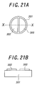
- Figure 21A is a top view of a eleventh embodiment of the electron-emitting element according to the present invention
- Figure 21B is a sectional view taken along a line X-X of it.
- a driving electrode 302 and a common electrode 303 each being in the shape of a semicircle are formed on one side of an electric field applying portion 301.
- a material for each of the driving electrode 302 and the common electrode 303 is Au, and in case of making a voltage Vk to be applied to the signal voltage source 312 be 160 V, making the capacity of the capacitor 313 be 5 nF, making the bias voltage Vb be 300 V, forming the electric field applying portion 301 out of an electrostrictive material of 4,500 in relative dielectric constant, making the width of a slit formed by the driving electrode 302 and the common electrode 303 be 10 ⁇ m, and making the degree of vacuum inside the vacuum chamber 311 be 200 Pa or less, a current Ic flowing through the electron capturing electrode 314 becomes 1.2 A and a current of about 60% of a current I 1 (2 A) flowing through the driving electrode 302 is taken as an electron current, and a voltage Vs between the driving electrode 302 and the common electrode 303, namely, a voltage required for emission of electrons becomes 153 V.
- the waveforms of the currents I 1 , I 2 and Ic, and the voltage Vs are respectively shown by curves i
- the electron-emitting element according to the present invention can emit electrons at a very low vacuum of not more than 200 Pa, in case of forming an FED, it is possible to make very small a sealed space of the outer circumferential part of a panel, and thus it is possible to realize a narrow-frame panel. And in case of make a large-sized display by arranging a plurality of panels, a joint between panels is made hard to be conspicuous.
- a conventional FED the degree of vacuum of a space inside the FED is lowered by gas produced from a phosphor and the like and there is the possibility that the durability of a panel receives a bad influence, but since a display using the electron-emitting element according to the present invention can emit electrons at a very low vacuum of not more than 200 Pa, a bad influence caused by lowering of the degree of vacuum of a space inside the FED is greatly reduced and the durability and reliability of the panel are greatly improved.
- the electron-emitting element according to the present invention and the FED using it can be more simplified and made more small-sized in comparison with those of the prior art. Concretely explaining them, first since the degree of vacuum in a space inside an FED can be made low, an enclosure supporting structure facing a pressure difference between the inside and the outside of the outer circumferential sealed part and the like of an FED can be simplified and made small-sized.
- a bias voltage to be applied to the electron capturing electrode may be 0 V.
- the electric field applying portion of the electron-emitting element according to the present invention can be formed without the need of a special processing as required in case of forming an electron-emitting element of a Spindt type and furthermore the electrodes and the electric field applying portion can be formed by a thick film printing method, an electron-emitting element according to the present invention and an FED using it can be manufactured in lower cost in comparison with those of the prior art.
- an applied voltage necessary for emitting electrons and a bias voltage to be applied to an electron capturing electrode can be made comparatively low, a driving IC being comparatively low in dielectric strength, small-sized and inexpensive can be used and therefore an FED using an electron-emitting element according to the present invention can be manufactured in low cost.
- the present invention is not limited to the embodiments described above but can be variously modified and varied in many manners.
- the electron-emitting element according to the present invention can be also applied to another application such as backlighting. Since the electron-emitting element according to the present invention can emit a comparatively large amount of electron beam at a comparatively low voltage, it is preferable for forming a small-sized and high-efficiency sterilizer in place of a conventional sterilizer using mainly an ultraviolet ray emission method. And the electron-emitting element according to the present invention can adopt any other electrode structure having an angular part. Further, it can arrange a resistor in series between a second electrode, namely, a common electrode and a direct offset voltage source in order to prevent short-circuit between a driving electrode and a common electrode.
- the electric field applying portions 51a, 51b are formed out of an antiferroelectric material has been described, but it is enough that the electric field applying portions 51a, 51b are formed out of at least one of a piezoelectric material, an electrostrictive material and an antiferroelectric material.
- a material having lead zirconate (PZ-based) as its main ingredient a material having nickel lead niobate as its main ingredient, a material having zinc lead niobate as its main ingredient, a material having manganese lead niobate as its main ingredient, a material having magnesium lead tantalate as its main ingredient, a material having nickel lead tantalate as its main ingredient, a material having antimony lead stannate as its main ingredient, a material having lead titanate as its main ingredient, a material having magnesium lead tungstate as its main ingredient, a material having cobalt lead niobate as its main ingredient, or a composite material containing an optional combination of these materials, and among them a ceramic material containing lead zirconate is most frequently used as a piezoelectric material and/or an electrostrictive material.
- PZ-based lead zirconate
- a proper material obtained by properly adding an oxide of lanthanum, barium, niobium, zinc, cerium, cadmium, chromium, cobalt, antimony, iron, yttrium, tantalum, tungsten, nickel, manganese, lithium, strontium, bismuth or the like, or a combination of some of these materials or other compounds to the ceramic material for example, a material obtained by adding a specific additive to it so as to form a PZT-based material is also preferably used.
- a multiple-component piezoelectric material and/or electrostrictive material its piezoelectric and/or electrostrictive characteristics vary depending upon the composition of their components, and a three-component material of magnesium lead niobate-lead zirconate-lead titanate, or a four-component material of magnesium lead niobate-nickel lead tantalate-lead zirconate-lead titanate or a four-component material of magnesium lead tantalate-magnesium lead niobate-lead zirconate-lead titanate preferably has the composition in the vicinity of the phase boundary of pseudo-cubic system-tetragonal system-rhombohedral system, and particularly the composition of magnesium lead niobate of 15 to 50 mol%, lead zirconate of 10 to 45 mol% and lead titanate of 30 to 45 mol%, the composition of magnesium lead niobate of 15 to 50 mol%, nickel lead tantalate
- the high resistance portion may be of a material having a conductive material sparsely distributed in it, a material changed in structure by locally destroying, deforming or changing in property a conductive material in it, a material changed in structure or microcracked by processing a conductive coating portion by means of application of a high voltage or the like and by locally destroying, deforming or changing in property a conductive material in it, a material whose resistance value is made high by a fact that the slit expands due to a piezoelectric effect only when applying an electric field, or a material whose resistance value is made high by a fact that it is microcracked due to a piezoelectric effect.
Landscapes
- Engineering & Computer Science (AREA)
- Physics & Mathematics (AREA)
- Computer Hardware Design (AREA)
- General Physics & Mathematics (AREA)
- Theoretical Computer Science (AREA)
- Cathode-Ray Tubes And Fluorescent Screens For Display (AREA)
- Cold Cathode And The Manufacture (AREA)
- Electrodes For Cathode-Ray Tubes (AREA)
Abstract
Description
Claims (18)
- An electron-emitting element comprising:an electric field applying portion composed of a dielectric;a first electrode formed on one surface of this electric field applying portion; anda second electrode formed on said one surface of the electric field applying portion, and forming a slit in cooperation with said first electrode.
- An electron-emitting element comprising:an electric field applying portion composed of at least one of a piezoelectric material, an electrostrictive material and an antiferroelectric material;a first electrode formed on one surface of this electric field applying portion; anda second electrode formed on said one surface of the electric field applying portion, and forming a slit in cooperation with said first electrode.
- An electron-emitting element according to claim 1 or 2, further comprising a third electrode arranged at a certain space to said first and second electrodes, wherein space between said first and second electrodes and said third electrode is vacuum.
- An electron-emitting element according to claim 2, wherein said electric field applying portion also acts an actuator and controls the quantity of emitted electrons by the displacement motion of said electric field applying portion.
- An electron-emitting element according to claim 3, further comprising:a voltage source for applying a direct offset voltage to said third electrode; anda resistor arranged in series between this voltage source and said third electrode.
- An electron-emitting element according to any one of claims 1 to 5, wherein a conductive coating portion is applied to said first electrode, said second electrode and said slit.
- An electron-emitting element according to any one of claims 1 to 6, wherein further comprising a first conductive coating portion provided on said first electrode; andwherein, there is non-contact condition between said first conductive coating portion and said second conductive coating portion.a second conductive coating portion provided on said second electrode;
- An electron-emitting element according to claim 7, wherein a portion with a high resistance being provided on said slit, said portion having a higher resistance than those of said first and said second conducting coating portions and being in contact with said first and said second conducting coating portions electrically.
- An electron-emitting element according to any one of claims 1 to 8, wherein a pulse voltage is applied to said first electrode and a direct offset voltage is applied to said second electrode.
- An electron-emitting element according to any one of claims 1 to 9, further comprising a capacitor arranged in series between said first electrode and said voltage source.
- An electron-emitting element according to any one of claims 1 to 10, further comprising a fourth electrode formed on the other surface of said electric field applying portion and facing to said first electrode.
- An electron-emitting element according to any one of claims 1 to 11, further comprising a resistor arranged in series between said second electrode and a direct offset voltage source.
- An electron-emitting element according to any one of claims 1 to 12, wherein said electric field applying portion has the relative dielectric constant not less than 1000.
- An electron-emitting element according to any one of claims 1 to 13, wherein said slit has the width not more than 500µm.
- An electron-emitting element according to any one of claims 1 to 14, wherein at least one of said first electrode and said second electrode has an angular part with an acute angle.
- An electron-emitting element according to any one of claims 1 to 15, wherein said first electrode and said second electrode each have carbon nanotubes.
- A field emission display comprising:a plurality of electron-emitting elements according to any one of claims 1 to 16 arranged in two dimensions; anda plurality of phosphors each being arranged with a certain space to each of these electron-emitting elements.
- A field emission display according to claim 17, further comprising a substrate having a plurality of electron-emitting elements arranged in two dimensions and formed into one body with each other.
Applications Claiming Priority (10)
| Application Number | Priority Date | Filing Date | Title |
|---|---|---|---|
| US10/027,232 US7088049B2 (en) | 2000-12-22 | 2001-12-20 | Electron-emitting device and field emission display using the same |
| US27232 | 2001-12-20 | ||
| JP2002049754 | 2002-02-26 | ||
| JP2002049754 | 2002-02-26 | ||
| JP2002183481 | 2002-06-24 | ||
| JP2002183481 | 2002-06-24 | ||
| US10/206,409 US20030038600A1 (en) | 2000-12-22 | 2002-07-26 | Electron-emitting device and field emission display using the same |
| US206409 | 2002-07-26 | ||
| JP2002319761A JP3848237B2 (en) | 2001-12-20 | 2002-11-01 | Electron emitting device and field emission display using the same |
| JP2002319761 | 2002-11-01 |
Publications (2)
| Publication Number | Publication Date |
|---|---|
| EP1329928A2 true EP1329928A2 (en) | 2003-07-23 |
| EP1329928A3 EP1329928A3 (en) | 2006-02-08 |
Family
ID=27532074
Family Applications (1)
| Application Number | Title | Priority Date | Filing Date |
|---|---|---|---|
| EP02258747A Withdrawn EP1329928A3 (en) | 2001-12-20 | 2002-12-18 | Electron-emitting element and field emission display using the same |
Country Status (2)
| Country | Link |
|---|---|
| EP (1) | EP1329928A3 (en) |
| JP (1) | JP3848237B2 (en) |
Cited By (2)
| Publication number | Priority date | Publication date | Assignee | Title |
|---|---|---|---|---|
| CN105097380A (en) * | 2014-05-22 | 2015-11-25 | 中国科学院苏州纳米技术与纳米仿生研究所 | Field emission device and manufacturing method thereof |
| CN107346720A (en) * | 2016-05-04 | 2017-11-14 | 中国科学院苏州纳米技术与纳米仿生研究所 | Feds and preparation method thereof |
Families Citing this family (2)
| Publication number | Priority date | Publication date | Assignee | Title |
|---|---|---|---|---|
| JP4662140B2 (en) * | 2004-07-15 | 2011-03-30 | 日本碍子株式会社 | Electron emitter |
| JP5053524B2 (en) * | 2005-06-23 | 2012-10-17 | 日本碍子株式会社 | Electron emitter |
Family Cites Families (14)
| Publication number | Priority date | Publication date | Assignee | Title |
|---|---|---|---|---|
| JP2654571B2 (en) * | 1988-06-10 | 1997-09-17 | キヤノン株式会社 | Electron-emitting device, electron-emitting device and light-emitting device using the same |
| JPH07147131A (en) * | 1993-11-24 | 1995-06-06 | Tdk Corp | Cold cathode electron source manufacturing method |
| US5831387A (en) * | 1994-05-20 | 1998-11-03 | Canon Kabushiki Kaisha | Image forming apparatus and a method for manufacturing the same |
| JPH08264105A (en) * | 1995-03-27 | 1996-10-11 | Kanebo Ltd | Ferroelectric electron emission cold cathode |
| JPH0927273A (en) * | 1995-07-12 | 1997-01-28 | Canon Inc | Electron-emitting device, electron source, image forming apparatus using the same, and manufacturing method thereof |
| JPH0945226A (en) * | 1995-07-31 | 1997-02-14 | Canon Inc | Electron emitting device, electron source and image forming apparatus using the same, and manufacturing method thereof |
| JPH0990882A (en) * | 1995-09-20 | 1997-04-04 | Komatsu Ltd | Light-emitting display element |
| JP3376220B2 (en) * | 1995-10-03 | 2003-02-10 | キヤノン株式会社 | Image forming apparatus and manufacturing method thereof |
| JP3320333B2 (en) * | 1996-04-30 | 2002-09-03 | キヤノン株式会社 | Electron emitting device, image forming apparatus using the same, and method of manufacturing the same |
| JPH11317149A (en) * | 1998-05-01 | 1999-11-16 | Canon Inc | Electron emitting device and method of manufacturing the same |
| FR2789221B1 (en) * | 1999-01-29 | 2001-04-06 | Univ Nantes | CATHODE BODY FOR THE EMISSION OF ELECTRON |
| JP2000285801A (en) * | 1999-03-31 | 2000-10-13 | Canon Inc | Method of manufacturing electron-emitting device, electron source using the electron-emitting device, and image forming apparatus |
| EP1073090A3 (en) * | 1999-07-27 | 2003-04-16 | Iljin Nanotech Co., Ltd. | Field emission display device using carbon nanotubes and manufacturing method thereof |
| JP3699451B2 (en) * | 2000-12-22 | 2005-09-28 | 日本碍子株式会社 | Electron emitting device and field emission display using the same |
-
2002
- 2002-11-01 JP JP2002319761A patent/JP3848237B2/en not_active Expired - Fee Related
- 2002-12-18 EP EP02258747A patent/EP1329928A3/en not_active Withdrawn
Cited By (5)
| Publication number | Priority date | Publication date | Assignee | Title |
|---|---|---|---|---|
| CN105097380A (en) * | 2014-05-22 | 2015-11-25 | 中国科学院苏州纳米技术与纳米仿生研究所 | Field emission device and manufacturing method thereof |
| WO2015176596A1 (en) * | 2014-05-22 | 2015-11-26 | 中国科学院苏州纳米技术与纳米仿生研究所 | Field emission device and preparation method therefor |
| CN105097380B (en) * | 2014-05-22 | 2017-10-24 | 中国科学院苏州纳米技术与纳米仿生研究所 | A kind of feds and preparation method thereof |
| CN107346720A (en) * | 2016-05-04 | 2017-11-14 | 中国科学院苏州纳米技术与纳米仿生研究所 | Feds and preparation method thereof |
| CN107346720B (en) * | 2016-05-04 | 2020-09-01 | 中国科学院苏州纳米技术与纳米仿生研究所 | Field emission device and manufacturing method thereof |
Also Published As
| Publication number | Publication date |
|---|---|
| JP2004087450A (en) | 2004-03-18 |
| EP1329928A3 (en) | 2006-02-08 |
| JP3848237B2 (en) | 2006-11-22 |
Similar Documents
| Publication | Publication Date | Title |
|---|---|---|
| US7088049B2 (en) | Electron-emitting device and field emission display using the same | |
| US7842398B2 (en) | Dielectric device | |
| US20040090398A1 (en) | Display | |
| EP1403895A2 (en) | Light emission device and field emission display having such light emission devices. | |
| JP3822551B2 (en) | Light emitting device and field emission display including the same | |
| JP3867065B2 (en) | Electron emitting device and light emitting device | |
| US6936972B2 (en) | Electron-emitting element and field emission display using the same | |
| US20060192213A1 (en) | Light-emitting device | |
| US20040085010A1 (en) | Electron emitter, drive circuit of electron emitter and method of driving electron emitter | |
| JP3848237B2 (en) | Electron emitting device and field emission display using the same | |
| US20030038600A1 (en) | Electron-emitting device and field emission display using the same | |
| US6897620B1 (en) | Electron emitter, drive circuit of electron emitter and method of driving electron emitter | |
| JP3869819B2 (en) | Electron emitter | |
| JP3867078B2 (en) | Electron emitter | |
| JP3829127B2 (en) | Electron emitter | |
| US20080048569A1 (en) | Dielectric element and electron emitter | |
| JP3839792B2 (en) | Electron emission method of electron-emitting device | |
| JP2006278319A (en) | Light source | |
| JP3829128B2 (en) | Electron emitter | |
| US7576479B2 (en) | Electron emitter | |
| US20050073232A1 (en) | Electron emitter | |
| US7719201B2 (en) | Microdevice, microdevice array, amplifying circuit, memory device, analog switch, and current control unit | |
| EP1635370A1 (en) | Electron-emitting apparatus | |
| EP1521230A2 (en) | Electron emitter display device having micro-display array, amplifying circuit, memory device, analog switch, and current control unit | |
| JP4097230B2 (en) | Electron emitter |
Legal Events
| Date | Code | Title | Description |
|---|---|---|---|
| PUAI | Public reference made under article 153(3) epc to a published international application that has entered the european phase |
Free format text: ORIGINAL CODE: 0009012 |
|
| AK | Designated contracting states |
Designated state(s): AT BE BG CH CY CZ DE DK EE ES FI FR GB GR IE IT LI LU MC NL PT SE SI SK TR |
|
| AX | Request for extension of the european patent |
Extension state: AL LT LV MK RO |
|
| PUAL | Search report despatched |
Free format text: ORIGINAL CODE: 0009013 |
|
| AK | Designated contracting states |
Kind code of ref document: A3 Designated state(s): AT BE BG CH CY CZ DE DK EE ES FI FR GB GR IE IT LI LU MC NL PT SE SI SK TR |
|
| AX | Request for extension of the european patent |
Extension state: AL LT LV MK RO |
|
| RIC1 | Information provided on ipc code assigned before grant |
Ipc: G09G 3/22 20060101ALI20051221BHEP Ipc: H01J 1/316 20060101ALI20051221BHEP Ipc: H01J 1/304 20060101AFI20030512BHEP |
|
| 17P | Request for examination filed |
Effective date: 20060210 |
|
| AKX | Designation fees paid |
Designated state(s): DE FR GB IT NL |
|
| 17Q | First examination report despatched |
Effective date: 20080411 |
|
| STAA | Information on the status of an ep patent application or granted ep patent |
Free format text: STATUS: THE APPLICATION IS DEEMED TO BE WITHDRAWN |
|
| 18D | Application deemed to be withdrawn |
Effective date: 20081022 |