EP1329805A2 - Laden und Interpretieren von Daten - Google Patents
Laden und Interpretieren von Daten Download PDFInfo
- Publication number
- EP1329805A2 EP1329805A2 EP03000523A EP03000523A EP1329805A2 EP 1329805 A2 EP1329805 A2 EP 1329805A2 EP 03000523 A EP03000523 A EP 03000523A EP 03000523 A EP03000523 A EP 03000523A EP 1329805 A2 EP1329805 A2 EP 1329805A2
- Authority
- EP
- European Patent Office
- Prior art keywords
- data
- word
- memory
- processor core
- order
- Prior art date
- Legal status (The legal status is an assumption and is not a legal conclusion. Google has not performed a legal analysis and makes no representation as to the accuracy of the status listed.)
- Withdrawn
Links
Images

Classifications
-
- G—PHYSICS
- G06—COMPUTING OR CALCULATING; COUNTING
- G06F—ELECTRIC DIGITAL DATA PROCESSING
- G06F12/00—Accessing, addressing or allocating within memory systems or architectures
- G06F12/02—Addressing or allocation; Relocation
- G06F12/04—Addressing variable-length words or parts of words
-
- G—PHYSICS
- G06—COMPUTING OR CALCULATING; COUNTING
- G06F—ELECTRIC DIGITAL DATA PROCESSING
- G06F9/00—Arrangements for program control, e.g. control units
- G06F9/06—Arrangements for program control, e.g. control units using stored programs, i.e. using an internal store of processing equipment to receive or retain programs
- G06F9/30—Arrangements for executing machine instructions, e.g. instruction decode
- G06F9/30003—Arrangements for executing specific machine instructions
- G06F9/30007—Arrangements for executing specific machine instructions to perform operations on data operands
- G06F9/30032—Movement instructions, e.g. MOVE, SHIFT, ROTATE, SHUFFLE
Definitions
- the invention relates generally to loading data into a memory portable data carrier as well as interpreting data in the Memory of the portable storage device are present, by one of one Processor core of the portable data carrier running interpreter.
- special The invention relates to the loading and interpretation of data, the multi-word data structures included with a given word order.
- portable data carriers used in connection with the invention can in particular be a chip card in different designs or Be chip module.
- a "bit field” is to be understood here as a bit field, the width of which corresponds to the processing width of the processor core and of the memory. For a portable data carrier with an 8-bit processing width, a word is therefore equal to one byte.
- the native read or write access to multi-word data structures by the processor core of the portable data carrier presupposes that the data in the memory have a word order predetermined by the hardware or micro-programming of the processor core. If this is not the case, for example if the processor core expects a little-endian word order and the multi-word data structures are stored in big-endian word order, the native processor functions cannot be used.
- the read or write access must then take place in several individual steps in which the individual memory words of the multi-word data structure are accessed separately and in which shifting and linking operations are carried out. Compared to the native access operation, these single steps are very inefficient.
- CAP converted applet
- the CAP format is described in detail in Chapter 6 of the document " Java Card TM 2.2.1 Virtual Machine Specification ", Revision 1.0 dated May 18, 2000, available at http: // java.sun.com / products / javacard .
- CAP data is a sequence of 8-bit words that have instruction codes and data values with an 8-bit width and multi-word data structures with 16 or 32 bits. All multi-word data structures are available in the CAP data in big-endian word order.
- Some known circuits are based on processors that "master" both word orders.
- DE 43 12 250 A1 describes a computer system which allows both the processing of big-endian and little-endian word orders.
- the system includes a suitable processor that can process both word orders.
- the processor is set to a suitable word order by software-controlled changes in the firmware.
- US 5,848,43 discloses an effective memory management system for a processor which can be operated on the one hand using the big-endian word order and on the other hand using a so-called modified little-endian word order.
- the addresses of the data to be stored are changed using certain bit patterns.
- the invention has for its object to provide a technique through which Data with a given word order efficiently into portable data carriers, that require a different word order, load or onto the data carrier have it interpreted.
- the object of the invention is to solve the problems mentioned at least in part to avoid and to provide a technology through which data can be used a given word order efficiently into portable media, which is a assume different word order, load or interpret on the data carriers to let.
- no additional hardware is required for this and the data are not intended to limit the Alignment of the multi-word data structures are subject.
- the invention is based on the basic idea the data falling without changing their relative order or increasing addresses in the memory, so that the word order the stored data with the native word order of the processor core matches.
- the data is therefore stored as a whole memory area when it is loaded "reversed” filed. In many configurations, this means that the data starts at high memory addresses towards low addresses be written into memory.
- the invention enables data to be loaded into memory without or with little additional effort.
- the data does not need to be analyzed for the presence of multi-word data structures, what the computing time and also the memory requirement during the loading process reduced.
- the number of memory accesses is minimal.
- memory operations can be used in blocks that are significantly more efficient than individual access.
- the base address for access to a multi-word data structure serving as the parameter of an instruction code to choose a native processor function to access the multi-word data structures can be used.
- the invention is essentially based on the knowledge that the counterintuitive step of loading the data in the "wrong” order is not only harmless, but also brings considerable advantages. In particular it is a surprising result that the "wrong" stored Have data interpreted extremely efficiently.
- the native word order of the processor core is a little-endian word order
- the word order of the multi-word data structures in the data to be loaded is a big-endian word order.
- the data written according to the invention in the “reverse” direction then have a little-endian word order.
- the writing process is preferably carried out in the direction from high to low addresses.
- the intended direction of the program flow from instruction code to instruction code, if jump instructions are not taken into account, preferably also runs from high to low addresses. In other configurations of the invention, however, the arrangements mentioned here are precisely the reverse.
- the invention is particularly preferably used for portable data carriers which have the functionality of a Java Card TM.
- the interpreter executed by the processor core is then preferably a Java Card Virtual Machine .
- the data to be loaded into the data carrier are preferably in the Java Card CAP format.
- the computer-readable data carrier has program instructions to implement the inventive method.
- a data carrier can be, for example, a semiconductor memory or a floppy disk or a CD-ROM or a tape on which an interpreter and / or a loading program for use in chip cards according to the invention is stored is.
- such a data carrier can be used be provided in the production of chip cards.
- the computer-readable data carrier and / or the portable data carrier with features that the described above and / or in the dependent method claims correspond to the mentioned characteristics.
- the portable data carrier 10 shown in FIG. 1 is designed as a chip card in the present exemplary embodiment. It has an interface 12 for contactless or contact-based data exchange with the environment, a processor core 14 and a memory 16.
- the processor core 14, the memory 16 and parts of the interface 12 are integrated on a single semiconductor chip, not shown separately in FIG. 1.
- the memory 16 has several areas that are in different memory technologies are designed. In the embodiment of FIG. 1 these are, for example, a ROM programmed as a mask Read-only memory 18, a non-volatile designed in EEPROM technology Read / write memory 20 and a volatile RAM Read / write memory 22.
- the read-only memory 18 contains, in particular an operating system 24, a loader 26 and an interpreter 28.
- the operating system 24 provides basic functions for the operation of the portable data carrier 10 in a manner known per se.
- the interpreter 28 implements a Java Card Virtual Machine, which is available under http: // java.sun.com according to the already mentioned document "Java Card TM 2.2.1 Virtual Machine Specification ", Revision 1.0 of May 18, 2000 / products / javacard .
- the load program 26 serves to load data 30 into the memory 16.
- the data written into the non-volatile read / write memory 20 as a result of the loading process are provided with the reference symbol 32 in the figures.
- the data 30 are in the Java Card CAP format already mentioned at the beginning.
- the data 30 can have other structured and / or interpretable data formats.
- the data 30 is a sequence of bytes by which instructions of a Java card applet are encoded. Each instruction has a byte as instruction code and optionally one or more parameters.
- the parameters can be single bytes or two-word data structures with two bytes (data type short ) or four-word data structures with four bytes (data type integer ). All multi-word data structures in the data 30 to be loaded have the big-endian word order.
- the first byte of the data 30 to be loaded is shown in Figures 2-4 below. This byte denotes the sipush command as the first instruction code 0x13 .
- the command sipush causes the 2-byte constant 0xABCD, which is specified by the multi-word data structure 34 following as a parameter, to be written into a stack.
- the instruction code 0x16 designates the command SLOAD, and the 1-byte parameter 0x12 is a local variable index on it.
- the instruction code 0x8D in the third instruction calls a method (command invokestatic ).
- the multi-word data structure 36 specifies the index value 0x0123 as a parameter. This index value refers to an entry in a constant pool, which in turn references the method to be called.
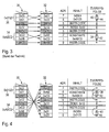
- the data 30 are retained their order in ascending order in the memory 16 loaded; the charging process is symbolized by arrows.
- the loading process is the first instruction code 0x13 at memory address 0 relative to a start address of the one under consideration here Memory area, the most significant byte 0xAB of the multi-word data structure 34 at memory address 1, the lesser byte 0xCD of the multi-word data structure 34 at memory address 2, and so on.
- the loading and interpretation method illustrated in FIG. 3 avoids the considerable additional outlay which is required in the method of FIG. 2 for the data format conversion during the interpretation time.
- the structure of the data 30 is analyzed at the loading time in order to identify the multi-word data structures 34 and 36.
- the bytes of these multi-word data structures 34 and 36 are then exchanged during the loading process, so that the data 32 written in the memory 16 at the addresses 1 and 2 or 6 and 7 have the little-endian word order.
- the multi-word data structures 34 and 36 of the data 32 present in the memory 16 can then be read by native commands of the processor core 14 at the time of interpretation. These commands are indicated by ovals in the right column of FIG. 3 and are given the reference symbols 38 and 40, respectively.
- Each native multi-word instruction 38, 40 starts from a base address 42, 44 which specifies the first memory word read.
- the processor core 14 specifies that the address of the least significant word of the multi-word data structure 34, 36 serves as the base address 42, 44.
- the loading of the data 30 is controlled by the loading program 26.
- the data 30 are written to the memory 16 without changing their relative order in the direction of descending addresses. Efficient operations for writing memory 16 in blocks can be used.
- the data 32 loaded into the memory 16 have been swapped overall compared to the original data 30. For example, the instruction codes in the data 32 are arranged at the addresses 7, 4 and 2 and thus have higher addresses than the respectively assigned parameters.
- the multi-word data structures 34, 36 are present in the memory 16 as a result of the loading process in the little-endian word order.
- interpreter 28 interprets that in memory 16 data 32 is the address reversal during the loading process considered.
- the individual instructions are therefore in the direction falling memory addresses executed. This affects both the transition from an instruction code to one or more associated parameters as well as the program flow from one instruction code to the next - without taking jumps into account.
- the The sequence shown in FIG. 4 is first instruction code 0x13 at the memory address 7 evaluated, then the multi-word data structure 34 with the Value 0xABCD at addresses 5 and 6, then the instruction code 0x16 address 4, then its associated parameter 0x12 at address 3, and so on.
- the multi-word data structures 34, 36 as in the method of Fig. 3 by native processor instructions 38, 40 read so that the order of access within a multi-word data structure 34, 36, as specified by the processor core 14, in Direction of increasing addresses.
- the access sequence runs within a multi-word data structure 34, 36 reverse to that direction of instruction execution mentioned above.
- the multi-word data structures 34, 36 used base addresses 42, 44 not directly to the addresses of the corresponding instruction codes, but they are of the instruction codes through the high-order bytes of the multi-word data structures 34, 36 separately.
- FIG. 1 An example of the change of direction just mentioned is shown in FIG the evaluation of the instruction code 0x13 at address 7 address 5 as Base address 42 used by the native processor command 38 to the To access multi-word data structure 34.
- the processor core reads 14 first the lower byte 0xCD of address 5 and then the most significant byte 0xAB of address 6. Before and after execution of processor instruction 38, however, the interpretation process takes place in the direction falling memory addresses.
- the method described here enables efficient interpretation of the data 32 located in the memory 16, it being possible in particular to use native multi-word processor instructions 38, 40. While in the present example the loading and interpretation of data 30, which originally existed in the big-endian word order, was described on a platform with little-endian word order, the techniques according to the invention can also be used accordingly in the reverse case.
Landscapes
- Engineering & Computer Science (AREA)
- Theoretical Computer Science (AREA)
- Physics & Mathematics (AREA)
- General Engineering & Computer Science (AREA)
- General Physics & Mathematics (AREA)
- Software Systems (AREA)
- Devices For Executing Special Programs (AREA)
- Memory System Of A Hierarchy Structure (AREA)
Abstract
Description
Claims (11)
- Verfahren zum Laden von Daten (30) in einen Speicher (16) eines tragbaren Datenträgers (10), bei dem:dadurch gekennzeichnet, daßder tragbare Datenträger (10) einen Prozessorkern (14) aufweist, der dazu eingerichtet ist, in einer vorgegebenen, nativen Wortordnung auf Datenwörter von Mehrwort-Datenstrukturen (34, 36) im Speicher (16) zuzugreifen (38, 40), und bei demdie zu ladenden Daten (16) Mehrwort-Datenstrukturen (34, 36) enthalten, deren Wortordnung gegenüber der nativen Wortordnung des Prozessorkerns (14) umgekehrt ist,die Daten (30) unter Beibehaltung ihrer Reihenfolge aufsteigend bzw. absteigend in den Speicher (16) geschrieben werden, so daß die Wortordnung der im Speicher (16) abgelegten Mehrwort-Datenstrukturen (34,36) mit der nativen Wortordnung des Prozessorkerns (14) übereinstimmt.
- Verfahren nach Anspruch 1, dadurch gekennzeichnet, daß die native Wortordnung des Prozessorkerns (14) eine little-endian-Wortordnung ist, und daß die Wortordnung der Mehrwort-Datenstrukturen (34, 36) in den zu ladenden Daten (30) eine big-endian-Wortordnung ist, in daß die Daten (30) in Richtung absteigender Adressen in den Speicher (16) geschrieben werden, so daß die Wortordnung der in den Speicher (16) geschriebenen Mehrwort-Datenstrukturen (34, 36) eine little-endian-Wortordnung ist.
- Verfahren nach Anspruch 1 oder 2, dadurch gekennzeichnet, daß die Daten (30) Instruktionscodes aufweisen, die zur Interpretierung durch einen von dem Prozessorkern (14) ausgeführten Interpreter (28) des tragbaren Datenträgers (10) vorgesehen sind, und daß zumindest einigen der Instruktionscodes je mindestens eine Mehrwort-Datenstruktur (34, 36) als Parameter zugeordnet ist.
- Verfahren zum Interpretieren von Daten (32), die in einem Speicher (16) eines tragbaren Datenträgers (10) vorliegen, durch einen Interpreter (28), der von einem Prozessorkern (14) des tragbaren Datenträgers (10) ausgeführt wird, wobei:dadurch gekennzeichnet, daßdie Daten (32) Instruktionscodes enthalten, die zur Interpretierung durch den Interpreter (28) vorgesehen sind,zumindest einigen der Instruktionscodes je mindestens eine Mehrwort-Datenstruktur (34, 36) als Parameter zugeordnet ist,der Prozessorkern (14) dazu eingerichtet ist, auf Grundlage einer Basisadresse (42, 44), die eine Mehrwort-Datenstruktur (34, 36) bezeichnet, in einer vorgegebenen, nativen Wortordnung auf die Datenwörter dieser Mehrwort-Datenstruktur zuzugreifen (38, 40),die Adresse jedes Instruktionscodes sich von jeder Basisadresse (42, 44), die zum Zugriff auf eine als Parameter des Instruktionscodes dienende Mehrwort-Datenstruktur (34, 36) verwendet wird, um mehr als die Wortanzahl des Instruktionscodes unterscheidet.
- Verfahren nach Anspruch 4, dadurch gekennzeichnet, daß jeder Instruktionscode sich im Speicher (32) an einer höheren Adresse befindet als alle diesem Instruktionscode zugeordneten Parameter.
- Verfahren nach Anspruch 4 oder Anspruch 5, dadurch gekennzeichnet, d a ß die native Wortordnung des Prozessorkerns (14) eine little-endian-Wortordnung ist, und daß die Wortordnung der im Speicher (16) vorliegenden Mehrwort-Datenstrukturen (34, 36) eine little-endian-Wortordnung ist, und daß die vorgesehene Richtung des Programmflusses von Instruktionscode zu Instruktionscode, ohne Berücksichtigung von Sprungbefehlen, von hohen zu niedrigen Speicheradressen erfolgt.
- Verfahren nach einem der Ansprüche 3 bis 6, dadurch gekennzeichnet, d a ß bei den im Speicher (16) enthaltenen Daten (32) die vorgesehene Richtung des Programmflusses von Instruktionscode zu Instruktionscode, ohne Berücksichtigung von Sprungbefehlen, umgekehrt zu einer durch den Prozessorkern (14) vorgegebenen, nativen Zugriffsreihenfolge auf die einzelnen Datenwörter der als Parameter dienenden Mehrwort-Datenstrukturen (34, 36) ist.
- Verfahren nach einem der Ansprüche 1 bis 7, dadurch gekennzeichnet, d a ß die Wortbreite des Prozessorkerns (14) und des Speichers (16) 8 Bit beträgt, und daß die Mehrwort-Datenstrukturen (34, 36) zumindest teilweise als Zwei-Wort-Datenstrukturen mit 16 Bit oder zumindest teilweise als Vier-Wort-Datenstrukturen mit 32 Bit vorliegen.
- Verfahren nach einem der Ansprüche 1 bis 8, dadurch gekennzeichnet, d a ß die zu ladenden Daten (30) als Java-Card-CAP-Datei vorliegen, und/oder daß der Interpreter (28) eine Java Card Virtual Machine ist.
- Computerlesbarer Datenträger, der Programmbefehle aufweist, um einen Prozessorkern (14) eines tragbaren Datenträgers (10) zu veranlassen, ein Verfahren mit den Merkmalen eines der Ansprüche 1 bis 9 zu veranlassen.
- Tragbarer Datenträger (10) mit einem Speicher (16) und einem Prozessorkern (14), der zur Ausführung eines Verfahrens mit den Merkmalen eines der Ansprüche 1 bis 9 eingerichtet ist.
Applications Claiming Priority (2)
| Application Number | Priority Date | Filing Date | Title |
|---|---|---|---|
| DE10202032 | 2002-01-18 | ||
| DE2002102032 DE10202032A1 (de) | 2002-01-18 | 2002-01-18 | Laden und Interpretieren von Daten |
Publications (2)
| Publication Number | Publication Date |
|---|---|
| EP1329805A2 true EP1329805A2 (de) | 2003-07-23 |
| EP1329805A3 EP1329805A3 (de) | 2008-07-30 |
Family
ID=7712603
Family Applications (1)
| Application Number | Title | Priority Date | Filing Date |
|---|---|---|---|
| EP03000523A Withdrawn EP1329805A3 (de) | 2002-01-18 | 2003-01-09 | Laden und Interpretieren von Daten |
Country Status (2)
| Country | Link |
|---|---|
| EP (1) | EP1329805A3 (de) |
| DE (1) | DE10202032A1 (de) |
Families Citing this family (1)
| Publication number | Priority date | Publication date | Assignee | Title |
|---|---|---|---|---|
| DE10357257A1 (de) | 2003-12-08 | 2005-06-30 | Giesecke & Devrient Gmbh | Java Smart Card Chip mit für globale Variablen reserviertem Speicherbereich |
Family Cites Families (7)
| Publication number | Priority date | Publication date | Assignee | Title |
|---|---|---|---|---|
| US584836A (en) * | 1897-06-22 | Car-roof | ||
| US4500958A (en) * | 1982-04-21 | 1985-02-19 | Digital Equipment Corporation | Memory controller with data rotation arrangement |
| US4814976C1 (en) * | 1986-12-23 | 2002-06-04 | Mips Tech Inc | Risc computer with unaligned reference handling and method for the same |
| JPH01233590A (ja) * | 1988-03-14 | 1989-09-19 | Toshiba Corp | 携帯可能電子装置 |
| US5408664A (en) * | 1992-06-19 | 1995-04-18 | Silicon Graphics, Incorporated | System and Method for booting computer for operation in either of two byte-order modes |
| US6058473A (en) * | 1993-11-30 | 2000-05-02 | Texas Instruments Incorporated | Memory store from a register pair conditional upon a selected status bit |
| JPH09147545A (ja) * | 1995-09-19 | 1997-06-06 | Ricoh Co Ltd | メモリカードおよび情報処理装置 |
-
2002
- 2002-01-18 DE DE2002102032 patent/DE10202032A1/de not_active Ceased
-
2003
- 2003-01-09 EP EP03000523A patent/EP1329805A3/de not_active Withdrawn
Also Published As
| Publication number | Publication date |
|---|---|
| EP1329805A3 (de) | 2008-07-30 |
| DE10202032A1 (de) | 2003-07-31 |
Similar Documents
| Publication | Publication Date | Title |
|---|---|---|
| DE3687724T2 (de) | Digitalprozessorsteuerung. | |
| DE69803304T2 (de) | Hardwareunterstütztes verfahren zum kontextwechsel | |
| DE19882933B4 (de) | Flash-Speicher-Unterteilung für Lese-während-Schreiboperationen | |
| DE2935906C2 (de) | Mikroprozessor | |
| DE69724322T2 (de) | Verfahren und Anordnung zum frühzeitigen Einfügen von Assemblercode zwecks Optimierung | |
| DE3726192A1 (de) | Stacksteuerung | |
| DE3780208T2 (de) | Textverarbeitungsapparat zur verarbeitung von texten gemaess verschiedenen ausgewaehlten textformaten. | |
| DE2448690A1 (de) | Kellerspeichereinrichtung fuer eine datenverarbeitungsanlage | |
| DE69028269T2 (de) | Virtuelles Adressierungsverfahren zum Betrieb eines Speichers in einer Datenverarbeitungsanlage und Einrichtung zur Ausführung besagten Verfahrens | |
| DE2630323B2 (de) | Datenspeichereinrichtung mit einem Hauptspeicher, einem Hilfsspeicher und einer Vorausschaulogik | |
| DE69522426T2 (de) | Wort-Wiederauffindungsapparat für ein Wörterbuch | |
| DE68924719T2 (de) | Vorrichtung und Verfahren zur Ausführung eines Unterprogramms in einem Datenverarbeitungssystem mit Blockumschaltung. | |
| EP0097725A1 (de) | Einrichtung im Befehlswerk eines mikroprogrammgesteuerten Prozessors zur direkten hardwaregesteuerten Ausführung bestimmter Instruktionen | |
| DE1774870C3 (de) | Einrichtung zur Adressierung einer Speicherzelle eines Speichers in einer Datenverarbeitungsanlage | |
| DE1285219B (de) | Steuerwerk zur Ausfuehrung von Unterprogrammen | |
| DE69229771T2 (de) | Datenverarbeitungsverfahren und -vorrichtung | |
| DE3856139T2 (de) | Mikroprozessor | |
| DE3043653A1 (de) | Datenverarbeitungsanlage | |
| DE69119149T2 (de) | Struktur zur direkten Speicher-zu-Speicher-Übertragung | |
| DE19933257A1 (de) | Microcontroller mit flexibler Schnittstelle zu externen Vorrichtungen | |
| DE2458286A1 (de) | Datenverarbeitungssystem zum verschieben von datenfeldern mit verschiedenen strukturen | |
| DE3107568A1 (de) | Datenverarbeitungseinrichtung | |
| DE69229424T2 (de) | Adressengeneration in einer Datenverarbeitungseinheit | |
| DE68925376T2 (de) | In Direktabbildung und in Bankabbildung wirksamer Informationsprozessor und Verfahren zum Schalten der Abbildungsschemas | |
| DE3545937A1 (de) | Mikroprozessor |
Legal Events
| Date | Code | Title | Description |
|---|---|---|---|
| PUAI | Public reference made under article 153(3) epc to a published international application that has entered the european phase |
Free format text: ORIGINAL CODE: 0009012 |
|
| AK | Designated contracting states |
Designated state(s): AT BE BG CH CY CZ DE DK EE ES FI FR GB GR HU IE IT LI LU MC NL PT SE SI SK TR |
|
| AX | Request for extension of the european patent |
Extension state: AL LT LV MK RO |
|
| PUAL | Search report despatched |
Free format text: ORIGINAL CODE: 0009013 |
|
| AK | Designated contracting states |
Kind code of ref document: A3 Designated state(s): AT BE BG CH CY CZ DE DK EE ES FI FR GB GR HU IE IT LI LU MC NL PT SE SI SK TR |
|
| AX | Request for extension of the european patent |
Extension state: AL LT LV MK RO |
|
| 17P | Request for examination filed |
Effective date: 20090130 |
|
| AKX | Designation fees paid |
Designated state(s): AT BE BG CH CY CZ DE DK EE ES FI FR GB GR HU IE IT LI LU MC NL PT SE SI SK TR |
|
| 17Q | First examination report despatched |
Effective date: 20100628 |
|
| STAA | Information on the status of an ep patent application or granted ep patent |
Free format text: STATUS: THE APPLICATION IS DEEMED TO BE WITHDRAWN |
|
| 18D | Application deemed to be withdrawn |
Effective date: 20140801 |