EP1329764A2 - Active matrix display device - Google Patents
Active matrix display device Download PDFInfo
- Publication number
- EP1329764A2 EP1329764A2 EP03000723A EP03000723A EP1329764A2 EP 1329764 A2 EP1329764 A2 EP 1329764A2 EP 03000723 A EP03000723 A EP 03000723A EP 03000723 A EP03000723 A EP 03000723A EP 1329764 A2 EP1329764 A2 EP 1329764A2
- Authority
- EP
- European Patent Office
- Prior art keywords
- electrode
- pixels
- pixel
- pixel electrode
- active matrix
- Prior art date
- Legal status (The legal status is an assumption and is not a legal conclusion. Google has not performed a legal analysis and makes no representation as to the accuracy of the status listed.)
- Withdrawn
Links
Images




Classifications
-
- G—PHYSICS
- G02—OPTICS
- G02F—OPTICAL DEVICES OR ARRANGEMENTS FOR THE CONTROL OF LIGHT BY MODIFICATION OF THE OPTICAL PROPERTIES OF THE MEDIA OF THE ELEMENTS INVOLVED THEREIN; NON-LINEAR OPTICS; FREQUENCY-CHANGING OF LIGHT; OPTICAL LOGIC ELEMENTS; OPTICAL ANALOGUE/DIGITAL CONVERTERS
- G02F1/00—Devices or arrangements for the control of the intensity, colour, phase, polarisation or direction of light arriving from an independent light source, e.g. switching, gating or modulating; Non-linear optics
- G02F1/01—Devices or arrangements for the control of the intensity, colour, phase, polarisation or direction of light arriving from an independent light source, e.g. switching, gating or modulating; Non-linear optics for the control of the intensity, phase, polarisation or colour
- G02F1/13—Devices or arrangements for the control of the intensity, colour, phase, polarisation or direction of light arriving from an independent light source, e.g. switching, gating or modulating; Non-linear optics for the control of the intensity, phase, polarisation or colour based on liquid crystals, e.g. single liquid crystal display cells
- G02F1/133—Constructional arrangements; Operation of liquid crystal cells; Circuit arrangements
- G02F1/1333—Constructional arrangements; Manufacturing methods
- G02F1/1343—Electrodes
-
- G—PHYSICS
- G02—OPTICS
- G02F—OPTICAL DEVICES OR ARRANGEMENTS FOR THE CONTROL OF LIGHT BY MODIFICATION OF THE OPTICAL PROPERTIES OF THE MEDIA OF THE ELEMENTS INVOLVED THEREIN; NON-LINEAR OPTICS; FREQUENCY-CHANGING OF LIGHT; OPTICAL LOGIC ELEMENTS; OPTICAL ANALOGUE/DIGITAL CONVERTERS
- G02F1/00—Devices or arrangements for the control of the intensity, colour, phase, polarisation or direction of light arriving from an independent light source, e.g. switching, gating or modulating; Non-linear optics
- G02F1/01—Devices or arrangements for the control of the intensity, colour, phase, polarisation or direction of light arriving from an independent light source, e.g. switching, gating or modulating; Non-linear optics for the control of the intensity, phase, polarisation or colour
- G02F1/13—Devices or arrangements for the control of the intensity, colour, phase, polarisation or direction of light arriving from an independent light source, e.g. switching, gating or modulating; Non-linear optics for the control of the intensity, phase, polarisation or colour based on liquid crystals, e.g. single liquid crystal display cells
- G02F1/133—Constructional arrangements; Operation of liquid crystal cells; Circuit arrangements
- G02F1/136—Liquid crystal cells structurally associated with a semi-conducting layer or substrate, e.g. cells forming part of an integrated circuit
- G02F1/1362—Active matrix addressed cells
- G02F1/136213—Storage capacitors associated with the pixel electrode
-
- G—PHYSICS
- G02—OPTICS
- G02F—OPTICAL DEVICES OR ARRANGEMENTS FOR THE CONTROL OF LIGHT BY MODIFICATION OF THE OPTICAL PROPERTIES OF THE MEDIA OF THE ELEMENTS INVOLVED THEREIN; NON-LINEAR OPTICS; FREQUENCY-CHANGING OF LIGHT; OPTICAL LOGIC ELEMENTS; OPTICAL ANALOGUE/DIGITAL CONVERTERS
- G02F1/00—Devices or arrangements for the control of the intensity, colour, phase, polarisation or direction of light arriving from an independent light source, e.g. switching, gating or modulating; Non-linear optics
- G02F1/01—Devices or arrangements for the control of the intensity, colour, phase, polarisation or direction of light arriving from an independent light source, e.g. switching, gating or modulating; Non-linear optics for the control of the intensity, phase, polarisation or colour
- G02F1/13—Devices or arrangements for the control of the intensity, colour, phase, polarisation or direction of light arriving from an independent light source, e.g. switching, gating or modulating; Non-linear optics for the control of the intensity, phase, polarisation or colour based on liquid crystals, e.g. single liquid crystal display cells
- G02F1/133—Constructional arrangements; Operation of liquid crystal cells; Circuit arrangements
- G02F1/1333—Constructional arrangements; Manufacturing methods
- G02F1/1343—Electrodes
- G02F1/134309—Electrodes characterised by their geometrical arrangement
- G02F1/134336—Matrix
-
- G—PHYSICS
- G02—OPTICS
- G02F—OPTICAL DEVICES OR ARRANGEMENTS FOR THE CONTROL OF LIGHT BY MODIFICATION OF THE OPTICAL PROPERTIES OF THE MEDIA OF THE ELEMENTS INVOLVED THEREIN; NON-LINEAR OPTICS; FREQUENCY-CHANGING OF LIGHT; OPTICAL LOGIC ELEMENTS; OPTICAL ANALOGUE/DIGITAL CONVERTERS
- G02F2201/00—Constructional arrangements not provided for in groups G02F1/00 - G02F7/00
- G02F2201/12—Constructional arrangements not provided for in groups G02F1/00 - G02F7/00 electrode
- G02F2201/123—Constructional arrangements not provided for in groups G02F1/00 - G02F7/00 electrode pixel
-
- G—PHYSICS
- G02—OPTICS
- G02F—OPTICAL DEVICES OR ARRANGEMENTS FOR THE CONTROL OF LIGHT BY MODIFICATION OF THE OPTICAL PROPERTIES OF THE MEDIA OF THE ELEMENTS INVOLVED THEREIN; NON-LINEAR OPTICS; FREQUENCY-CHANGING OF LIGHT; OPTICAL LOGIC ELEMENTS; OPTICAL ANALOGUE/DIGITAL CONVERTERS
- G02F2201/00—Constructional arrangements not provided for in groups G02F1/00 - G02F7/00
- G02F2201/40—Arrangements for improving the aperture ratio
Definitions
- This invention relates to an active matrix display device, specifically to an active matrix display device with an improved display quality.
- a flat panel display device including a reflection type active matrix liquid crystal display device can be thin, small and light, and it operates with low-power consumption.
- the LCD has been used as a display part in various devices such as mobile information device.
- the LCD whose pixel has a switching element and a thin film transistor, is known as an active matrix type.
- the panel of the active matrix display device is highly reliable for maintaining displayed contents of the pixels, which provides the active matrix display device with high display quality.
- Fig. 7 shows an equivalent circuit of a pixel in the active matrix LCD.
- Each pixel has a thin film transistor (TFT) 11 connected to a gate line and a data line.
- TFT thin film transistor
- the data corresponding to the display content is supplied to a liquid crystal capacitance 12 (Clc) from the data line through the TFT.
- a storage capacitance 13 (Csc) is connected to the TFT in series with the liquid crystal capacitance Clc.
- Fig. 8 is a plan view showing the configuration of the pixel portion on a TFT forming substrate (a first substrate 100 in Fig. 9) of the conventional LCD.
- Fig. 9 is a cross-sectional view of the LCD configuration along with the X-X cross sectional line in Fig. 8.
- the LCD has a first substrate and a second substrate with the liquid crystal between them.
- the TFTs 11 and pixel electrodes 74 are arranged in a matrix configuration on the first substrate 100.
- a common electrode 56, to which a common voltage Vcom is supplied, and a color filter 54 are disposed on the second substrate 500, which is disposed facing to the first substrate 100.
- the voltage applied between the pixel electrode 74 and the common electrode 56 which are facing each other with the liquid crystal between them, drives the liquid crystal capacitance Clc.
- the TFT disposed for each of the pixels on the first substrate 100 side is a top-gate type TFT, whose gate electrode is located above an active layer 64, as seen from Fig. 9.
- the active layer 64 of the TFT is patterned on the substrate 100 as shown in Fig. 8.
- a gate insulating layer 66 is disposed covering over the active layer 64, and the gate line, which also functions as a gate electrode, is disposed on the gate insulating layer 66.
- the part of the active layer 64 facing against the gate electrode is a channel region.
- a drain region 64d and a source region 64s with an impurity doped are formed at the corresponding sides of the channel region.
- the drain region 64d of the active layer 64 is connected to the data line, which functions also as a drain electrode 70, through a contact hole formed in an interlayer insulating layer 68 covering the gate electrode.
- a flattening insulating layer 72 is disposed covering the data line and the drain line 70.
- the source region 64s of the active layer 64 is connected to pixel electrode 74 made of ITO (Indium Tin Oxide) on the flattening insulating layer 72 through a contact hole.
- ITO Indium Tin Oxide
- the source region 64s of the active layer 64 functions also as a first electrode 80 of the storage capacitance Csc disposed for each of the pixels and extends further, as shown in Fig. 8, from the contact region of the pixel electrode 74.
- a second electrode 84 of the storage capacitance element Csc is formed simultaneously with and in the same layer as the gate electrode as seen from Fig. 9, but it is formed in a region away from the gate electrode, keeping a certain distance between them.
- the gate insulating layer 66 also works as a dielectric between the first electrode 80 and the second electrode 84.
- the second electrode 84 of the storage capacitance element Csc are not independently disposed for each of the pixel as seen from Fig. 8. But it is disposed in the pixel region along the row direction of the matrix in the same manner as the gate line 60.
- a predetermined storage capacitance voltage Vsc is applied to the second electrode 84.
- the storage capacitance element Csc disposed for each of the pixels maintains the electric charge corresponding to the display contents, which should be applied to the liquid crystal Clc, when the TFT is not selected. Therefore, the voltage change of the pixel electrode 74 can be maintained, enabling the display contents to be kept unchanged during one sequence.
- the gate line 60 and the second electrode 84 (a storage capacitance line) for forming the storage capacitance element Csc are disposed in parallel. The location of these two lines with respect to the location of the pixel electrode 74 is shown in Fig. 10.
- the gate line 60 and the second electrode 84 (a storage capacitance line) are disposed in the layer under the pixel electrodes 74, adjacent to each other. The portions of the lines between the pixels shown as shaded areas in the figure are not covered by either of the pixel electrodes 74.
- the liquid crystal corresponding to the portions of the lines shown as shaded areas occasionally shows white light. This is often observed when the adjacent pixels appear as black elements. When white light is observed, the display quality is deteriorated.
- the gate line 60 and the second electrode 84 are usually made of reflecting material such as aluminum, molybdenum and chrome, which reflect light. Therefore, because the pixel electrodes 74, which control the reflection of the light, do not exist at the upper layer of the lines (shaded in the figure) in the conventional device, the alignment of the liquid crystal corresponding to this portion can not be controlled. This leads to a frequent white light observation. Although this problem can be solved by disposing a black matrix (BM), the aperture ratio would be reduced.
- BM black matrix
- the object of this invention is directed to prevent the above mentioned problem and to offer the active matrix display device of high quality display.
- the active matrix display device of this invention has a thin film transistor and a pixel electrode, which is provided with a pixel voltage through the thin film transistor, for each of pixels.
- a supplemental pixel electrode which is connected to one of two pixel electrodes adjacent to each other, and which extends to the region between the two pixels adjacent to each other, is also disposed.
- the region between the pixels can be utilized as a part of display region.
- the same voltage as that of the pixel electrode can drive the liquid crystal in this region. Therefore, even when a black matrix is not used to provide a larger aperture ratio, this region will not show white light when the pixel displays black, leading to high display quality.
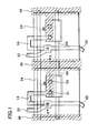
- Fig. 1 is a plan view of a display pixel in an active matrix LCD of a first embodiment of this invention.
- Fig. 2 is a cross-sectional view of the LCD cut along the X-X cross-sectional line shown in Fig. 1.
- the same reference numerals will be given to the same components as in Figs. 9 and 10, and the explanation on those components will be omitted.
- the LCD has a first substrate 100 and a second substrate 500 made of transparent insulating material such as glass, and a liquid crystal 200 placed between the two substrates.
- FIG. 7 An equivalent circuit of each of pixels is shown in Fig. 7.
- Pixel electrodes 24 are disposed in a matrix configuration on the first substrate 100 as seen from Fig. 1.
- a top gate type TFT 1 is placed for each of the pixel electrodes.
- An active layer 14 of the TFT 1 in each of the pixel is in a U-shape and intersects, at two points, a gate line 20, which extends straight in a row direction. At the portion where the active layer and the gate line intersect each other, the active layer 14 makes a channel region 14c, and the gate line 20 becomes the gate.
- a gate insulating layer 66 is formed between the gate and the channel region 14c.
- a drain 14d of the active layer 14 is connected to a data line 22 extending in a column direction through a contact hole made in an interlayer insulating layer 68 and the gate insulating layer 66.
- a source 14s of the active layer 14 is connected to a supplemental pixel electrode 40 through a contact hole C1 made in the interlayer insulating layer 68 and the gate insulating layer 66.
- the supplemental pixel electrode 40 is disposed in the same layer (for example, an aluminum layer) as the data line 22 on the interlayer insulating layer 68 and extends over the region between the pixels adjacent to each other in the row direction. That is, the supplemental pixel electrode 40 extends to cover the area between the pixel electrodes 24, of the pixel adjacent to each other. Additionally, the supplemental pixel electrode 40 is connected to the pixel electrode 24 (a reflecting electrode) on the upper layer through a contact hole C2 made in a flattening insulating layer 72.
- a storage capacitance line 84 is configured in the same layer (for example, molybdenum film, chrome film) as the gate line 20, and extends in a row direction.
- the storage capacitance line 84 is overlapped with a part of the active layer 14 through the gate insulating layer 66. This overlapped part forms a storage capacitance element.
- the supplemental pixel electrode 40 enables the area between the pixels to be utilized as a part of the display region. Since the same voltage applied to the pixel electrode 24 through the top gate type TFT 1 also drives the liquid crystal in the area between the pixels, this area will not show white light, thus improving the display quality.
- Fig. 3 is a cross-sectional view of a display pixel in an active matrix LCD of a second embodiment of this invention. This figure shows a cross section of the device corresponding to the cross section of Fig. 2.
- the planar configuration of the device of this embodiment is substantially the same as that of Fig. 2 except the cut in the insulating layer 72 as described below.
- the thick flattening insulating layer 72 on the supplemental pixel electrode 40 extending over the area between the pixel electrodes 24, adjacent to each other.
- the liquid crystal 200 is placed on the flattening insulating layer 72.
- the insulating layer is placed between the electrode and the liquid crystal, an electric charge is accumulated in this part, resulting in burning of the liquid crystal.
- the thick flattening insulating layer 72 on the supplemental pixel electrode 40 is removed, as seen from Fig. 3, in this embodiment.
- etching can be performed to expose the supplemental pixel electrode 40 by using the pixel electrodes 24, as masks. This prevents the burning of the liquid crystal and improves the display quality.
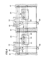
- Fig. 4 is a plan view of a display pixel in an active matrix LCD of a third embodiment of this invention.
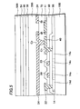
- Fig. 5 is a cross-sectional view of the LCD cut along the X-X cross-sectional line shown in Fig. 4. Again, the same reference numerals are used to indicate the same components. The explanation on these components will be omitted.
- the portion of the supplemental pixel electrode 40 extending over the area between the adjacent pixels of Fig. 1 is cut off from the remaining portion of the supplemental electrode 40.
- the cut-off portion becomes a floating electrode 41 of this embodiment and forms a capacity coupling with each of the pixel electrodes 24, 24 of the adjacent pixels through the flattening insulating layer 72.
- the voltage of the supplemental pixel electrode 40 is the same voltage as the pixel electrode 24 in the first embodiment, as the supplemental pixel electrode 40 is connected to the pixel electrode 24 of one of the pixels. However, since the floating electrode 41 is electrically floating, the voltage is determined by the voltage of the pixel electrode 24, with which the floating electrode 40 forms the capacity coupling. That is, the voltage is determined based on the capacitance of the pixel electrode 24 and the floating electrode 41, and the capacity coupling of these two electrodes.
- the voltage corresponding to that of these two pixel electrodes 24, (the voltage corresponding to black display) is applied to the floating electrode 41, resulting in substantially similar black representation at the area between the adjacent pixels.
- the voltage corresponding to black display is applied to the floating electrode 41, resulting in substantially similar black representation at the area between the adjacent pixels.
- a voltage between the black display and the white display is applied to the floating electrode 41, resulting in a gray representation.
- the voltage of the floating electrodes 41 changes along with the voltage change of the pixel electrodes 24.
- the alignment of the liquid crystal 200 on the floating electrode 41 is also determined by the voltage change of the pixel electrodes 24, eliminating the conventional problems of the conventional device.
- the floating electrode 41 of this embodiment is configured by cutting off a portion of the supplemental pixel electrode 40 of the first embodiment.
- the floating electrode 41 can also be configured by using a different layer.
- the floating electrode 41 equally overlaps the pixel electrodes 24, located at the both sides. However, it is possible to make the induced voltage of the floating electrode 41 be controlled substantially by the voltage of one of the pixel electrodes by disposing the floating electrode 41 substantially toward that pixel electrode to overlap more with that pixel electrode than the other electrode. This configuration is suitable for displaying letters and drawing, which requires clear-cut boundary.
- Fig. 6 is a cross-sectional view of a display pixel in an active matrix LCD of a forth embodiment of this invention. This figure shows a cross section of the device corresponding to the cross section of Fig. 4.
- the planar configuration of the device of this embodiment is substantially the same as that of Fig. 4 except the cut in the insulating layer 72 as described below.
- the thick flattening insulating layer 72 on the floating electrode 41 of the third embodiment is removed in this embodiment.
- the etching is performed to expose the floating electrode 41 by using, for example, the pixel electrodes 24, as masks. This prevents the burning of the liquid crystal 200 and improves the display quality, for the same reason as the second embodiment.
- the supplemental pixel electrode which is connected to the pixel electrode of one of the adjacent pixels and which extends to the area between the adjacent pixels, is disposed in the active matrix LCD of this invention, enabling the area between the pixels to be used as a part of the display area.
- this area does not show white light when the pixel displays black, leading to the improved display quality.
- the floating electrode which forms a capacity coupling at the both pixel electrodes of the pixels adjacent to each other through the insulating layer, is disposed.
- the voltage of the floating electrode changes in accordance with the voltage change of the pixel electrode. Since the voltage similar to that of the pixel region also drives the liquid crystal in the area between the pixels of the LCD, the region will not show white light when the pixel displays black.
Landscapes
- Physics & Mathematics (AREA)
- Nonlinear Science (AREA)
- Engineering & Computer Science (AREA)
- Mathematical Physics (AREA)
- Chemical & Material Sciences (AREA)
- Crystallography & Structural Chemistry (AREA)
- General Physics & Mathematics (AREA)
- Optics & Photonics (AREA)
- Power Engineering (AREA)
- Microelectronics & Electronic Packaging (AREA)
- Liquid Crystal (AREA)
- Devices For Indicating Variable Information By Combining Individual Elements (AREA)
Abstract
Description
Claims (9)
- An active matrix display device comprising:wherein the supplemental pixel electrode (40) extends to and covers a region between the corresponding pixel and the pixel that is next to said corresponding pixel.a plurality of pixels;a thin film transistor provided for each of the pixels;a pixel electrode (24) provided for each of the pixels; anda supplemental pixel electrode (40) provided for each of the pixels and connected to the corresponding pixel electrode,
- The active matrix display device of claim 1, wherein a part of the supplemental pixel electrode (40) is disposed under the corresponding pixel electrode (24) with an insulating layer (72) disposed between the supplemental pixel electrode (40) and the corresponding pixel electrode (24).
- The active matrix display device of claim 2, wherein the supplemental pixel electrode (40) is connected to a source (14s) of the corresponding thin film transistor and to the corresponding pixel electrode (24) that is disposed above the supplemental pixel electrode (40).
- The active matrix display device of claim 2, wherein a portion of the insulating layer (72) disposed on the supplemental pixel electrode (40) is removed.
- An active matrix display device comprising:a plurality of pixels;a thin film transistor provided for each of the pixels;a pixel electrode (24) provided for each of the pixels;a floating electrode (41) disposed to cover a region between two adjacent pixels and forming a capacity coupling with each of the pixel electrodes (24) of the two adjacent pixels; andan insulating layer (72) disposed between the floating electrode and the two corresponding pixel electrodes.
- The active matrix display device of claim 5, wherein the floating electrode (41) is disposed partially under the corresponding pixel electrodes (24).
- The active matrix display device of claim 6, a portion of the insulating layer (72) disposed on the floating electrode (41) is removed.
- An active matrix display device according to any of the claims 1 to 7, wherein the supplementary electrode (40, 41) is arranged in the same layer as a data line (22) connected to the thin film transistor.
- An active matrix display device comprising:two pixels that are disposed adjacent to each other;two pixel electrodes (24) provided for the two pixels;a gap electrode (41) covering more than a half of the entire region between the two pixels and disposed underneath the two pixel electrodes (24); andan insulating layer (72) disposed between the gap electrode (41) and the two pixel electrodes (24).
Applications Claiming Priority (2)
| Application Number | Priority Date | Filing Date | Title |
|---|---|---|---|
| JP2002004777A JP2003207794A (en) | 2002-01-11 | 2002-01-11 | Active matrix display |
| JP2002004777 | 2002-01-11 |
Publications (2)
| Publication Number | Publication Date |
|---|---|
| EP1329764A2 true EP1329764A2 (en) | 2003-07-23 |
| EP1329764A3 EP1329764A3 (en) | 2005-01-19 |
Family
ID=19191030
Family Applications (1)
| Application Number | Title | Priority Date | Filing Date |
|---|---|---|---|
| EP03000723A Withdrawn EP1329764A3 (en) | 2002-01-11 | 2003-01-13 | Active matrix display device |
Country Status (6)
| Country | Link |
|---|---|
| US (2) | US6999149B2 (en) |
| EP (1) | EP1329764A3 (en) |
| JP (1) | JP2003207794A (en) |
| KR (1) | KR100483095B1 (en) |
| CN (1) | CN1220105C (en) |
| TW (1) | TW584757B (en) |
Cited By (2)
| Publication number | Priority date | Publication date | Assignee | Title |
|---|---|---|---|---|
| RU2439639C1 (en) * | 2008-02-21 | 2012-01-10 | Шарп Кабусики Кайся | Active matrix base and liquid-crystal display |
| US9305496B2 (en) | 2010-07-01 | 2016-04-05 | Semiconductor Energy Laboratory Co., Ltd. | Electric field driving display device |
Families Citing this family (13)
| Publication number | Priority date | Publication date | Assignee | Title |
|---|---|---|---|---|
| JP4149168B2 (en) | 2001-11-09 | 2008-09-10 | 株式会社半導体エネルギー研究所 | Light emitting device |
| KR100882729B1 (en) * | 2003-05-14 | 2009-02-06 | 엘지디스플레이 주식회사 | Liquid Crystal Display and Manufacturing Method Thereof |
| US7397067B2 (en) | 2003-12-31 | 2008-07-08 | Intel Corporation | Microdisplay packaging system |
| CN100397442C (en) * | 2004-05-28 | 2008-06-25 | 鸿富锦精密工业(深圳)有限公司 | Active Matrix Display Device |
| KR20060118208A (en) * | 2005-05-16 | 2006-11-23 | 삼성전자주식회사 | Thin film transistor array panel |
| TWI320602B (en) | 2006-03-23 | 2010-02-11 | Prime View Int Co Ltd | E-ink display and method for repairing the same |
| CN101174639B (en) * | 2006-10-31 | 2010-05-19 | 元太科技工业股份有限公司 | Electronic ink display device and repairing method thereof |
| CN101174638B (en) * | 2006-10-31 | 2010-05-19 | 元太科技工业股份有限公司 | Electronic ink display device and repairing method thereof |
| KR101442147B1 (en) * | 2008-01-30 | 2014-11-03 | 삼성디스플레이 주식회사 | Liquid crystal display |
| JP5505442B2 (en) * | 2010-02-15 | 2014-05-28 | カシオ計算機株式会社 | Display device and camera |
| TWI417627B (en) * | 2010-12-24 | 2013-12-01 | 友達光電股份有限公司 | Pixel structure |
| KR102461212B1 (en) * | 2016-02-17 | 2022-11-01 | 티씨엘 차이나 스타 옵토일렉트로닉스 테크놀로지 컴퍼니 리미티드 | Display device and method for fabricating the same |
| CN110741428B (en) * | 2018-02-28 | 2021-12-21 | 京瓷株式会社 | Display device, glass substrate, and method for manufacturing glass substrate |
Family Cites Families (22)
| Publication number | Priority date | Publication date | Assignee | Title |
|---|---|---|---|---|
| US3844637A (en) * | 1973-08-29 | 1974-10-29 | Bunker Ramo | Integrated liquid crystal luminophor display |
| JPS59123875A (en) | 1982-12-28 | 1984-07-17 | セイコーエプソン株式会社 | Liquid crystal display |
| JPH02245741A (en) | 1989-03-17 | 1990-10-01 | Matsushita Electric Ind Co Ltd | Reflection type liquid crystal display device |
| DE69230138T2 (en) * | 1991-11-29 | 2000-04-27 | Seiko Epson Corp., Tokio/Tokyo | LIQUID CRYSTAL DISPLAY DEVICE AND METHOD FOR PRODUCING THE SAME |
| JPH0695144A (en) | 1992-09-10 | 1994-04-08 | Hosiden Corp | Liquid crystal display element |
| TW347477B (en) * | 1994-09-30 | 1998-12-11 | Sanyo Electric Co | Liquid crystal display with storage capacitors for holding electric charges |
| JP3143591B2 (en) * | 1995-09-14 | 2001-03-07 | キヤノン株式会社 | Display device |
| JP3049689B2 (en) * | 1995-09-14 | 2000-06-05 | キヤノン株式会社 | Liquid crystal display |
| JP3272212B2 (en) * | 1995-09-29 | 2002-04-08 | シャープ株式会社 | Transmissive liquid crystal display device and method of manufacturing the same |
| JP3126661B2 (en) | 1996-06-25 | 2001-01-22 | 株式会社半導体エネルギー研究所 | Liquid crystal display |
| JPH1039336A (en) | 1996-07-26 | 1998-02-13 | Toshiba Corp | Active matrix type liquid crystal display |
| JP3634089B2 (en) | 1996-09-04 | 2005-03-30 | 株式会社半導体エネルギー研究所 | Display device |
| JP3739523B2 (en) | 1997-04-16 | 2006-01-25 | 富士写真フイルム株式会社 | Reflective two-dimensional matrix spatial light modulator |
| US6330047B1 (en) * | 1997-07-28 | 2001-12-11 | Sharp Kabushiki Kaisha | Liquid crystal display device and method for fabricating the same |
| JP3980156B2 (en) | 1998-02-26 | 2007-09-26 | 株式会社半導体エネルギー研究所 | Active matrix display device |
| JP4180690B2 (en) * | 1998-06-05 | 2008-11-12 | 東芝松下ディスプレイテクノロジー株式会社 | Liquid crystal display |
| KR100430773B1 (en) * | 1998-07-14 | 2004-05-10 | 가부시끼가이샤 도시바 | Active matrix type liquid crystal displ ay |
| JP3401589B2 (en) * | 1998-10-21 | 2003-04-28 | 株式会社アドバンスト・ディスプレイ | TFT array substrate and liquid crystal display |
| US6356327B1 (en) * | 1999-03-29 | 2002-03-12 | National Semiconductor Corporation | Pixel array for silicon LC light valve featuring reflective metal surface underlying inter-pixel regions |
| KR100675088B1 (en) * | 2000-02-16 | 2007-01-26 | 엘지.필립스 엘시디 주식회사 | Liquid crystal display and liquid crystal display manufacturing method |
| TWI301915B (en) * | 2000-03-17 | 2008-10-11 | Seiko Epson Corp | |
| JP3823016B2 (en) | 2000-07-21 | 2006-09-20 | 株式会社日立製作所 | Liquid crystal display |
-
2002
- 2002-01-11 JP JP2002004777A patent/JP2003207794A/en active Pending
- 2002-09-04 TW TW091120131A patent/TW584757B/en not_active IP Right Cessation
- 2002-10-31 CN CNB021459878A patent/CN1220105C/en not_active Expired - Lifetime
-
2003
- 2003-01-09 KR KR10-2003-0001328A patent/KR100483095B1/en not_active Expired - Lifetime
- 2003-01-10 US US10/339,647 patent/US6999149B2/en not_active Expired - Lifetime
- 2003-01-13 EP EP03000723A patent/EP1329764A3/en not_active Withdrawn
-
2005
- 2005-11-29 US US11/288,251 patent/US7248322B2/en not_active Expired - Fee Related
Cited By (3)
| Publication number | Priority date | Publication date | Assignee | Title |
|---|---|---|---|---|
| RU2439639C1 (en) * | 2008-02-21 | 2012-01-10 | Шарп Кабусики Кайся | Active matrix base and liquid-crystal display |
| US9305496B2 (en) | 2010-07-01 | 2016-04-05 | Semiconductor Energy Laboratory Co., Ltd. | Electric field driving display device |
| US10274803B2 (en) | 2010-07-01 | 2019-04-30 | Semiconductor Energy Laboratory Co., Ltd. | Electric field driving display device |
Also Published As
| Publication number | Publication date |
|---|---|
| EP1329764A3 (en) | 2005-01-19 |
| US20060077331A1 (en) | 2006-04-13 |
| US20030136962A1 (en) | 2003-07-24 |
| US7248322B2 (en) | 2007-07-24 |
| CN1431547A (en) | 2003-07-23 |
| KR100483095B1 (en) | 2005-04-14 |
| JP2003207794A (en) | 2003-07-25 |
| CN1220105C (en) | 2005-09-21 |
| TW584757B (en) | 2004-04-21 |
| US6999149B2 (en) | 2006-02-14 |
| KR20030061320A (en) | 2003-07-18 |
Similar Documents
| Publication | Publication Date | Title |
|---|---|---|
| US7830477B2 (en) | Liquid crystal display device | |
| KR100250093B1 (en) | Active Matrix Substrate and Manufacturing Method Thereof | |
| US6252248B1 (en) | Thin film transistor and display | |
| US8259248B2 (en) | Electrooptic device and electronic device | |
| US7248322B2 (en) | Active matrix display device with floating electrode between adjacent pixels | |
| US6819385B2 (en) | Transflective pixel structure | |
| JPH09203908A (en) | Thin film transistor for liquid crystal display device and liquid crystal display device | |
| EP1956426A1 (en) | Display substrate, display apparatus having the same and method of manufacturing the display substrate | |
| KR0123445B1 (en) | LCD Display | |
| EP2571059A1 (en) | Semiconductor device, active matrix substrate, and display device | |
| US20230205020A1 (en) | Display device | |
| JP4141892B2 (en) | Pixel structure of thin film transistor liquid crystal display | |
| US8017947B2 (en) | Thin film transistor array panel, display device including the same, and method thereof | |
| KR20060107929A (en) | Electro-optical device and its manufacturing method, and electronic device | |
| JP2003279944A (en) | Liquid crystal display | |
| US7573539B2 (en) | Liquid crystal display apparatus | |
| JP2007213003A (en) | ELECTRO-OPTICAL DEVICE, MANUFACTURING METHOD THEREOF, AND ELECTRONIC DEVICE | |
| JP4245008B2 (en) | Electro-optical device substrate, electro-optical device, and electronic apparatus | |
| JP3733769B2 (en) | Liquid crystal device | |
| KR100806891B1 (en) | Thin film transistor substrate for liquid crystal display | |
| JP2002297058A (en) | Active matrix display | |
| JP2002296619A (en) | Active matrix display | |
| US20060087609A1 (en) | Liquid crystal display device | |
| JP2007192975A (en) | Electro-optical device and manufacturing method thereof | |
| US12353103B2 (en) | Display device |
Legal Events
| Date | Code | Title | Description |
|---|---|---|---|
| PUAI | Public reference made under article 153(3) epc to a published international application that has entered the european phase |
Free format text: ORIGINAL CODE: 0009012 |
|
| AK | Designated contracting states |
Designated state(s): AT BE BG CH CY CZ DE DK EE ES FI FR GB GR HU IE IT LI LU MC NL PT SE SI SK TR |
|
| AX | Request for extension of the european patent |
Extension state: AL LT LV MK RO SI |
|
| PUAL | Search report despatched |
Free format text: ORIGINAL CODE: 0009013 |
|
| AK | Designated contracting states |
Kind code of ref document: A3 Designated state(s): AT BE BG CH CY CZ DE DK EE ES FI FR GB GR HU IE IT LI LU MC NL PT SE SI SK TR |
|
| AX | Request for extension of the european patent |
Extension state: AL LT LV MK RO |
|
| 17P | Request for examination filed |
Effective date: 20050506 |
|
| 17Q | First examination report despatched |
Effective date: 20050613 |
|
| AKX | Designation fees paid |
Designated state(s): DE FI FR GB NL |
|
| STAA | Information on the status of an ep patent application or granted ep patent |
Free format text: STATUS: THE APPLICATION IS DEEMED TO BE WITHDRAWN |
|
| 18D | Application deemed to be withdrawn |
Effective date: 20080610 |