EP1323031B1 - Single instruction multiple data processing - Google Patents
Single instruction multiple data processing Download PDFInfo
- Publication number
- EP1323031B1 EP1323031B1 EP01960902.3A EP01960902A EP1323031B1 EP 1323031 B1 EP1323031 B1 EP 1323031B1 EP 01960902 A EP01960902 A EP 01960902A EP 1323031 B1 EP1323031 B1 EP 1323031B1
- Authority
- EP
- European Patent Office
- Prior art keywords
- data word
- circuit
- instruction
- portions
- data
- Prior art date
- Legal status (The legal status is an assumption and is not a legal conclusion. Google has not performed a legal analysis and makes no representation as to the accuracy of the status listed.)
- Expired - Lifetime
Links
Images
Classifications
-
- G—PHYSICS
- G06—COMPUTING OR CALCULATING; COUNTING
- G06F—ELECTRIC DIGITAL DATA PROCESSING
- G06F7/00—Methods or arrangements for processing data by operating upon the order or content of the data handled
- G06F7/38—Methods or arrangements for performing computations using exclusively denominational number representation, e.g. using binary, ternary, decimal representation
- G06F7/48—Methods or arrangements for performing computations using exclusively denominational number representation, e.g. using binary, ternary, decimal representation using non-contact-making devices, e.g. tube, solid state device; using unspecified devices
- G06F7/50—Adding; Subtracting
- G06F7/505—Adding; Subtracting in bit-parallel fashion, i.e. having a different digit-handling circuit for each denomination
-
- G—PHYSICS
- G06—COMPUTING OR CALCULATING; COUNTING
- G06F—ELECTRIC DIGITAL DATA PROCESSING
- G06F9/00—Arrangements for program control, e.g. control units
- G06F9/06—Arrangements for program control, e.g. control units using stored programs, i.e. using an internal store of processing equipment to receive or retain programs
- G06F9/30—Arrangements for executing machine instructions, e.g. instruction decode
- G06F9/30003—Arrangements for executing specific machine instructions
- G06F9/30007—Arrangements for executing specific machine instructions to perform operations on data operands
- G06F9/3001—Arithmetic instructions
- G06F9/30014—Arithmetic instructions with variable precision
-
- G—PHYSICS
- G06—COMPUTING OR CALCULATING; COUNTING
- G06F—ELECTRIC DIGITAL DATA PROCESSING
- G06F9/00—Arrangements for program control, e.g. control units
- G06F9/06—Arrangements for program control, e.g. control units using stored programs, i.e. using an internal store of processing equipment to receive or retain programs
- G06F9/30—Arrangements for executing machine instructions, e.g. instruction decode
- G06F9/30003—Arrangements for executing specific machine instructions
- G06F9/30007—Arrangements for executing specific machine instructions to perform operations on data operands
- G06F9/30025—Format conversion instructions, e.g. Floating-Point to Integer, decimal conversion
-
- G—PHYSICS
- G06—COMPUTING OR CALCULATING; COUNTING
- G06F—ELECTRIC DIGITAL DATA PROCESSING
- G06F9/00—Arrangements for program control, e.g. control units
- G06F9/06—Arrangements for program control, e.g. control units using stored programs, i.e. using an internal store of processing equipment to receive or retain programs
- G06F9/30—Arrangements for executing machine instructions, e.g. instruction decode
- G06F9/30003—Arrangements for executing specific machine instructions
- G06F9/30007—Arrangements for executing specific machine instructions to perform operations on data operands
- G06F9/30032—Movement instructions, e.g. MOVE, SHIFT, ROTATE, SHUFFLE
-
- G—PHYSICS
- G06—COMPUTING OR CALCULATING; COUNTING
- G06F—ELECTRIC DIGITAL DATA PROCESSING
- G06F9/00—Arrangements for program control, e.g. control units
- G06F9/06—Arrangements for program control, e.g. control units using stored programs, i.e. using an internal store of processing equipment to receive or retain programs
- G06F9/30—Arrangements for executing machine instructions, e.g. instruction decode
- G06F9/30003—Arrangements for executing specific machine instructions
- G06F9/30007—Arrangements for executing specific machine instructions to perform operations on data operands
- G06F9/30036—Instructions to perform operations on packed data, e.g. vector, tile or matrix operations
- G06F9/30038—Instructions to perform operations on packed data, e.g. vector, tile or matrix operations using a mask
-
- G—PHYSICS
- G06—COMPUTING OR CALCULATING; COUNTING
- G06F—ELECTRIC DIGITAL DATA PROCESSING
- G06F2207/00—Indexing scheme relating to methods or arrangements for processing data by operating upon the order or content of the data handled
- G06F2207/38—Indexing scheme relating to groups G06F7/38 - G06F7/575
- G06F2207/3804—Details
- G06F2207/3808—Details concerning the type of numbers or the way they are handled
- G06F2207/3828—Multigauge devices, i.e. capable of handling packed numbers without unpacking them
-
- G—PHYSICS
- G06—COMPUTING OR CALCULATING; COUNTING
- G06F—ELECTRIC DIGITAL DATA PROCESSING
- G06F7/00—Methods or arrangements for processing data by operating upon the order or content of the data handled
- G06F7/38—Methods or arrangements for performing computations using exclusively denominational number representation, e.g. using binary, ternary, decimal representation
- G06F7/48—Methods or arrangements for performing computations using exclusively denominational number representation, e.g. using binary, ternary, decimal representation using non-contact-making devices, e.g. tube, solid state device; using unspecified devices
- G06F7/499—Denomination or exception handling, e.g. rounding or overflow
- G06F7/49931—Modulo N reduction of final result
Definitions
- This invention relates to the field of data processing systems. More particularly, this invention relates to data processing system in which it is desired to provide single instruction multiple data type operation.
- Single instruction multiple data operation is a known technique whereby data words being manipulated in accordance with a single instruction in fact represent multiple data values within those data words with the manipulation specified being independently performed upon respective data values.
- This type of instruction can increase the efficiency with which a data processing system may operate and is particularly useful in reducing code size and speeding up processing operation.
- the technique is commonly, but not exclusively, applied to the field of manipulating data values representing physical signals, such as in digital signal processing applications.
- US 6 061 783-A discloses a method and apparatus for direct manipulation of bit fields contained in a memory source.
- An ADD or SUBTRACT operation is performed on a temporary destination argument produced form an initial destination argument by masking off bits and padding the masked off bits with either 1's or 0's or a combination of 1's and 0's depending on the operation taking place to form a 64-bit argument.
- the ADD operation only modifies the bit field [15:8] of the temporary destination argument with the remaining bits of data not associated with the bit field remaining unchanged.
- EP 0 945 783-A discloses a variable length register device having an operational instruction that arithmetically adds data in an nth B3 area in the variable length register of a source A to data in the mth H0 area of the variable length register of a source B.
- US-A-6 081 824 discloses a standard SIMD instruction which performs corresponding SIMD arithmetic instructions in each lane.
- the present invention provides apparatus for data processing as defined in claim 1.
- the invention provides a new data processing instruction within a data processing system that may serve to unpack data values held within a data word and also perform a single-instruction-multiple-data type arithmetic operation upon the unpacked data values.
- the invention recognises that by unpacking non-adjacent data values within a data word may be implemented with considerably less additional overhead than conventional unpacking instructions which unpack adjacent data values. In particular, the need for additional data pathways that can diverge the bit positions of previously adjacent data values may be avoided. Instead, for example, already present masking and word shifting circuitry may be utilised. Furthermore, the simplification of the unpacking function allows the possibility for a single instructions to also provide an arithmetic operation upon the operands without introducing processing cycle constraint problems.
- the invention may be applied to the selection of nonadjacent multibit portions of arbitrary length compared to their promoted length, particularly efficient and convenient implementations are ones in which the selected multibit portions are half the length of the promoted multibit portions with the promoted multibit portions being abutted within a promoted data word so as to have a length equal to the length of the input data words to the operation.
- arithmetic operation that is combined with the unpacking could take various different forms. However, particularly preferred embodiments are ones in which the arithmetic operation is an add operation performed independently upon respective promoted multibit portions. This instruction is particularly useful in many real life data processing situations, such as during the calculation of a sum of absolute differences as part of MPEG motion compensation calculations.
- the invention is able to make use of existing processing resources within a data processing system in a more effective manner. This is particularly the case in a system in which a shifting circuit is provided upstream of an arithmetic circuit within the data path. Such an arrangement allows the unpacking, with any of the optional shifts, to be performed prior to an arithmetic operation.
- a promoting circuit that is responsible for promoting the selected multibit portions in length (e. g. either by sign extension or leading zero extension) is provided in parallel with a portion of the shifting circuit and the range of common shift amounts that is specified is restricted such that a first part of the shifting circuit can be used in combination with the promoting circuit to perform the required operations without extending the time data value takes to propagate beyond that already allowed for to provide propagation through the full shifting circuit in other operations.
- the invention provides a method as defined in claim 12.
- the invention also provides a computer program product as defined in claim 13.
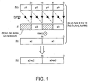
- Figure 1 illustrates the action of a first SIMD type data processing instruction termed ADD8TO16 according to an embodiment of the invention.
- This instruction comes in both signed and unsigned variants corresponding to the nature of the extension added to the front of a selected portion of each of the input operand data words as it is extended in length as part of the processing performed.
- the first input operand data word is stored within a register Rm of the data processing apparatus.
- the data word is formed of four 8-bit portions p0, p1, p2 and p3. Depending upon whether or not a rotate right operation of 8-bit positions is specified in the instruction, either the multibit portions p0 and p2 or alternatively the multibit portions p1 and p3 are selected out of the input data word within register Rm.
- the optional rotate right operation may also be by amounts of 16 and 24 if desired. This effectively allows the high and low order portions to be swapped around.
- the example illustrated in Figure 1 shows the non-adjacent portions p0 and p2 being selected in the unrotated (shifted) variant with the other variant being indicated by the dotted lines.
- each is promoted in length from 8 bits to 16 bits using either zero or sign extension.
- the shaded portions of the promoted data word P shown in Figure indicate these extension portions.
- the second input data word is stored within a register Rn and comprises two 16-bit data values.
- the example illustrated performs a single-instruction-multiple-data add operation whereby the extended p0 value is added to the lower 16 bit value a0 of Rn whilst the extended p2 value is added to the upper 16 bit portion a2 of the Rn value.
- This type of addition is one which may be considered as a full width addition with the carry chain broken between the 15th and 16th bits of the result. It will be appreciated that other SIMD type arithmetic operations may be performed, such as, for example, a SIMD subtraction.
- the output result data word generated by the instruction of Figure 1 produces in the lower 16 bits the sum of p0 and a0 whilst the upper 16 bits contain the sum of p2 and a2.
- This instruction is particularly useful in operations that determine the sum of absolute differences between respective data values whereby the a0 and a2 represent accumulate values with the values p0 to p3 representing individual absolute values of signal difference values, such as pixel difference values. This type of operation is commonly needed in MPEG motion estimation processing and the ability to perform this operation at high speed is strongly advantageous.
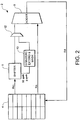
- Figure 2 illustrates an example data path 2 of a data processing system according to an embodiment of the invention that may be used to implement the instruction of Figure 1 .
- a register bank 4 holds 32-bit data words to be manipulated. Both the input operand data words stored in Rm and Rn are read from this register bank and the result data word is written back to register Rd in the register bank 4.
- the data path 2 includes a shifting circuit 6 and an adder circuit 8. The many other data processing instructions provided by the system utilise this shifting circuit 6 and adder circuit 8 in various different ways. Such a data path 2 is carefully designed so that the time taken for a data value to propagate through the shifting circuit 6 and the adder circuit 8 is well matched to the data processing cycle time.
- a sign/zero extending and masking circuit 10 is provided in parallel with lower portion of the shifting circuit 6.
- a multiplex 12 is able to select either the output of the full shifting circuit 6 or the output of the sign/zero extending and masking circuit 10 as one of the inputs to the adder circuit 8.
- the other input to the adder circuit 8 is the input operand data word of Rn.
- the input operand data word of Rm is supplied to the shifting circuit 6 in which an optional right shift of 8-bit positions is applied to the data word in dependence upon whether or not that parameter was specified within the instruction.
- Optional right rotates of 16 and 24 bit positions may also be applied.
- a multilevel multiplexer based shifter such a restricted possibility shift may be provided relatively simply from a first portion of the shifting circuit 6 (e. g. in the case of a 32-bit system the first level of multiplexer may provide 16 bits of shift and the second level of mulitplexer provides 8 bits of shift).
- a value optionally shifted by the specified amount can be tapped off from part way through the shifting circuit 6 and supplied to the sign/zero extending and masking circuit 10.
- This circuit 10 operates to mask out the non-selected multibit portions of the possibly shifted input operand data word of Rm and replace these masked out portions with either zeros or a sign extension of their respective selected multibit portions.
- the output of the sign/zero extending and masking circuit 10 passes via a multiplexer 12 to a first input of the adder circuit 8.
- the second input of the adder circuit 8 is the input operand data word of Rn.
- the adder circuit 8 performs a SIMD add upon its inputs (i. e. two parallel 16-bit adds with the carry chain effectively broken between bit positions 15 and 16).
- the output of the adder circuit 8 is written back into register Rd of the a register bank 4.
- the sign/zero extending and masking circuit 10 may take Rm (unrotated) as its input and then itself perform a rotate of 0,8,16 or 24 upon the four possible sign bits and then create the mask.
- the shifting circuit 6 would operate in parallel to shift the whole 32 bits of Rm.
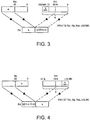
- Figures 3 and 4 illustrate two variants of an illustrative example half word packing SIMD type instruction.
- the PKHTB instruction of Figure 3 takes a fixed top half of one input operand data word stored in register Rn and a variable position half bit portion of a second input operand data word stored in register Rm and combines these into respectively the top half and the bottom half of an output data word to be stored in register Rd.
- the instruction PKHBT takes the bottom half of an input operand data word of Rn and a variable position half word length portion of a second input operand data word of Rm and combines these respectively into the bottom and top halves of an output data word of Rd.
- variable position half word portion of the instruction of Figure 3 is selected from bit positions 15 to 0 of the word of Rm after that word has been right shifted by k bit positions.
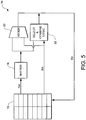
- the half word length variable position portion of Rm selected in accordance with the instruction of Figure 4 is selected from bit positions 31 to 16 of the word of Rm after that word has been left shifted by k bit positions.
- variable shifting provided in combination with the packing function of the instructions of Figure 3 and Figure 4 is particularly useful for adjusting changes in the "Q" value of fixed point arithmetic values that can occur during manipulation of those values.
- Figure 5 illustrates an example data path 14 that is particularly well suited for performing the instructions of Figures 3 and 4 .
- a register bank 16 again provides the input operand data words, being 32-bit data words in this example, and stores the output data word.
- the data path includes a shifting circuit 18, an adder circuit 20 and a selecting and combining circuit 22.
- the unshifted input operand data word of Rn passes directly from the register bank 16 to the selecting and combining logic 22.
- the most significant 16 bits of the value of Rn are selected and form the corresponding bits within the output data word Rd.
- the input operand data word of Rm passes through the full shifting circuit 18.
- the shifting circuit 18 provides a left logical shift of k bit positions and supplies the result to the selecting and combining circuit 22.
- the selecting and combining circuit 22 selects the most significant 16 bits of the output of the shifting circuit 18 and uses these to form the most significant 16 bits of the output data word of Rd.
- the selecting and combining circuit 22 is provided in a position in parallel with the adder circuit 20. Accordingly, given that the data path 14 is carefully designed to allow for a full shift and add operation to be performed within a processing cycle, the relatively straight forward operation of selecting and combining can be provided within the time period normally allowed for the operation of the adder circuit 20 without imposing any processing cycle constraints.
Landscapes
- Engineering & Computer Science (AREA)
- Theoretical Computer Science (AREA)
- Physics & Mathematics (AREA)
- Software Systems (AREA)
- General Physics & Mathematics (AREA)
- General Engineering & Computer Science (AREA)
- Mathematical Analysis (AREA)
- Pure & Applied Mathematics (AREA)
- Computational Mathematics (AREA)
- Mathematical Physics (AREA)
- Mathematical Optimization (AREA)
- Computing Systems (AREA)
- Executing Machine-Instructions (AREA)
- Advance Control (AREA)
Applications Claiming Priority (3)
| Application Number | Priority Date | Filing Date | Title |
|---|---|---|---|
| GB0024311 | 2000-10-04 | ||
| GB0024311A GB2367650B (en) | 2000-10-04 | 2000-10-04 | Single instruction multiple data processing |
| PCT/GB2001/003744 WO2002029553A1 (en) | 2000-10-04 | 2001-08-21 | Single instruction multiple data processing |
Publications (2)
| Publication Number | Publication Date |
|---|---|
| EP1323031A1 EP1323031A1 (en) | 2003-07-02 |
| EP1323031B1 true EP1323031B1 (en) | 2018-11-14 |
Family
ID=9900674
Family Applications (1)
| Application Number | Title | Priority Date | Filing Date |
|---|---|---|---|
| EP01960902.3A Expired - Lifetime EP1323031B1 (en) | 2000-10-04 | 2001-08-21 | Single instruction multiple data processing |
Country Status (11)
| Country | Link |
|---|---|
| US (1) | US6999985B2 (enExample) |
| EP (1) | EP1323031B1 (enExample) |
| JP (1) | JP5133491B2 (enExample) |
| KR (1) | KR100880614B1 (enExample) |
| CN (1) | CN1196998C (enExample) |
| GB (1) | GB2367650B (enExample) |
| IL (2) | IL151395A0 (enExample) |
| MY (1) | MY129332A (enExample) |
| RU (1) | RU2279706C2 (enExample) |
| TW (1) | TW548587B (enExample) |
| WO (1) | WO2002029553A1 (enExample) |
Families Citing this family (16)
| Publication number | Priority date | Publication date | Assignee | Title |
|---|---|---|---|---|
| JP2003114323A (ja) * | 2001-10-04 | 2003-04-18 | Bridgestone Corp | 近赤外線吸収フィルム |
| JP3857614B2 (ja) * | 2002-06-03 | 2006-12-13 | 松下電器産業株式会社 | プロセッサ |
| US20030231660A1 (en) * | 2002-06-14 | 2003-12-18 | Bapiraju Vinnakota | Bit-manipulation instructions for packet processing |
| US8082419B2 (en) | 2004-03-30 | 2011-12-20 | Intel Corporation | Residual addition for video software techniques |
| US7584233B2 (en) * | 2005-06-28 | 2009-09-01 | Qualcomm Incorporated | System and method of counting leading zeros and counting leading ones in a digital signal processor |
| US7840954B2 (en) * | 2005-11-29 | 2010-11-23 | International Business Machines Corporation | Compilation for a SIMD RISC processor |
| US8290095B2 (en) * | 2006-03-23 | 2012-10-16 | Qualcomm Incorporated | Viterbi pack instruction |
| US8493979B2 (en) * | 2008-12-30 | 2013-07-23 | Intel Corporation | Single instruction processing of network packets |
| US8495341B2 (en) * | 2010-02-17 | 2013-07-23 | International Business Machines Corporation | Instruction length based cracking for instruction of variable length storage operands |
| GB2481384B (en) * | 2010-06-21 | 2018-10-10 | Advanced Risc Mach Ltd | Key allocation when tracing data processing systems |
| WO2012134321A1 (en) * | 2011-03-30 | 2012-10-04 | Intel Corporation | Simd integer addition including mathematical operation on masks |
| WO2012137428A1 (ja) * | 2011-04-08 | 2012-10-11 | パナソニック株式会社 | データ処理装置、及びデータ処理方法 |
| US20130113809A1 (en) | 2011-11-07 | 2013-05-09 | Nvidia Corporation | Technique for inter-procedural memory address space optimization in gpu computing compiler |
| CN103092571B (zh) * | 2013-01-10 | 2016-06-22 | 浙江大学 | 支持多种数据类型的单指令多数据算术单元 |
| US20190196787A1 (en) * | 2017-12-21 | 2019-06-27 | Intel Corporation | Apparatus and method for right shifting packed quadwords and extracting packed doublewords |
| KR102182299B1 (ko) * | 2019-07-24 | 2020-11-24 | 에스케이텔레콤 주식회사 | 시프트 연산 장치 및 그의 동작 방법 |
Citations (1)
| Publication number | Priority date | Publication date | Assignee | Title |
|---|---|---|---|---|
| US6081824A (en) * | 1998-03-05 | 2000-06-27 | Intel Corporation | Method and apparatus for fast unsigned integral division |
Family Cites Families (9)
| Publication number | Priority date | Publication date | Assignee | Title |
|---|---|---|---|---|
| US4785393A (en) * | 1984-07-09 | 1988-11-15 | Advanced Micro Devices, Inc. | 32-Bit extended function arithmetic-logic unit on a single chip |
| EP0540150B1 (en) * | 1991-10-29 | 1999-06-02 | Advanced Micro Devices, Inc. | Arithmetic logic unit |
| US5673321A (en) * | 1995-06-29 | 1997-09-30 | Hewlett-Packard Company | Efficient selection and mixing of multiple sub-word items packed into two or more computer words |
| US6237016B1 (en) * | 1995-09-05 | 2001-05-22 | Intel Corporation | Method and apparatus for multiplying and accumulating data samples and complex coefficients |
| US5835782A (en) * | 1996-03-04 | 1998-11-10 | Intel Corporation | Packed/add and packed subtract operations |
| US5812140A (en) * | 1996-09-05 | 1998-09-22 | Adobe Systems Incorporated | Efficient gray tile storage |
| US6061783A (en) * | 1996-11-13 | 2000-05-09 | Nortel Networks Corporation | Method and apparatus for manipulation of bit fields directly in a memory source |
| JPH11272546A (ja) * | 1998-03-23 | 1999-10-08 | Nec Corp | 可変長レジスタ装置 |
| US6338135B1 (en) * | 1998-11-20 | 2002-01-08 | Arm Limited | Data processing system and method for performing an arithmetic operation on a plurality of signed data values |
-
2000
- 2000-10-04 GB GB0024311A patent/GB2367650B/en not_active Expired - Lifetime
-
2001
- 2001-08-21 RU RU2002124769/09A patent/RU2279706C2/ru not_active IP Right Cessation
- 2001-08-21 WO PCT/GB2001/003744 patent/WO2002029553A1/en not_active Ceased
- 2001-08-21 KR KR1020037004621A patent/KR100880614B1/ko not_active Expired - Lifetime
- 2001-08-21 IL IL15139501A patent/IL151395A0/xx unknown
- 2001-08-21 CN CNB01810648XA patent/CN1196998C/zh not_active Expired - Lifetime
- 2001-08-21 EP EP01960902.3A patent/EP1323031B1/en not_active Expired - Lifetime
- 2001-08-21 JP JP2002533059A patent/JP5133491B2/ja not_active Expired - Lifetime
- 2001-08-29 TW TW090121381A patent/TW548587B/zh not_active IP Right Cessation
- 2001-08-30 US US09/941,790 patent/US6999985B2/en not_active Expired - Lifetime
- 2001-09-21 MY MYPI20014440A patent/MY129332A/en unknown
-
2002
- 2002-08-21 IL IL151395A patent/IL151395A/en active IP Right Grant
Patent Citations (1)
| Publication number | Priority date | Publication date | Assignee | Title |
|---|---|---|---|---|
| US6081824A (en) * | 1998-03-05 | 2000-06-27 | Intel Corporation | Method and apparatus for fast unsigned integral division |
Also Published As
| Publication number | Publication date |
|---|---|
| KR100880614B1 (ko) | 2009-01-30 |
| IL151395A0 (en) | 2003-04-10 |
| JP5133491B2 (ja) | 2013-01-30 |
| EP1323031A1 (en) | 2003-07-02 |
| IL151395A (en) | 2009-09-01 |
| US20020040378A1 (en) | 2002-04-04 |
| KR20030066631A (ko) | 2003-08-09 |
| TW548587B (en) | 2003-08-21 |
| RU2002124769A (ru) | 2004-02-20 |
| GB2367650A (en) | 2002-04-10 |
| WO2002029553A1 (en) | 2002-04-11 |
| CN1432151A (zh) | 2003-07-23 |
| CN1196998C (zh) | 2005-04-13 |
| MY129332A (en) | 2007-03-30 |
| RU2279706C2 (ru) | 2006-07-10 |
| GB2367650B (en) | 2004-10-27 |
| GB0024311D0 (en) | 2000-11-15 |
| JP2004511039A (ja) | 2004-04-08 |
| US6999985B2 (en) | 2006-02-14 |
Similar Documents
| Publication | Publication Date | Title |
|---|---|---|
| EP1323031B1 (en) | Single instruction multiple data processing | |
| EP0657803B1 (en) | Three input arithmetic logic unit | |
| US6742012B2 (en) | Apparatus and method for performing multiplication operations | |
| EP0656584B1 (en) | Conditional memory store from a register pair | |
| EP0660227B1 (en) | Three input arithmetic logic unit forming the sum of a first and a second boolean combination of the inputs | |
| JP3578502B2 (ja) | 単一プロセッサにおいて並列データ処理を実行する方法 | |
| EP0657802B1 (en) | Rotation register for orthogonal data transformation | |
| JP3729881B2 (ja) | 並列加算および平均演算を行うための回路およびその方法 | |
| US10409604B2 (en) | Apparatus and method for performing multiply-and-accumulate-products operations | |
| US5802339A (en) | Pipeline throughput via parallel out-of-order execution of adds and moves in a supplemental integer execution unit | |
| KR19980041798A (ko) | 영상처리를 위한 명령을 지원하는 모듈 계산구조 | |
| EP0478745A1 (en) | High performance interlock collapsing scism alu apparatus | |
| EP0368826A2 (en) | Data processing circuit | |
| US20020026570A1 (en) | SIMD operation system capable of designating plural registers | |
| WO2002029552A1 (en) | Single instruction multiple data processing | |
| EP1634163B1 (en) | Result partitioning within simd data processing systems | |
| US20250130808A1 (en) | Vector transformation in parallel with arithmetic operation | |
| US5235539A (en) | Method and apparatus for generating carry out signals | |
| EP0660223B1 (en) | Three input arithmetic logic unit with barrel rotator | |
| EP0508627B1 (en) | Method and apparatus for generating carry out signals | |
| US7580968B2 (en) | Processor with scaled sum-of-product instructions | |
| GB2367659A (en) | SIMD saturation instruction with variable bit length | |
| JPH087082A (ja) | バレル回転子及びマスク発生器を有する3入力算術論理装置 | |
| JPH08161460A (ja) | 第1の入力に加算された第2の入力と第3の入力との第1のブール組合せプラス第2の入力と第3の入力の第2のブール組合せの和を形成する3入力算術論理装置 |
Legal Events
| Date | Code | Title | Description |
|---|---|---|---|
| PUAI | Public reference made under article 153(3) epc to a published international application that has entered the european phase |
Free format text: ORIGINAL CODE: 0009012 |
|
| 17P | Request for examination filed |
Effective date: 20020814 |
|
| AK | Designated contracting states |
Designated state(s): AT BE CH CY DE DK ES FI FR GB GR IE IT LI LU MC NL PT SE TR |
|
| RBV | Designated contracting states (corrected) |
Designated state(s): DE FR GB IT NL |
|
| 17Q | First examination report despatched |
Effective date: 20071227 |
|
| STAA | Information on the status of an ep patent application or granted ep patent |
Free format text: STATUS: EXAMINATION IS IN PROGRESS |
|
| REG | Reference to a national code |
Ref country code: DE Ref legal event code: R079 Ref document number: 60151003 Country of ref document: DE Free format text: PREVIOUS MAIN CLASS: G06F0009302000 Ipc: G06F0009300000 |
|
| GRAP | Despatch of communication of intention to grant a patent |
Free format text: ORIGINAL CODE: EPIDOSNIGR1 |
|
| STAA | Information on the status of an ep patent application or granted ep patent |
Free format text: STATUS: GRANT OF PATENT IS INTENDED |
|
| RIC1 | Information provided on ipc code assigned before grant |
Ipc: G06F 7/505 20060101ALI20180514BHEP Ipc: G06F 9/30 19800101AFI20180514BHEP |
|
| INTG | Intention to grant announced |
Effective date: 20180606 |
|
| GRAS | Grant fee paid |
Free format text: ORIGINAL CODE: EPIDOSNIGR3 |
|
| GRAA | (expected) grant |
Free format text: ORIGINAL CODE: 0009210 |
|
| STAA | Information on the status of an ep patent application or granted ep patent |
Free format text: STATUS: THE PATENT HAS BEEN GRANTED |
|
| AK | Designated contracting states |
Kind code of ref document: B1 Designated state(s): DE FR GB IT NL |
|
| REG | Reference to a national code |
Ref country code: GB Ref legal event code: FG4D |
|
| REG | Reference to a national code |
Ref country code: DE Ref legal event code: R096 Ref document number: 60151003 Country of ref document: DE |
|
| REG | Reference to a national code |
Ref country code: NL Ref legal event code: MP Effective date: 20181114 |
|
| PG25 | Lapsed in a contracting state [announced via postgrant information from national office to epo] |
Ref country code: NL Free format text: LAPSE BECAUSE OF FAILURE TO SUBMIT A TRANSLATION OF THE DESCRIPTION OR TO PAY THE FEE WITHIN THE PRESCRIBED TIME-LIMIT Effective date: 20181114 |
|
| PG25 | Lapsed in a contracting state [announced via postgrant information from national office to epo] |
Ref country code: IT Free format text: LAPSE BECAUSE OF FAILURE TO SUBMIT A TRANSLATION OF THE DESCRIPTION OR TO PAY THE FEE WITHIN THE PRESCRIBED TIME-LIMIT Effective date: 20181114 |
|
| REG | Reference to a national code |
Ref country code: DE Ref legal event code: R097 Ref document number: 60151003 Country of ref document: DE |
|
| PLBE | No opposition filed within time limit |
Free format text: ORIGINAL CODE: 0009261 |
|
| STAA | Information on the status of an ep patent application or granted ep patent |
Free format text: STATUS: NO OPPOSITION FILED WITHIN TIME LIMIT |
|
| 26N | No opposition filed |
Effective date: 20190815 |
|
| PGFP | Annual fee paid to national office [announced via postgrant information from national office to epo] |
Ref country code: GB Payment date: 20200722 Year of fee payment: 20 Ref country code: FR Payment date: 20200721 Year of fee payment: 20 Ref country code: DE Payment date: 20200721 Year of fee payment: 20 |
|
| REG | Reference to a national code |
Ref country code: DE Ref legal event code: R071 Ref document number: 60151003 Country of ref document: DE |
|
| REG | Reference to a national code |
Ref country code: GB Ref legal event code: PE20 Expiry date: 20210820 |
|
| PG25 | Lapsed in a contracting state [announced via postgrant information from national office to epo] |
Ref country code: GB Free format text: LAPSE BECAUSE OF EXPIRATION OF PROTECTION Effective date: 20210820 |