EP1322035A2 - Wanderfeldröhre - Google Patents
Wanderfeldröhre Download PDFInfo
- Publication number
- EP1322035A2 EP1322035A2 EP02027622A EP02027622A EP1322035A2 EP 1322035 A2 EP1322035 A2 EP 1322035A2 EP 02027622 A EP02027622 A EP 02027622A EP 02027622 A EP02027622 A EP 02027622A EP 1322035 A2 EP1322035 A2 EP 1322035A2
- Authority
- EP
- European Patent Office
- Prior art keywords
- insulating ceramic
- holes
- collector
- wave tube
- traveling wave
- Prior art date
- Legal status (The legal status is an assumption and is not a legal conclusion. Google has not performed a legal analysis and makes no representation as to the accuracy of the status listed.)
- Granted
Links
Images


Classifications
-
- H—ELECTRICITY
- H03—ELECTRONIC CIRCUITRY
- H03F—AMPLIFIERS
- H03F3/00—Amplifiers with only discharge tubes or only semiconductor devices as amplifying elements
- H03F3/54—Amplifiers using transit-time effect in tubes or semiconductor devices
- H03F3/58—Amplifiers using transit-time effect in tubes or semiconductor devices using travelling-wave tubes
Definitions
- the present invention relates to a traveling wave tube, and more particularly to a traveling wave tube that is suitable for use in an antenna mounted on a satellite or in a transmitting device that employs a phased-array antenna.
- a multistage collector structure is adopted in which the collector electrodes are divided into a plurality of units.
- a traveling wave tube having this type of multistage collector structure different voltages are applied to the collector electrodes of each stage, and electron beams having a velocity distribution as a result of interaction with a high-frequency wave are discriminated and acquired according to the velocity of each.
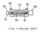
- FIG. 1 is a side view showing an example of the construction of a traveling wave tube
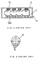
- FIG. 2 is schematic sectional view showing the structure of a collector in the traveling wave tube shown in FIG. 1 showing the relation between the high-voltage leads and the insulating ceramic parts.
- FIG. 3 is a sectional view showing the construction of an insulating ceramic part that is shown in FIG. 2.
- FIG. 2 shows a state in which high-voltage leads are routed through the lower-most portion of the insulating ceramic parts, but when four high-voltage leads pass through an insulating ceramic part as shown in FIG. 3, the high-voltage leads are not actually arranged at the lowermost portion but at positions that are slightly higher.
- the traveling wave tube is made up by: electron gun 50 having cathode 51 for emitting an electron beam; slow-wave circuit unit 60 made up by, for example, helix 61; magnetic focusing unit 70 made up by a periodic magnetic field generation device; input unit 80 for receiving the high-frequency signal that is the object of amplification; output unit 90 for outputting the high-frequency signal that has been amplified; and collector 100 of multistage collector structure.
- the electron beam that is emitted from cathode 51 advances inside helix 61 while interacting with the high-frequency signal that has been received from input unit 80.
- a high-frequency signal that has been amplified by interaction with the electron beam is then outputted from output unit 90.
- the electron beam has an energy distribution, is applied to collector 100, and is acquired at each collector electrode of collector 100.
- collector 100 of a traveling wave tube of the prior art is a structure in which a plurality of collector electrodes (four stages in FIG. 2) 11 are each bonded and secured by insulating ceramic parts 12 in the radial direction of vacuum envelope 13 that is composed of metal.
- High-voltage leads 14 are connected to each collector electrode 11 to supply prescribed voltages from the outside, and these high-voltage leads 14 are routed to the outside through holes that are provided in insulating ceramic parts 12.
- insulating ceramic parts 12 are of a construction formed in a cylindrical shape having uniform thickness in the radial direction so as to maintain a prescribed insulating capacity between vacuum envelope 13, which is connected to the ground potential, and collector electrodes 11, to which high voltages are applied; and in which a plurality of holes 15 are formed for routing the above-described high-voltage leads 14.
- the central axis of the inside diameter substantially coincides with the central axis of the outside diameter of these insulating ceramic parts 12.
- one high-voltage lead 14 passes through insulating ceramic part 12 that supports the first-stage collector electrode (C1 in FIG. 2), and two high-voltage leads 14 pass through insulating ceramic part 12 that supports the second-stage collector electrode (C2 in FIG. 2). Further, three high-voltage leads 14 pass through insulating ceramic part 12 that supports the third-stage collector electrode (C3 in FIG. 2), and four high-voltage leads 14 pass through insulating ceramic part 12 that supports the fourth-stage collector electrode (C4 in FIG. 2). In other words, high-voltage leads 14 do not pass through all of holes 15 provided in insulating ceramic parts 12. Nevertheless, the same number of holes are provided at the same positions such that the same insulating ceramic parts 12 can be used at any stage in collector 100 of the prior art.
- collector 100 shown in FIG. 2 is a construction having an exhaust pipe attached (not shown in the figure), this exhaust pipe normally being affixed in an upper location of FIG. 2, and holes 15 for high-voltage leads in insulating ceramic parts 12 are therefore all formed on the lower side, as shown in FIG. 3.
- the thickness of the insulating ceramic parts in the radial direction must be equal to or greater than a prescribed thickness depending on the dielectric strength of the insulating ceramic material in order to maintain an insulative property between each of the high-voltage leads and between the collector electrodes and the vacuum envelope.
- the insulating ceramic parts for insulating the collector electrodes and vacuum envelope in the traveling wave tube of the present invention are formed in a cylindrical shape in which the central axis of the inner diameter diverges from the central axis of the outer diameter.
- the traveling wave tube of the present invention is further constructed such that holes are provided in those portions having greater thickness in the radial direction, and the high-voltage leads for supplying prescribed voltages to the collector electrodes are routed through these holes.
- the diameter of the vacuum envelope can be made smaller than in the prior art while maintaining a prescribed insulative property between each of the high-voltage leads as well as between the collector electrodes and the vacuum envelope.
- FIG. 4 is a side sectional view showing the construction of the first embodiment of a collector in a traveling wave tube of the present invention
- FIG. 5 is a sectional view showing the construction of an insulating ceramic part shown in FIG. 4.
- the constitution of the traveling wave tube is similar to that of the prior art, and the explanation will therefore be abbreviated.
- the collector that is included in the traveling wave tube of the first embodiment is a construction in which, similar to the prior art, a plurality of collector electrodes (four stages in FIG. 4) 1 are bonded and secured by means of insulating ceramic parts 2 in the radial direction of vacuum envelope 3, which is composed of metal.
- the collector shown in FIG. 4 is structured such that the high-voltage lead that connects to the final-stage collector electrode (C4 in FIG. 4) is led directly to the exterior without passing through insulating ceramic part 2.
- the number of holes for routing high-voltage leads 4 that are provided in each insulating ceramic part 2 is therefore three.
- insulating ceramic part 2 of the present embodiment is a construction that is formed in a cylindrical shape in which the central axis of the inner diameter diverges from the central axis of the outer diameter, a plurality of holes 5 for routing high-voltage leads 4 being provided in the portion that is thicker in the radial direction.
- the thickness of insulating ceramic part 2 is formed such that a prescribed insulative property can be maintained between each of collector electrodes 1 and vacuum envelope 3 even at the point of least thickness of insulating ceramic parts 2 (point A in FIG. 5).
- holes 5 for routing high-voltage leads 4 are formed at positions such that, of the portions that are interposed between the outer circumference of holes 5 and vacuum envelope 3, the thickness at that portion having the least thickness (position B in FIG. 5) is a thickness that allows maintenance of an insulative property that is equivalent to the insulative property between above-described collector electrode 1 and vacuum envelope 3.
- holes 5 for routing high-voltage leads 4 are formed at positions at which the thickness of the portion of least thickness of the portions that are interposed between the outer circumference of holes 5 and vacuum envelope 3 is equal to or greater than the thickness of the point of least thickness of insulating ceramic part 2 in the radial direction.
- holes 5 are arranged at prescribed distances necessary for establishing an insulative property between high-voltage leads 4.
- a traveling wave tube that is more compact than the prior art can thus be obtained.
- using the traveling wave tube of the present embodiment in a system such as a phased-array antenna in which a multiplicity of antenna elements are arranged contributes greatly to a realizing more compact system.
- FIG. 6 is a schematic sectional view showing the construction of the second embodiment of the collector of a traveling wave tube of the present invention and showing the relation between the high-voltage leads and the insulating ceramic parts; and
- FIG. 7 is a sectional view showing the construction of an insulating ceramic part that is shown in FIG. 6.
- the collector shown in FIG. 6 is a construction having four stages of collector electrodes, this being a construction in which each high-voltage lead for applying voltage to each collector electrode passes through holes that are provided in the insulating ceramic parts and led to the outside.
- FIG. 6 shows a case in which high-voltage leads are routed through the region in which the insulating ceramic parts are thickest in the radial direction (the lowermost portion), but when four high-voltage leads pass through the insulating ceramic parts as in the present embodiment, the high-voltage leads actually pass through points that are slightly higher than the lowermost portion.
- the construction is equivalent to that of the first embodiment, and redundant explanation is therefore omitted.
- the collector of the present embodiment is constructed such that holes 6 that are provided in the insulating ceramic parts for the passage of the high-voltage leads differ according to the position of the collector electrodes.
- one hole 6 1 for the passage of the high-voltage lead is provided in the insulating ceramic part that supports the first-stage collector electrode (C1 in FIG. 6), and two holes 6 1 and 6 2 are provided in the insulating ceramic part that supports the second-stage collector electrode (C2 in FIG. 6).
- holes 6 1 -6 3 are provided in the insulating ceramic part that supports the third-stage collector electrode (C3 in FIG. 6), and four holes 6 1 -6 4 are provided in the insulating ceramic part that supports the last-stage collector electrode (C4 in FIG. 6).
Landscapes
- Engineering & Computer Science (AREA)
- Power Engineering (AREA)
- Microwave Tubes (AREA)
Applications Claiming Priority (2)
| Application Number | Priority Date | Filing Date | Title |
|---|---|---|---|
| JP2001381260A JP3577032B2 (ja) | 2001-12-14 | 2001-12-14 | 進行波管 |
| JP2001381260 | 2001-12-14 |
Publications (3)
| Publication Number | Publication Date |
|---|---|
| EP1322035A2 true EP1322035A2 (de) | 2003-06-25 |
| EP1322035A3 EP1322035A3 (de) | 2004-08-11 |
| EP1322035B1 EP1322035B1 (de) | 2008-03-05 |
Family
ID=19187310
Family Applications (1)
| Application Number | Title | Priority Date | Filing Date |
|---|---|---|---|
| EP02027622A Expired - Lifetime EP1322035B1 (de) | 2001-12-14 | 2002-12-11 | Wanderfeldröhre |
Country Status (4)
| Country | Link |
|---|---|
| US (1) | US6727651B2 (de) |
| EP (1) | EP1322035B1 (de) |
| JP (1) | JP3577032B2 (de) |
| DE (1) | DE60225412T2 (de) |
Cited By (1)
| Publication number | Priority date | Publication date | Assignee | Title |
|---|---|---|---|---|
| WO2003077273A3 (en) * | 2002-03-05 | 2004-12-29 | L 3 Comm Corp | High power density collector |
Families Citing this family (3)
| Publication number | Priority date | Publication date | Assignee | Title |
|---|---|---|---|---|
| US8935286B1 (en) * | 2011-06-16 | 2015-01-13 | The Boeing Company | Interactive system for managing parts and information for parts |
| DE102012100132A1 (de) | 2012-01-10 | 2013-07-11 | Thales Air Systems & Electron Devices Gmbh | Auffänger für eine Wanderfeldröhre und Wanderfeldröhre mit einem solchen Auffänger |
| CN110620028B (zh) * | 2019-09-27 | 2021-11-16 | 南京三乐集团有限公司 | 小型化、轻重量的Ka波段空间行波管 |
Family Cites Families (7)
| Publication number | Priority date | Publication date | Assignee | Title |
|---|---|---|---|---|
| JPS5888762A (ja) | 1981-11-24 | 1983-05-26 | Canon Inc | 電子写真用トナ− |
| DE3438520A1 (de) * | 1984-10-20 | 1986-04-24 | Licentia Patent-Verwaltungs-Gmbh, 6000 Frankfurt | Elektronenauffaenger fuer lauffeldroehre und lauffeldroehre mit einem solchen elektronenauffaenger |
| US4794303A (en) * | 1987-01-22 | 1988-12-27 | Litton Systems, Inc. | Axisymmetric electron collector with off-axis beam injection |
| JP3038830B2 (ja) * | 1990-07-26 | 2000-05-08 | 日本電気株式会社 | 伝導冷却形多段コレクタ |
| JPH04359839A (ja) * | 1991-06-06 | 1992-12-14 | Nec Corp | マイクロ波管 |
| JP3147838B2 (ja) * | 1997-11-14 | 2001-03-19 | 日本電気株式会社 | 進行波管のコレクタ構造 |
| JP3334694B2 (ja) * | 1999-10-19 | 2002-10-15 | 日本電気株式会社 | 進行波管 |
-
2001
- 2001-12-14 JP JP2001381260A patent/JP3577032B2/ja not_active Expired - Lifetime
-
2002
- 2002-12-11 EP EP02027622A patent/EP1322035B1/de not_active Expired - Lifetime
- 2002-12-11 DE DE60225412T patent/DE60225412T2/de not_active Expired - Lifetime
- 2002-12-12 US US10/317,096 patent/US6727651B2/en not_active Expired - Lifetime
Cited By (1)
| Publication number | Priority date | Publication date | Assignee | Title |
|---|---|---|---|---|
| WO2003077273A3 (en) * | 2002-03-05 | 2004-12-29 | L 3 Comm Corp | High power density collector |
Also Published As
| Publication number | Publication date |
|---|---|
| US20030117076A1 (en) | 2003-06-26 |
| US6727651B2 (en) | 2004-04-27 |
| JP3577032B2 (ja) | 2004-10-13 |
| EP1322035B1 (de) | 2008-03-05 |
| EP1322035A3 (de) | 2004-08-11 |
| JP2003187715A (ja) | 2003-07-04 |
| DE60225412D1 (de) | 2008-04-17 |
| DE60225412T2 (de) | 2009-02-26 |
Similar Documents
| Publication | Publication Date | Title |
|---|---|---|
| US10681794B1 (en) | Tri-axis x-ray tube | |
| US5120949A (en) | Semiconductor anode photomultiplier tube | |
| US6747412B2 (en) | Traveling wave tube and method of manufacture | |
| US6727651B2 (en) | Traveling wave tube | |
| US5272411A (en) | Coaxial triode apparatus | |
| US6147447A (en) | Electronic gun for multibeam electron tube and multibeam electron tube with the electron gun | |
| RU2084042C1 (ru) | Клистрод | |
| EP0203805A2 (de) | Elektronenkanone | |
| EP0589606A2 (de) | Elektronenstrahlerzeugungsvorrichtungen | |
| US3662212A (en) | Depressed electron beam collector | |
| US6670760B2 (en) | Collector structure of traveling wave tube having a lossy ceramic member | |
| JPH02183939A (ja) | マイクロ波管の真空気密窓及びこの窓を備える進行波管 | |
| EP0696048B1 (de) | Elektronenstrahlröhre | |
| US6407495B1 (en) | Electron beam tube having particular structure of the vacuum envelope containing electron gun | |
| US20260100322A1 (en) | Collector for a traveling wave tube and traveling wave tube with such a collector | |
| EP1565926B1 (de) | Elektronenröhre mit mehrstufigem Bremsfeldkollektor | |
| JP3334694B2 (ja) | 進行波管 | |
| US6462324B1 (en) | Photomultiplier tube with an improved dynode aperture mesh design | |
| JP2677212B2 (ja) | 直線ビームマイクロ波管の製造方法 | |
| RU2344513C2 (ru) | Модульная рентгеновская трубка, а также способ изготовления такой модульной рентгеновской трубки | |
| EP1568056B1 (de) | Elektronenstrahlröhre | |
| GB2271020A (en) | Electron gun arrangements | |
| Ghosh et al. | Development of a high efficiency travelling-wave tube for satellite communication | |
| Vancil | Traveling wave tube and method of manufacture | |
| JP2001210244A (ja) | 多極電子管 |
Legal Events
| Date | Code | Title | Description |
|---|---|---|---|
| PUAI | Public reference made under article 153(3) epc to a published international application that has entered the european phase |
Free format text: ORIGINAL CODE: 0009012 |
|
| AK | Designated contracting states |
Designated state(s): AT BE BG CH CY CZ DE DK EE ES FI FR GB GR IE IT LI LU MC NL PT SE SI SK TR |
|
| AX | Request for extension of the european patent |
Extension state: AL LT LV MK RO |
|
| PUAL | Search report despatched |
Free format text: ORIGINAL CODE: 0009013 |
|
| AK | Designated contracting states |
Kind code of ref document: A3 Designated state(s): AT BE BG CH CY CZ DE DK EE ES FI FR GB GR IE IT LI LU MC NL PT SE SI SK TR |
|
| AX | Request for extension of the european patent |
Extension state: AL LT LV MK RO |
|
| 17P | Request for examination filed |
Effective date: 20040706 |
|
| AKX | Designation fees paid |
Designated state(s): DE FR |
|
| RBV | Designated contracting states (corrected) |
Designated state(s): DE FR |
|
| GRAP | Despatch of communication of intention to grant a patent |
Free format text: ORIGINAL CODE: EPIDOSNIGR1 |
|
| GRAS | Grant fee paid |
Free format text: ORIGINAL CODE: EPIDOSNIGR3 |
|
| GRAA | (expected) grant |
Free format text: ORIGINAL CODE: 0009210 |
|
| AK | Designated contracting states |
Kind code of ref document: B1 Designated state(s): DE FR |
|
| REF | Corresponds to: |
Ref document number: 60225412 Country of ref document: DE Date of ref document: 20080417 Kind code of ref document: P |
|
| ET | Fr: translation filed | ||
| PLBE | No opposition filed within time limit |
Free format text: ORIGINAL CODE: 0009261 |
|
| STAA | Information on the status of an ep patent application or granted ep patent |
Free format text: STATUS: NO OPPOSITION FILED WITHIN TIME LIMIT |
|
| 26N | No opposition filed |
Effective date: 20081208 |
|
| REG | Reference to a national code |
Ref country code: FR Ref legal event code: TQ |
|
| REG | Reference to a national code |
Ref country code: DE Ref legal event code: R082 Ref document number: 60225412 Country of ref document: DE Representative=s name: VOSSIUS & PARTNER PATENTANWAELTE RECHTSANWAELT, DE Ref country code: DE Ref legal event code: R081 Ref document number: 60225412 Country of ref document: DE Owner name: NEC NETWORK AND SENSOR SYSTEMS, LTD., FUCHU-SH, JP Free format text: FORMER OWNER: NETCOMSEC CO. LTD., NIPPON HOSO KYOKAI, , JP Ref country code: DE Ref legal event code: R081 Ref document number: 60225412 Country of ref document: DE Owner name: NIPPON HOSO KYOKAI, JP Free format text: FORMER OWNER: NETCOMSEC CO. LTD., NIPPON HOSO KYOKAI, , JP Ref country code: DE Ref legal event code: R081 Ref document number: 60225412 Country of ref document: DE Owner name: NIPPON HOSO KYOKAI, JP Free format text: FORMER OWNERS: NETCOMSEC CO. LTD., FUCHU-SHI, TOKYO, JP; NIPPON HOSO KYOKAI, TOKIO/TOKYO, JP Ref country code: DE Ref legal event code: R081 Ref document number: 60225412 Country of ref document: DE Owner name: NEC NETWORK AND SENSOR SYSTEMS, LTD., FUCHU-SH, JP Free format text: FORMER OWNERS: NETCOMSEC CO. LTD., FUCHU-SHI, TOKYO, JP; NIPPON HOSO KYOKAI, TOKIO/TOKYO, JP |
|
| REG | Reference to a national code |
Ref country code: FR Ref legal event code: TQ Owner name: NEC NETWORK AND SENSOR SYSTEMS, LTD., JP Effective date: 20150908 Ref country code: FR Ref legal event code: TQ Owner name: NIPPON HOSO KYOKAI, JP Effective date: 20150908 |
|
| REG | Reference to a national code |
Ref country code: FR Ref legal event code: PLFP Year of fee payment: 14 |
|
| REG | Reference to a national code |
Ref country code: FR Ref legal event code: PLFP Year of fee payment: 15 |
|
| REG | Reference to a national code |
Ref country code: FR Ref legal event code: PLFP Year of fee payment: 16 |
|
| PGFP | Annual fee paid to national office [announced via postgrant information from national office to epo] |
Ref country code: DE Payment date: 20211210 Year of fee payment: 20 Ref country code: FR Payment date: 20211224 Year of fee payment: 20 |
|
| REG | Reference to a national code |
Ref country code: DE Ref legal event code: R071 Ref document number: 60225412 Country of ref document: DE |