US6670760B2 - Collector structure of traveling wave tube having a lossy ceramic member - Google Patents

Collector structure of traveling wave tube having a lossy ceramic member Download PDF

Info

Publication number
US6670760B2
US6670760B2 US09/849,527 US84952701A US6670760B2 US 6670760 B2 US6670760 B2 US 6670760B2 US 84952701 A US84952701 A US 84952701A US 6670760 B2 US6670760 B2 US 6670760B2
Authority
US
United States
Prior art keywords
collector
collector electrode
loss
traveling wave
outer enclosure
Prior art date
Legal status (The legal status is an assumption and is not a legal conclusion. Google has not performed a legal analysis and makes no representation as to the accuracy of the status listed.)
Expired - Fee Related, expires
Application number
US09/849,527
Other versions
US20010017521A1 (en
Inventor
Wako Suzuki
Takeshi Nobe
Current Assignee (The listed assignees may be inaccurate. Google has not performed a legal analysis and makes no representation or warranty as to the accuracy of the list.)
Netcomsec Co Ltd
Original Assignee
NEC Microwave Tube Ltd
Priority date (The priority date is an assumption and is not a legal conclusion. Google has not performed a legal analysis and makes no representation as to the accuracy of the date listed.)
Filing date
Publication date
Application filed by NEC Microwave Tube Ltd filed Critical NEC Microwave Tube Ltd
Priority to US09/849,527 priority Critical patent/US6670760B2/en
Publication of US20010017521A1 publication Critical patent/US20010017521A1/en
Assigned to NEC MICROWAVE TUBE, LTD. reassignment NEC MICROWAVE TUBE, LTD. ASSIGNMENT OF ASSIGNORS INTEREST (SEE DOCUMENT FOR DETAILS). Assignors: NEC CORPORATION
Application granted granted Critical
Publication of US6670760B2 publication Critical patent/US6670760B2/en
Assigned to NETCOMSEC CO. LTD reassignment NETCOMSEC CO. LTD ASSIGNMENT OF ASSIGNORS INTEREST (SEE DOCUMENT FOR DETAILS). Assignors: NEC MICROWAVE TUBE, LTD.
Adjusted expiration legal-status Critical
Expired - Fee Related legal-status Critical Current

Links

Images

Classifications

    • HELECTRICITY
    • H01ELECTRIC ELEMENTS
    • H01JELECTRIC DISCHARGE TUBES OR DISCHARGE LAMPS
    • H01J23/00Details of transit-time tubes of the types covered by group H01J25/00
    • H01J23/36Coupling devices having distributed capacitance and inductance, structurally associated with the tube, for introducing or removing wave energy
    • H01J23/54Filtering devices preventing unwanted frequencies or modes to be coupled to, or out of, the interaction circuit; Prevention of high frequency leakage in the environment
    • HELECTRICITY
    • H01ELECTRIC ELEMENTS
    • H01JELECTRIC DISCHARGE TUBES OR DISCHARGE LAMPS
    • H01J23/00Details of transit-time tubes of the types covered by group H01J25/00
    • H01J23/02Electrodes; Magnetic control means; Screens
    • H01J23/027Collectors

Definitions

  • This invention relates to a collector of a traveling wave tube.
  • FIGS. 4, 5 ( a ), 5 ( b ) and 6 are longitudinal cross-sectional views of a conventional traveling wave tube. Specifically, FIG. 4 shows a conduction cooling type, FIG. 5 a forced air-cooling type and FIG. 6 shows a water-cooling type.
  • FIG. 7 shows a longitudinal cross-sectional view of a conventional collector
  • FIG. 8 a is a transverse cross-sectional view of another illustrative structure of a conventional collector
  • FIG. 8 b is a longitudinal cross-sectional view of FIG. 8 a
  • FIG. 9 shows a two-stage version of the collector shown in FIG. 8 .
  • FIGS. 9 a and 9 b are a transverse cross-sectional view and a longitudinal cross-sectional view of the collector, respectively.
  • a traveling wave tube used as a relay station for micro-waves and for satellite communication.
  • a traveling wave tube includes an electron gun 23 for radiating an electron beam 24 , a delay wave circuit 25 for producing interaction between the electron beam 24 and the input micro-wave, a collector 26 for collecting the electron beam 24 and a beam converging device 27 for converging the electron beam 24 .
  • a method known as a collector potential lowering method For increasing the efficiency of the traveling wave tube, a method known as a collector potential lowering method is used. This method consists in progressively lowering the potential applied across the collector electrode 28 (see FIG. 4) relative to the delay wave circuit 25 to lower the speed of the electron beam 24 colliding against the collector to decrease the energy generated in the collector electrode 28 . To this end, there is provided a collector-insulating ceramic element 36 for maintaining insulation between the collector 26 and the delay wave circuit 25 against high voltage.
  • the electron beam 24 emitted by the electron gun 23 traverses the delay wave circuit 25 to amplify a signal and is collected by the collector 26 .
  • the electron beam 24 captured by the collector 26 has its kinetic energy converted into thermal energy to raise the temperature of a collector electrode 28 (see FIG. 4 ).
  • the heat generated in the collector electrode 28 needs to be externally released.
  • a conduction cooling type collector 31 for releasing the heat from a base plate 30 to a heat sink 29 as shown in FIG. 4
  • a forced air-cooling type collector 33 by providing a fin 32 on the outer periphery of the collector for flowing air thereon to release the heat with assistance from base plate 30 as shown in FIG. 5
  • a water-cooling type collector 35 by providing a water-cooled pipe 34 passed through by water to release the collector heat with assistance from base plate 30 , as shown in FIG. 6 .
  • the collector structure of a conventional traveling wave tube includes an insulating enclosure 37 of ceramics etc. for insulating the collector electrode 28 , formed of copper, molybdenum or graphite etc., for maintaining vacuum and air-tightness, a base plate 30 for supporting the collector electrode 28 and passing heat generated in the collector electrode 28 through the insulating member to release heat to the outside and a collector-insulating ceramic element 36 for maintaining insulation against the delay wave circuit.
  • These component parts are usually connected together by brazing or welding etc.
  • This structure is termed an external insulation type collector 38 .
  • JP Patent Kokai JP-A-2-101454 (1990) there is shown a structure in which the collector electrode 28 is supported by plural heat-conductive columnar ceramic elements 40 arranged between the collector electrode 28 and the external enclosure 41 to improve vibration-resistance and resistance against impact, while maintaining voltage withstand characteristics, as shown in FIGS. 8 a and 8 b .
  • This structure is termed an internal insulation type collector 39 .
  • the outer enclosure 41 , collector electrode 28 and the highly heat-conductive columnar ceramic elements 40 are secured in position by deforming the outer enclosure 41 such as by press-working. If, in this structure, plural collector electrodes 28 , specifically a first collector electrode 42 and a second collector electrode 43 , are used and arranged in this order from the upstream to the downstream side of the electron beam, it is possible to lower the potential of the second collector electrode 43 relative to the first collector electrode 42 to improve the overall efficiency of the traveling wave tube.
  • a two-stage collector 44 is illustrated in FIGS. 9 ( a ) and 9 ( b ).
  • An electron beam emitted by the electron gun is passed through the delay wave circuit to amplify the signal and is captured by the first collector electrode 42 and the second collector electrode 43 which are supported by heat-conductive columnar ceramic elements 40 .
  • a method of lowering the potential of the first collector electrode 42 to approximately 50% of that of the delay wave circuit and of lowering the potential of the second collector electrode 43 to approximately one-half that of the first collector electrode 42 This method consists in sequentially lowering the collector potential with respect to the potential of the delay wave circuit to lower the speed of the electron beam impinging against the collector in order to lower the energy produced in each collector electrode while improving the overall efficiency of the traveling wave tube.
  • the collector lead wire 45 of the first collector electrode 42 is taken out to a position forwardly or rearwardly of the outer enclosure 41 .
  • the collector lead wire is taken out to a position rearward of the outer enclosure 41 and is passed through the inside of an insulator tube 46 for maintaining insulation of the first collector lead wire 45 to reduce the size of the collector as shown in FIG. 9 ( b ).
  • This insulator tube 46 is led rearwardly of the collector via a groove 47 (see FIG. 9 ( a )) formed in a portion of the outer periphery of the second collector electrode 43 so as to be led to outside vacuum in an insulated state from a second collector lead line 48 (see FIG. 9 ( b )).
  • the electrical field is unavoidably concentrated in an edge portion of the insulator tube 46 . Since there is a corner portion of the groove 47 in this edge portion, a problem arises in that the withstand voltage is deteriorated between the first collector lead line and the ground potential.
  • the above-described collector structure of the conventional traveling wave tube is vulnerable to RF leakage from the collector lead line, such that, the RF power leakage occurs from the lead line portion if, in the case of the internal insulation type collector having a co-axial structure, impedance matching is taken between the collector lead line and the collector inlet end.
  • JP Patent Kokai JP-A-4-306538 (1992) there is disclosed a coupling cavity type traveling wave tube in which a loss member having loss in a high-impedance area and which is designed to suppress oscillations caused by the non-continuous coupling impedance in the high impedance area is arranged in the cavity.
  • the conventional technique of inserting this loss member is used in a high frequency circuit system (cavity 49 in FIG. 10) because the loss member 50 is of an electrically conductive material, as shown in the cross-sectional view of FIG. 10 .
  • the present invention provides a collector of an internal insulation type of a traveling wave tube having a structure in which a collector electrode is supported by a plurality of heat conductive columnar ceramic elements arranged between the collector electrode and an outer enclosure of the collector, wherein a loss ceramic member is arranged between the outer surface of the collector electrode and the inner surface of the outer enclosure of the collector.
  • the loss ceramic member is cylindrically-shaped (or annular) and contacted at outer corners thereof with the outer enclosure of the collector.
  • the loss ceramic member is contacted with the collector electrode at its inner corner diagonally opposite to the contacted portion thereof with the outer enclosure of the collector.
  • the loss ceramic member(s) is (are) those on the outer peripheral surface of which is coated with a conductive layer such as graphite coating.
  • a number corresponding to the number of the collector electrodes less 1 of the columnar ceramic elements is designed as cylindrically-shaped ceramic elements, if the number of the collector electrodes is two or more.
  • the cylindrically-shaped ceramic elements have a diameter equal to or less than the other heat conductive columnar ceramic elements.
  • the cylindrically-shaped ceramic elements are arranged in an area of the collector electrode from which heat is most unlikely to be released.
  • FIG. 1 a is a transverse cross-sectional view of a collector of a traveling wave tube according to the present invention taken along line II—II of FIG. 1 ( b ), and FIG. 1 b is a longitudinal cross-sectional view taken along line I—I of FIG. 1 a.
  • FIG. 2 shows transmission characteristics (S 21 ) of the collector of a traveling wave tube according to the present invention and transmission characteristics (S 21 ) in the absence of loss ceramic elements as a comparative embodiment.
  • FIG. 3 a is a transverse cross-sectional view of a second embodiment according to the present invention taken along line I—I of FIG. 3 ( b ), and FIG. 3 b is a longitudinal cross-sectional view taken along line II—II of FIG. 3 a.
  • FIG. 4 is a longitudinal cross-sectional view showing a structure of a conventional traveling wave tube of the conduction cooling type.
  • FIG. 5 ( a ) is a longitudinal cross-sectional view and FIG. 5 ( b ) is a transverse view of FIG. 5 ( a ) of a structure of a conventional traveling wave tube of the forced air cooling type.
  • FIG. 6 is a longitudinal cross-sectional view showing a structure of a conventional traveling wave tube of the water cooling type.
  • FIG. 7 is a longitudinal cross-sectional view showing an example of a conventional collector.
  • FIG. 8 a is a transverse cross-sectional view of another conventional collector taken along line I—I of FIG. 8 b
  • FIG. 8 b is a longitudinal cross-sectional view taken along line II—II of FIG. 8 a.
  • FIG. 9 a is a transverse cross-sectional view of a two-stage collector configuration and FIG. 9 b is a longitudinal cross-sectional view taken along line I—I of FIG. 9 ( a ).
  • FIG. 10 is a transverse cross-sectional view of a cavity employing a conventional loss ceramic element.
  • an internal insulating collector of the type in which a collector electrode ( 2 of FIGS. 1 ( a ) and 1 ( b )) is supported by plural heat conductive columnar ceramic elements ( 3 of FIGS. 1 ( a ) and 1 ( b )) arranged between the electrode and an outer enclosure ( 4 of FIGS. 1 ( a ) and 1 ( b )), in which loss ceramic members displaying significant loss (high frequency loss or dielectric loss) and superior insulating properties ( 5 of FIG.
  • the loss ceramic members are cylindrically-shaped (annular ring), the outer diametrical portion of each loss ceramic member contacts with the outer enclosure of the collector and the corner of the inner diametrical portion of the loss ceramic member disposed diametrically to the contacting portion contacts with the collector electrode. This realizes axial positioning of the collector while maintaining vibration-resistance and impact-resistance.
  • a number corresponding to the number of the collector electrodes less 1 of the columnar ceramic elements are designed as cylindrically-shaped (e.g., hollow) ceramic element(s), if the number of the collector electrodes is two or more.
  • the cylindrically-shaped ceramic element(s) has a diameter equal to or smaller than the other heat conductive columnar ceramic elements.
  • these cylindrically-shaped ceramic elements are disposed without any groove formed in the second collector (on the outer periphery thereof) for laying conventional insulating tubes as in the conventional collector.
  • the cylindrically-shaped ceramic element(s) is positioned in an area from which heat of the collector electrode is most unlikely to be released (or dissipated), for example, on the opposite side to the base plate in case of conduction cooling, towards the base plate in case of the forced air cooling, and in an area of lesser congestion of water-cooling pipes in case of forced water cooling.
  • the collector of the present embodiment of the present invention in which loss ceramic members superior in insulation properties are arranged forwardly and rearwardly of the collector for preventing RF leakage from the collector, and collector lead wire is passed through the inside of the cylindrically-shaped (hollow) heat conductive columnar ceramic elements designed for collector insulation, voltage withstand characteristics can be improved while vibration-resistance and impact-resistance equivalent to those in the conventional system are maintained, and also RF leakage may be prevented from occurring from the collector.
  • FIGS. 1 ( a ) and 1 ( b ) show a collector structure of a traveling wave tube (or guide) embodying the present invention.
  • FIG. 1 a is a transverse cross-sectional view of an internal insulating type collector of a traveling wave tube
  • FIG. 1 b is a longitudinal cross-sectional sectional view taken along line II—II of FIG. 1 a.
  • a collector 1 of a travelling wave tube of the present embodiment is made up of a collector electrode 2 , heat conductive columnar ceramic elements 3 , an outer enclosure 4 for maintaining vacuum and loss ceramic members 5 (see FIG. 1 ( b )) provided forwardly or rearwardly of the collector electrode 2 .
  • the heat conductive columnar ceramic elements 3 are axially arranged (distributed) over the entire area (circumference) of an annular gap defined between the outer peripheral surface of the cylindrically-shaped collector electrode 2 and the inner peripheral surface of the cylindrically-shaped outer enclosure 4 .
  • the heat conductive columnar ceramic elements 3 are kept in contact with the collector electrode 2 by an outer flange thereof so that the ceramic elements 3 are not deflected at their axial ends.
  • the inner peripheral surface of the outer enclosure 4 is spaced apart at the axial end portions from the heat conductive columnar ceramic element 3 by annular gaps 6 , each of several mm. As a matter of course, the broader this gap, the lesser is the degree of concentration of the electrical field and the higher are voltage withstand characteristics.
  • the columnar ceramic elements 3 and the rear loss ceramic member 5 are axially secured on a shoulder formed at the outer peripheral corner of the end plate of outer enclosure 4 leaving an axial clearance.
  • the forward loss ceramic member 5 is axially and radially secured by an inward flange formed within the outer enclosure 4 , while the diagonally opposite corner of the loss ceramic member 5 is axially secured by the outward flange at the forward end of the collector electrode 2 .
  • the rear loss ceramic member 5 is radially secured on a small annular rib or protrusions axially extending from the rear end of the collector electrode 2 .
  • the cylindrically-shaped (annular ring) loss ceramic members 5 are arranged at both ends of the heat conductive columnar ceramic elements 3 so that a portion of the inner surface 5 b (see FIG. 1 ( b )) of each member 5 (see FIG. 1 ( b )) is contacted with (secured by) the collector electrode 2 and the corner of the outer surface 5 a (see FIG. 1 ( b )) of the loss ceramic member lying diagonally opposite to the contacted portion with the collector electrode 2 is contacted with (secured by) the outer enclosure.
  • the loss ceramic members 5 are of alumina material etc. coated on outer sides with a graphite layer of Aquadag E (trade name of Nihon Atisson K. K., a mixture of graphite and an aqueous binder).
  • Aquadag E trade name of Nihon Atisson K. K., a mixture of graphite and an aqueous binder
  • the resulting assembly is pressed from outside such as press-working to take heat conduction into account to deform the outer enclosure 4 to secure the various components in situ.
  • FIG. 2 shows characteristics 8 as a transmission circuit (S 21 ) in the TEM mode of the collector 1 of the structure of the preset embodiment.
  • FIG. 2 shows, as a comparative embodiment, transmission characteristics 9 (S 21 ) in the absence of the loss ceramic members 5 .
  • RF signals were entered at an electron beam incident end of the collector 1 and the signal level thereof was measured from a collector terminal 11 (see FIG. 1 ( b )) connecting to a collector lead wire 10 (see FIG. 1 ( b )).
  • the signal level was improved by approximately 20 dB in the present embodiment.
  • the forward side loss ceramic member accounts for a loss of 10 dB
  • the rear side loss ceramic member accounts for a loss of 10 dB
  • FIGS. 3 ( a ) and 3 ( b ) show the collector structure 12 of the second embodiment of the present invention.
  • FIG. 3 a is a transverse cross-sectional view of the collector structure
  • FIG. 3 b is a longitudinal cross-sectional view taken along line II—II thereof.
  • the second embodiment of the present invention includes a first collector electrode 13 (see FIG. 3 ( b )), a second collector electrode 14 (see FIG. 3 ( b )), highly heat conductive columnar ceramic elements 15 (see FIG. 3 ( a )), an outer enclosure 16 for maintaining vacuum, loss ceramic members 17 (see FIG.
  • a first collector lead wire 18 (see FIG. 3 ( b )) extending from the first collector electrode 13 along the outer peripheral surface of the second collector electrode 14 to the rear side of the second collector via a cylindrically-shaped (hollow) ceramic element 19 for maintaining the insulation of the collector lead wire.
  • the first and second loss ceramic members 17 are axially secured between flanges formed on the collector electrodes 13 , 14 and outer enclosure 16 .
  • the forward loss ceramic member 17 is secured between an inward protruding flange of the outer enclosure 16 and the outward protruding flange at the forward end of the first collector electrode 13 .
  • the rearward loss ceramic member is secured between the inward protruding flange of the outer enclosure 16 and the outward flange at the rear end of the second collector electrode 14 .
  • the columnar ceramic elements are axially secured between two outward flanges of the first and second collector electrodes 13 , 14 .
  • the first collector lead wire 18 is lead to outside vacuum via a first collector terminal 20 (see FIG. 3 ( b )).
  • a second collector lead wire 21 (see FIG. 3 ( b )) is led to outside vacuum via a second collector terminal 22 (see FIG. 3 ( b )).
  • the first collector lead wire 18 is passed through the inside of cylindrically-shaped ceramic elements 19 , placed in lieu of the heat conductive columnar ceramic elements 15 , so as to be led to the rear side of the collector.
  • the outer diameter of the cylindrically-shaped ceramic elements 19 is equal to or less than the diameter of the heat conductive columnar ceramic elements.
  • the collector cooling method is of the conduction cooling type
  • the collector is placed on the opposite side of a portion of a base plate where the collector is contacted with a heat sink, that is on the side where heat dissipation is at the least level.
  • the collector cooling method is of the forced air cooling type or the water cooling type
  • the collector is placed on the side of the base plate carrying the collector where there is no air or water flow, that is towards the base plate carrying the collector. In short, the collector position is directly opposite to the conduction cooling position.
  • the present embodiment has an advantage that voltage withstand characteristics, vibration-resistance or impact-resistance and heat conductivity are equivalent to those of the first embodiment, even though the number of the collector stages is increased, thus assuring facilitated multi-stage collector designing.
  • Aquadag can be applied not only on the outer peripheral surfaces but also on the inner peripheral surfaces of the loss ceramic elements. Moreover, Aquadag can be applied to both surfaces of the loss ceramic elements if voltage withstand characteristics permit. Alternatively, Aquadag can be applied to a portion of the surfaces of the loss ceramic elements depending on the amount of RF leakage.
  • an internal insulation type collector in which, by placing loss ceramic elements on the collector, RF leakage from the collector may be prevented and axial position setting can also be achieved while vibration-resistance and impact-resistance equivalent to those of the conventional system are maintained, and yet the voltage withstand characteristics can be improved.
  • the present invention may be used in combination with other structures and elements of the conventional devices other than the specific features of the present invention.
  • the entire disclosure relating to the prior art is also incorporated by reference in the disclosure of the present invention.

Abstract

A collector of a traveling wave tube in which a larger quantity of loss ceramic members are arranged between an outer collector enclosure and an outer surface of a collector electrode for increasing high frequency loss to prevent RF leakage from the collector lead wire. The collector includes a collector electrode 2, heat conductive columnar ceramic elements 3, an outer collector enclosure 4 for maintaining vacuum and loss ceramic members 5 arranged between the outer surface of the collector electrode 2 and the inner surface of the outer collector enclosure 4.

Description

This is a Continuation Application of application Ser. No. 09/190,009 filed Nov. 12, 1998 (issued as U.S. Pat. No. 6,291,935 on Sep. 18, 2001), the disclosure of which is incorporated herein by reference.
FIELD OF THE INVENTION
This invention relates to a collector of a traveling wave tube.
BACKGROUND OF THE INVENTION
FIGS. 4, 5(a), 5(b) and 6 are longitudinal cross-sectional views of a conventional traveling wave tube. Specifically, FIG. 4 shows a conduction cooling type, FIG. 5 a forced air-cooling type and FIG. 6 shows a water-cooling type.
FIG. 7 shows a longitudinal cross-sectional view of a conventional collector, while FIG. 8a is a transverse cross-sectional view of another illustrative structure of a conventional collector and FIG. 8b is a longitudinal cross-sectional view of FIG. 8a. FIG. 9 shows a two-stage version of the collector shown in FIG. 8. Specifically, FIGS. 9a and 9 b are a transverse cross-sectional view and a longitudinal cross-sectional view of the collector, respectively.
Among the devices which effect amplification of the micro-wave, using an electron beam, there is a traveling wave tube used as a relay station for micro-waves and for satellite communication.
Referring to FIGS. 4, 5(a), 5(b) and 6, a traveling wave tube includes an electron gun 23 for radiating an electron beam 24, a delay wave circuit 25 for producing interaction between the electron beam 24 and the input micro-wave, a collector 26 for collecting the electron beam 24 and a beam converging device 27 for converging the electron beam 24.
For increasing the efficiency of the traveling wave tube, a method known as a collector potential lowering method is used. This method consists in progressively lowering the potential applied across the collector electrode 28 (see FIG. 4) relative to the delay wave circuit 25 to lower the speed of the electron beam 24 colliding against the collector to decrease the energy generated in the collector electrode 28. To this end, there is provided a collector-insulating ceramic element 36 for maintaining insulation between the collector 26 and the delay wave circuit 25 against high voltage.
The electron beam 24 emitted by the electron gun 23 traverses the delay wave circuit 25 to amplify a signal and is collected by the collector 26. At this time, the electron beam 24 captured by the collector 26 has its kinetic energy converted into thermal energy to raise the temperature of a collector electrode 28 (see FIG. 4).
For this reason, the heat generated in the collector electrode 28 (see FIG. 4) needs to be externally released. Among the methods for releasing the heat, there are a conduction cooling type collector 31 for releasing the heat from a base plate 30 to a heat sink 29, as shown in FIG. 4, a forced air-cooling type collector 33 by providing a fin 32 on the outer periphery of the collector for flowing air thereon to release the heat with assistance from base plate 30, as shown in FIG. 5, and a water-cooling type collector 35 by providing a water-cooled pipe 34 passed through by water to release the collector heat with assistance from base plate 30, as shown in FIG. 6.
Referring to FIG. 7, the collector structure of a conventional traveling wave tube includes an insulating enclosure 37 of ceramics etc. for insulating the collector electrode 28, formed of copper, molybdenum or graphite etc., for maintaining vacuum and air-tightness, a base plate 30 for supporting the collector electrode 28 and passing heat generated in the collector electrode 28 through the insulating member to release heat to the outside and a collector-insulating ceramic element 36 for maintaining insulation against the delay wave circuit. These component parts are usually connected together by brazing or welding etc. This structure is termed an external insulation type collector 38.
In the above-described collector, there are occasions where the collector electrode is displaced in the axial direction due to mechanical vibrations or impact. This positional deviation occasionally leads to changes in the colliding position of the electron beam leading to emission of gases or leading to an increased amount of retrogressive electrons to increase the helical current of the traveling wave tube, occasionally leading to destruction of the tube bulb.
Also, in such a collector structure, a problem arises in that RE components (TEM mode) of the electron beam incident on the collector are subjected to RE leakage through a collector lead line or collector-insulating ceramic element.
In JP Patent Kokai JP-A-2-101454 (1990), there is shown a structure in which the collector electrode 28 is supported by plural heat-conductive columnar ceramic elements 40 arranged between the collector electrode 28 and the external enclosure 41 to improve vibration-resistance and resistance against impact, while maintaining voltage withstand characteristics, as shown in FIGS. 8a and 8 b. This structure is termed an internal insulation type collector 39.
In this type of collector, the outer enclosure 41, collector electrode 28 and the highly heat-conductive columnar ceramic elements 40 are secured in position by deforming the outer enclosure 41 such as by press-working. If, in this structure, plural collector electrodes 28, specifically a first collector electrode 42 and a second collector electrode 43, are used and arranged in this order from the upstream to the downstream side of the electron beam, it is possible to lower the potential of the second collector electrode 43 relative to the first collector electrode 42 to improve the overall efficiency of the traveling wave tube.
A two-stage collector 44 is illustrated in FIGS. 9(a) and 9(b). An electron beam emitted by the electron gun is passed through the delay wave circuit to amplify the signal and is captured by the first collector electrode 42 and the second collector electrode 43 which are supported by heat-conductive columnar ceramic elements 40.
For improving the efficiency of the traveling wave tube, there is usually employed a method of lowering the potential of the first collector electrode 42 to approximately 50% of that of the delay wave circuit and of lowering the potential of the second collector electrode 43 to approximately one-half that of the first collector electrode 42. This method consists in sequentially lowering the collector potential with respect to the potential of the delay wave circuit to lower the speed of the electron beam impinging against the collector in order to lower the energy produced in each collector electrode while improving the overall efficiency of the traveling wave tube.
Referring to FIG. 9(b), in the case of a two-stage internal insulation type collector 44, it is necessary to take out a first collector lead wire 45 of the first collector electrode 42 to a position forwardly or rearwardly of the outer enclosure 41. In the present case, the collector lead wire is taken out to a position rearward of the outer enclosure 41 and is passed through the inside of an insulator tube 46 for maintaining insulation of the first collector lead wire 45 to reduce the size of the collector as shown in FIG. 9(b). This insulator tube 46 is led rearwardly of the collector via a groove 47 (see FIG. 9(a)) formed in a portion of the outer periphery of the second collector electrode 43 so as to be led to outside vacuum in an insulated state from a second collector lead line 48 (see FIG. 9(b)).
In this structure, the electrical field is unavoidably concentrated in an edge portion of the insulator tube 46. Since there is a corner portion of the groove 47 in this edge portion, a problem arises in that the withstand voltage is deteriorated between the first collector lead line and the ground potential.
In addition to this structure, a demand is raised in recent years for providing a small-sized lightweight structure easy to manufacture for communication or loading on a satellite to lower the cost.
SUMMARY OF THE INVENTION
The above-described collector structure of the conventional traveling wave tube is vulnerable to RF leakage from the collector lead line, such that, the RF power leakage occurs from the lead line portion if, in the case of the internal insulation type collector having a co-axial structure, impedance matching is taken between the collector lead line and the collector inlet end.
Meanwhile, in JP Patent Kokai JP-A-4-306538 (1992), for example, there is disclosed a coupling cavity type traveling wave tube in which a loss member having loss in a high-impedance area and which is designed to suppress oscillations caused by the non-continuous coupling impedance in the high impedance area is arranged in the cavity. The conventional technique of inserting this loss member is used in a high frequency circuit system (cavity 49 in FIG. 10) because the loss member 50 is of an electrically conductive material, as shown in the cross-sectional view of FIG. 10.
It is therefore an object of the present invention to provide a collector of a traveling wave tube capable of maintaining vibration-resistance, impact-resistance and voltage withstand characteristics and yet capable of suppressing or eliminating RF leakage.
For accomplishing the above object, the present invention provides a collector of an internal insulation type of a traveling wave tube having a structure in which a collector electrode is supported by a plurality of heat conductive columnar ceramic elements arranged between the collector electrode and an outer enclosure of the collector, wherein a loss ceramic member is arranged between the outer surface of the collector electrode and the inner surface of the outer enclosure of the collector.
Preferably, the loss ceramic member is cylindrically-shaped (or annular) and contacted at outer corners thereof with the outer enclosure of the collector. The loss ceramic member is contacted with the collector electrode at its inner corner diagonally opposite to the contacted portion thereof with the outer enclosure of the collector.
Preferably, the loss ceramic member(s) is (are) those on the outer peripheral surface of which is coated with a conductive layer such as graphite coating.
As for the plural heat conductive columnar ceramic elements, a number corresponding to the number of the collector electrodes less 1 of the columnar ceramic elements is designed as cylindrically-shaped ceramic elements, if the number of the collector electrodes is two or more. The cylindrically-shaped ceramic elements have a diameter equal to or less than the other heat conductive columnar ceramic elements. The cylindrically-shaped ceramic elements are arranged in an area of the collector electrode from which heat is most unlikely to be released.
Other features of the present invention are disclosed in the appended claims, the contents thereof being incorporated herein by reference thereto.
BRIEF DESCRIPTION OF THE DRAWINGS
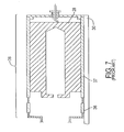
FIG. 1a is a transverse cross-sectional view of a collector of a traveling wave tube according to the present invention taken along line II—II of FIG. 1(b), and FIG. 1b is a longitudinal cross-sectional view taken along line I—I of FIG. 1a.
FIG. 2 shows transmission characteristics (S21) of the collector of a traveling wave tube according to the present invention and transmission characteristics (S21) in the absence of loss ceramic elements as a comparative embodiment.
FIG. 3a is a transverse cross-sectional view of a second embodiment according to the present invention taken along line I—I of FIG. 3(b), and FIG. 3b is a longitudinal cross-sectional view taken along line II—II of FIG. 3a.
FIG. 4 is a longitudinal cross-sectional view showing a structure of a conventional traveling wave tube of the conduction cooling type.
FIG. 5(a) is a longitudinal cross-sectional view and FIG. 5(b) is a transverse view of FIG. 5(a) of a structure of a conventional traveling wave tube of the forced air cooling type.
FIG. 6 is a longitudinal cross-sectional view showing a structure of a conventional traveling wave tube of the water cooling type.
FIG. 7 is a longitudinal cross-sectional view showing an example of a conventional collector.
FIG. 8a is a transverse cross-sectional view of another conventional collector taken along line I—I of FIG. 8b, and FIG. 8b is a longitudinal cross-sectional view taken along line II—II of FIG. 8a.
FIG. 9a is a transverse cross-sectional view of a two-stage collector configuration and FIG. 9b is a longitudinal cross-sectional view taken along line I—I of FIG. 9(a).
FIG. 10 is a transverse cross-sectional view of a cavity employing a conventional loss ceramic element.
PREFERRED EMBODIMENTS OF THE INVENTION
Preferred embodiments of the invention are explained further. In a preferred embodiment of the present invention, there is provided an internal insulating collector of the type in which a collector electrode (2 of FIGS. 1(a) and 1(b)) is supported by plural heat conductive columnar ceramic elements (3 of FIGS. 1(a) and 1(b)) arranged between the electrode and an outer enclosure (4 of FIGS. 1(a) and 1(b)), in which loss ceramic members displaying significant loss (high frequency loss or dielectric loss) and superior insulating properties (5 of FIG. 1(b)) are arranged between the outer surface of the collector electrode (surface not illuminated with an electron beam) and the inner surface of the outer enclosure of the collector (surface contacting with insulating ceramics). These loss ceramic members may be coated on their outer peripheral surface with a substance such as Aquadag (7 of FIG. 1(b)).
Preferably, according to a preferred embodiment of the present invention, the loss ceramic members are cylindrically-shaped (annular ring), the outer diametrical portion of each loss ceramic member contacts with the outer enclosure of the collector and the corner of the inner diametrical portion of the loss ceramic member disposed diametrically to the contacting portion contacts with the collector electrode. This realizes axial positioning of the collector while maintaining vibration-resistance and impact-resistance.
Among the plural heat conductive columnar ceramic elements, a number corresponding to the number of the collector electrodes less 1 of the columnar ceramic elements are designed as cylindrically-shaped (e.g., hollow) ceramic element(s), if the number of the collector electrodes is two or more. The cylindrically-shaped ceramic element(s) has a diameter equal to or smaller than the other heat conductive columnar ceramic elements. For improving voltage withstand characteristics, these cylindrically-shaped ceramic elements are disposed without any groove formed in the second collector (on the outer periphery thereof) for laying conventional insulating tubes as in the conventional collector. Meanwhile, the cylindrically-shaped ceramic element(s) is positioned in an area from which heat of the collector electrode is most unlikely to be released (or dissipated), for example, on the opposite side to the base plate in case of conduction cooling, towards the base plate in case of the forced air cooling, and in an area of lesser congestion of water-cooling pipes in case of forced water cooling.
With the collector of the present embodiment of the present invention, in which loss ceramic members superior in insulation properties are arranged forwardly and rearwardly of the collector for preventing RF leakage from the collector, and collector lead wire is passed through the inside of the cylindrically-shaped (hollow) heat conductive columnar ceramic elements designed for collector insulation, voltage withstand characteristics can be improved while vibration-resistance and impact-resistance equivalent to those in the conventional system are maintained, and also RF leakage may be prevented from occurring from the collector.
Embodiments
Referring to the drawings, preferred embodiments of the present invention will be explained in detail.
[First Embodiment]
FIGS. 1(a) and 1(b) show a collector structure of a traveling wave tube (or guide) embodying the present invention. Specifically, FIG. 1 a is a transverse cross-sectional view of an internal insulating type collector of a traveling wave tube and FIG. 1b is a longitudinal cross-sectional sectional view taken along line II—II of FIG. 1a.
Referring to FIGS. 1(a) and 1(b), a collector 1 of a travelling wave tube of the present embodiment is made up of a collector electrode 2, heat conductive columnar ceramic elements 3, an outer enclosure 4 for maintaining vacuum and loss ceramic members 5 (see FIG. 1(b)) provided forwardly or rearwardly of the collector electrode 2.
The heat conductive columnar ceramic elements 3 are axially arranged (distributed) over the entire area (circumference) of an annular gap defined between the outer peripheral surface of the cylindrically-shaped collector electrode 2 and the inner peripheral surface of the cylindrically-shaped outer enclosure 4. The heat conductive columnar ceramic elements 3 are kept in contact with the collector electrode 2 by an outer flange thereof so that the ceramic elements 3 are not deflected at their axial ends. For improving voltage withstand characteristics, the inner peripheral surface of the outer enclosure 4 is spaced apart at the axial end portions from the heat conductive columnar ceramic element 3 by annular gaps 6, each of several mm. As a matter of course, the broader this gap, the lesser is the degree of concentration of the electrical field and the higher are voltage withstand characteristics.
Also, there is a small axial clearance between the columnar ceramic elements 3 and the rear loss ceramic member 5, which in turn is axially secured on a shoulder formed at the outer peripheral corner of the end plate of outer enclosure 4 leaving an axial clearance. The forward loss ceramic member 5 is axially and radially secured by an inward flange formed within the outer enclosure 4, while the diagonally opposite corner of the loss ceramic member 5 is axially secured by the outward flange at the forward end of the collector electrode 2. The rear loss ceramic member 5 is radially secured on a small annular rib or protrusions axially extending from the rear end of the collector electrode 2.
The cylindrically-shaped (annular ring) loss ceramic members 5 (see FIG. 1(b)) are arranged at both ends of the heat conductive columnar ceramic elements 3 so that a portion of the inner surface 5 b (see FIG. 1(b)) of each member 5 (see FIG. 1(b)) is contacted with (secured by) the collector electrode 2 and the corner of the outer surface 5 a (see FIG. 1(b)) of the loss ceramic member lying diagonally opposite to the contacted portion with the collector electrode 2 is contacted with (secured by) the outer enclosure.
The loss ceramic members 5 are of alumina material etc. coated on outer sides with a graphite layer of Aquadag E (trade name of Nihon Atisson K. K., a mixture of graphite and an aqueous binder).
After assembling the above structure of the entire collector, the resulting assembly is pressed from outside such as press-working to take heat conduction into account to deform the outer enclosure 4 to secure the various components in situ.
FIG. 2 shows characteristics 8 as a transmission circuit (S21) in the TEM mode of the collector 1 of the structure of the preset embodiment. FIG. 2 shows, as a comparative embodiment, transmission characteristics 9 (S21) in the absence of the loss ceramic members 5.
As a measurement method, RF signals were entered at an electron beam incident end of the collector 1 and the signal level thereof was measured from a collector terminal 11 (see FIG. 1(b)) connecting to a collector lead wire 10 (see FIG. 1(b)). As may be seen from FIG. 2, the signal level was improved by approximately 20 dB in the present embodiment.
It may be surmised that the forward side loss ceramic member accounts for a loss of 10 dB, while the rear side loss ceramic member accounts for a loss of 10 dB, thus achieving improvement of 20 dB.
[Second Embodiment]
As a second embodiment, an internal insulation type two-staged collector is explained.
FIGS. 3(a) and 3(b) show the collector structure 12 of the second embodiment of the present invention. Specifically, FIG. 3a is a transverse cross-sectional view of the collector structure and FIG. 3b is a longitudinal cross-sectional view taken along line II—II thereof. Referring to FIGS. 3(a) and 3(b), the second embodiment of the present invention includes a first collector electrode 13 (see FIG. 3(b)), a second collector electrode 14 (see FIG. 3(b)), highly heat conductive columnar ceramic elements 15 (see FIG. 3(a)), an outer enclosure 16 for maintaining vacuum, loss ceramic members 17 (see FIG. 3(b)), arranged forwardly of the first collector electrode 13 and rearwardly of the second collector electrode 14, a first collector lead wire 18 (see FIG. 3(b)) extending from the first collector electrode 13 along the outer peripheral surface of the second collector electrode 14 to the rear side of the second collector via a cylindrically-shaped (hollow) ceramic element 19 for maintaining the insulation of the collector lead wire.
The first and second loss ceramic members 17 are axially secured between flanges formed on the collector electrodes 13, 14 and outer enclosure 16. Namely, the forward loss ceramic member 17 is secured between an inward protruding flange of the outer enclosure 16 and the outward protruding flange at the forward end of the first collector electrode 13. The rearward loss ceramic member is secured between the inward protruding flange of the outer enclosure 16 and the outward flange at the rear end of the second collector electrode 14. The columnar ceramic elements are axially secured between two outward flanges of the first and second collector electrodes 13, 14.
The first collector lead wire 18 is lead to outside vacuum via a first collector terminal 20 (see FIG. 3(b)). In addition, a second collector lead wire 21 (see FIG. 3(b)) is led to outside vacuum via a second collector terminal 22 (see FIG. 3(b)).
The first collector lead wire 18 is passed through the inside of cylindrically-shaped ceramic elements 19, placed in lieu of the heat conductive columnar ceramic elements 15, so as to be led to the rear side of the collector. The outer diameter of the cylindrically-shaped ceramic elements 19 is equal to or less than the diameter of the heat conductive columnar ceramic elements.
If the collector cooling method is of the conduction cooling type, the collector is placed on the opposite side of a portion of a base plate where the collector is contacted with a heat sink, that is on the side where heat dissipation is at the least level. If the collector cooling method is of the forced air cooling type or the water cooling type, the collector is placed on the side of the base plate carrying the collector where there is no air or water flow, that is towards the base plate carrying the collector. In short, the collector position is directly opposite to the conduction cooling position.
The present embodiment has an advantage that voltage withstand characteristics, vibration-resistance or impact-resistance and heat conductivity are equivalent to those of the first embodiment, even though the number of the collector stages is increased, thus assuring facilitated multi-stage collector designing.
It is noted that the Aquadag can be applied not only on the outer peripheral surfaces but also on the inner peripheral surfaces of the loss ceramic elements. Moreover, Aquadag can be applied to both surfaces of the loss ceramic elements if voltage withstand characteristics permit. Alternatively, Aquadag can be applied to a portion of the surfaces of the loss ceramic elements depending on the amount of RF leakage.
The meritorious effects of the present invention are summarized as follows.
According to the present invention, as described above, there may be provided an internal insulation type collector in which, by placing loss ceramic elements on the collector, RF leakage from the collector may be prevented and axial position setting can also be achieved while vibration-resistance and impact-resistance equivalent to those of the conventional system are maintained, and yet the voltage withstand characteristics can be improved.
Moreover, according to the present invention, high heat conductivity and voltage withstand characteristics can be maintained in achieving multi-stage collecting designing in consideration of arrangement of the collector lead wires.
The present invention may be used in combination with other structures and elements of the conventional devices other than the specific features of the present invention. Thus the entire disclosure relating to the prior art is also incorporated by reference in the disclosure of the present invention.
Further any arbitrary combination of the disclosed features and/or elements may be done within the gist of the present invention irrespective of the place of disclosure including the entire claims.
It should be noted that other objects of the present invention will become apparent in the entire disclosure and that modifications may be done without departing the gist and scope of the present invention as disclosed herein and appended herewith.

Claims (2)

What is claimed is:
1. An internal insulation collector for a traveling wave tube having a structure in which a collector electrode is supported by a plurality of heat conductive columnar ceramic elements arranged between the collector electrode and an outer enclosure of the collector, and an inside of said collector electrode is arranged within an interior vacuum, wherein a loss ceramic member is arranged within said interior vacuum, said loss ceramic member being arranged between an outer surface of the collector electrode and an inner surface of the outer enclosure of the collector; and
wherein a conductive loss layer is disposed in direct contact with, and covering, at least a portion of a surface of the loss ceramic member.
2. An internal insulation collector for a traveling wave tube having a structure in which a collector electrode is supported by a plurality of heat conductive columnar ceramic elements arranged between the collector electrode and an outer enclosure of the collector, said outer enclosure of the collector having an inner peripheral surface with annular gaps at axial end portions of said heat conductive columnar ceramic elements, wherein
a portion of said collector electrode is illuminated with an electron beam;
an inside of said collector electrode is arranged within an interior vacuum; and
insulating loss ceramic members, displaying high frequency loss, are arranged within said interior vacuum, said insulating loss ceramic members being arranged between an outer surface of said collector electrode not illuminated with the electron beam and a surface of said outer enclosure in contact with said columnar ceramic elements; and
wherein at least one of said annular gaps between at least one axial end portion of the columnar ceramic elements and the outer enclosure improves voltage withstanding characteristics.
US09/849,527 1997-11-14 2001-05-07 Collector structure of traveling wave tube having a lossy ceramic member Expired - Fee Related US6670760B2 (en)

Priority Applications (1)

Application Number Priority Date Filing Date Title
US09/849,527 US6670760B2 (en) 1997-11-14 2001-05-07 Collector structure of traveling wave tube having a lossy ceramic member

Applications Claiming Priority (4)

Application Number Priority Date Filing Date Title
JP33119797A JP3147838B2 (en) 1997-11-14 1997-11-14 Traveling wave tube collector structure
JP9-331197 1997-11-14
US09/190,009 US6291935B1 (en) 1997-11-14 1998-11-12 Collector structure having a loss ceramic member
US09/849,527 US6670760B2 (en) 1997-11-14 2001-05-07 Collector structure of traveling wave tube having a lossy ceramic member

Related Parent Applications (1)

Application Number Title Priority Date Filing Date
US09/190,009 Continuation US6291935B1 (en) 1997-11-14 1998-11-12 Collector structure having a loss ceramic member

Publications (2)

Publication Number Publication Date
US20010017521A1 US20010017521A1 (en) 2001-08-30
US6670760B2 true US6670760B2 (en) 2003-12-30

Family

ID=18240985

Family Applications (2)

Application Number Title Priority Date Filing Date
US09/190,009 Expired - Fee Related US6291935B1 (en) 1997-11-14 1998-11-12 Collector structure having a loss ceramic member
US09/849,527 Expired - Fee Related US6670760B2 (en) 1997-11-14 2001-05-07 Collector structure of traveling wave tube having a lossy ceramic member

Family Applications Before (1)

Application Number Title Priority Date Filing Date
US09/190,009 Expired - Fee Related US6291935B1 (en) 1997-11-14 1998-11-12 Collector structure having a loss ceramic member

Country Status (3)

Country Link
US (2) US6291935B1 (en)
JP (1) JP3147838B2 (en)
FR (1) FR2771215B1 (en)

Cited By (2)

* Cited by examiner, † Cited by third party
Publication number Priority date Publication date Assignee Title
US20070159106A1 (en) * 2006-01-11 2007-07-12 Nec Microwave Tube, Ltd. Collector in microwave tube
CN101944467A (en) * 2010-09-06 2011-01-12 安徽华东光电技术研究所 Collector of traveling wave tube

Families Citing this family (8)

* Cited by examiner, † Cited by third party
Publication number Priority date Publication date Assignee Title
JP3147838B2 (en) * 1997-11-14 2001-03-19 日本電気株式会社 Traveling wave tube collector structure
GB0002523D0 (en) * 2000-02-04 2000-03-29 Marconi Applied Technologies Collector
JP3577032B2 (en) * 2001-12-14 2004-10-13 Necマイクロ波管株式会社 Traveling wave tube
US6653787B2 (en) * 2002-03-05 2003-11-25 L-3 Communications Corporation High power density multistage depressed collector
CN105762049B (en) * 2016-04-22 2018-11-27 中国电子科技集团公司第十二研究所 A kind of high voltage inflatable collector on travelling-wave tubes
CN106373844B (en) * 2016-10-20 2018-10-30 北京真空电子技术研究所(中国电子科技集团公司第十二研究所) Collector porcelain cylinder on multi-level depressurization collector and the collector for including the porcelain cylinder
CN107316792B (en) * 2017-08-15 2023-07-07 成都国光电气股份有限公司 Electronic transceiver
CN114300324B (en) * 2021-12-24 2023-10-03 中国科学院空天信息创新研究院 Collector for traveling wave tube and preparation method thereof

Citations (12)

* Cited by examiner, † Cited by third party
Publication number Priority date Publication date Assignee Title
US3471739A (en) 1967-01-25 1969-10-07 Varian Associates High frequency electron discharge device having an improved depressed collector
US3612934A (en) 1969-03-28 1971-10-12 Thomson Csf Collector for electron tubes
US3748513A (en) 1969-06-16 1973-07-24 Varian Associates High frequency beam tube having an r.f. shielded and insulated collector
JPS50137671A (en) 1974-04-20 1975-10-31
JPS6162338A (en) 1984-08-31 1986-03-31 Mitsubishi Electric Corp Flywheel power supply unit
EP0258667A1 (en) 1986-08-29 1988-03-09 Siemens Aktiengesellschaft Electron beam collector for transit-time tubes
JPH0260028A (en) 1988-08-23 1990-02-28 Nec Corp Traveling wave tube
JPH02101454A (en) 1988-10-11 1990-04-13 Fuji Photo Film Co Ltd Image forming device
EP0412001A1 (en) 1989-08-01 1991-02-06 Thomson Tubes Electroniques Microwave tube comprising at least one axial part inserted at low temperature in a coaxial shell
JPH04306538A (en) 1991-01-10 1992-10-29 Nec Corp Joint cavity type traveling-wave tube
JPH05250998A (en) 1992-03-05 1993-09-28 Nec Corp Collector for microwave tube
US6291935B1 (en) * 1997-11-14 2001-09-18 Nec Corporation Collector structure having a loss ceramic member

Patent Citations (13)

* Cited by examiner, † Cited by third party
Publication number Priority date Publication date Assignee Title
US3471739A (en) 1967-01-25 1969-10-07 Varian Associates High frequency electron discharge device having an improved depressed collector
US3612934A (en) 1969-03-28 1971-10-12 Thomson Csf Collector for electron tubes
US3748513A (en) 1969-06-16 1973-07-24 Varian Associates High frequency beam tube having an r.f. shielded and insulated collector
JPS50137671A (en) 1974-04-20 1975-10-31
FR2268350A1 (en) 1974-04-20 1975-11-14 Nippon Electric Co
JPS6162338A (en) 1984-08-31 1986-03-31 Mitsubishi Electric Corp Flywheel power supply unit
EP0258667A1 (en) 1986-08-29 1988-03-09 Siemens Aktiengesellschaft Electron beam collector for transit-time tubes
JPH0260028A (en) 1988-08-23 1990-02-28 Nec Corp Traveling wave tube
JPH02101454A (en) 1988-10-11 1990-04-13 Fuji Photo Film Co Ltd Image forming device
EP0412001A1 (en) 1989-08-01 1991-02-06 Thomson Tubes Electroniques Microwave tube comprising at least one axial part inserted at low temperature in a coaxial shell
JPH04306538A (en) 1991-01-10 1992-10-29 Nec Corp Joint cavity type traveling-wave tube
JPH05250998A (en) 1992-03-05 1993-09-28 Nec Corp Collector for microwave tube
US6291935B1 (en) * 1997-11-14 2001-09-18 Nec Corporation Collector structure having a loss ceramic member

Cited By (3)

* Cited by examiner, † Cited by third party
Publication number Priority date Publication date Assignee Title
US20070159106A1 (en) * 2006-01-11 2007-07-12 Nec Microwave Tube, Ltd. Collector in microwave tube
CN101944467A (en) * 2010-09-06 2011-01-12 安徽华东光电技术研究所 Collector of traveling wave tube
CN101944467B (en) * 2010-09-06 2012-05-30 安徽华东光电技术研究所 Collector of traveling wave tube

Also Published As

Publication number Publication date
FR2771215A1 (en) 1999-05-21
JP3147838B2 (en) 2001-03-19
US6291935B1 (en) 2001-09-18
US20010017521A1 (en) 2001-08-30
JPH11149877A (en) 1999-06-02
FR2771215B1 (en) 2000-09-15

Similar Documents

Publication Publication Date Title
US6670760B2 (en) Collector structure of traveling wave tube having a lossy ceramic member
US3293480A (en) Pole piece and collector assembly for high frequency electron discharge device with cooling ribs
US3662212A (en) Depressed electron beam collector
US2800603A (en) Traveling wave electron discharge devices
US4185225A (en) Traveling wave tube
US3471739A (en) High frequency electron discharge device having an improved depressed collector
US3717787A (en) Compact depressed electron beam collector
US3824425A (en) Suppressor electrode for depressed electron beam collector
JPS5835340B2 (en) Sokudohenchiyoukanyoutadanshiyudenkiyoku
JP3038830B2 (en) Conduction-cooled multistage collector
US3666980A (en) Depressable beam collector structure for electron tubes
JP2982760B2 (en) Traveling wave tube collector
US4370596A (en) Slow-wave filter for electron discharge device
JP3334694B2 (en) Traveling wave tube
US3436588A (en) Electrostatically focused klystron having cavities with common wall structures and reentrant focusing lens housings
JP2661511B2 (en) Traveling wave tube
US7550909B2 (en) Electron gun providing improved thermal isolation
JPS6255259B2 (en)
US5859498A (en) Multistage electron collector withstanding high voltages and electron tube provided with such a collector
US2860285A (en) Electron discharge devices
JP2765525B2 (en) Traveling wave tube
JP2923872B2 (en) Traveling wave tube
JPH05304000A (en) High frequency coupler
JP3036414B2 (en) Electron gun using cold cathode
JPS5816123Y2 (en) Multistage collector type electron beam tube

Legal Events

Date Code Title Description
AS Assignment

Owner name: NEC MICROWAVE TUBE, LTD., JAPAN

Free format text: ASSIGNMENT OF ASSIGNORS INTEREST;ASSIGNOR:NEC CORPORATION;REEL/FRAME:013440/0170

Effective date: 20021010

FEPP Fee payment procedure

Free format text: PAYOR NUMBER ASSIGNED (ORIGINAL EVENT CODE: ASPN); ENTITY STATUS OF PATENT OWNER: LARGE ENTITY

CC Certificate of correction
FPAY Fee payment

Year of fee payment: 4

AS Assignment

Owner name: NETCOMSEC CO. LTD, JAPAN

Free format text: ASSIGNMENT OF ASSIGNORS INTEREST;ASSIGNOR:NEC MICROWAVE TUBE, LTD.;REEL/FRAME:024683/0799

Effective date: 20100331

REMI Maintenance fee reminder mailed
LAPS Lapse for failure to pay maintenance fees
STCH Information on status: patent discontinuation

Free format text: PATENT EXPIRED DUE TO NONPAYMENT OF MAINTENANCE FEES UNDER 37 CFR 1.362

FP Lapsed due to failure to pay maintenance fee

Effective date: 20111230