EP1321821A1 - Photoresist composition for forming insulation film, insulation film for organic electroluminescence element and method for its formation - Google Patents
Photoresist composition for forming insulation film, insulation film for organic electroluminescence element and method for its formation Download PDFInfo
- Publication number
- EP1321821A1 EP1321821A1 EP01936938A EP01936938A EP1321821A1 EP 1321821 A1 EP1321821 A1 EP 1321821A1 EP 01936938 A EP01936938 A EP 01936938A EP 01936938 A EP01936938 A EP 01936938A EP 1321821 A1 EP1321821 A1 EP 1321821A1
- Authority
- EP
- European Patent Office
- Prior art keywords
- insulation film
- organic
- layer
- film
- photoresist composition
- Prior art date
- Legal status (The legal status is an assumption and is not a legal conclusion. Google has not performed a legal analysis and makes no representation as to the accuracy of the status listed.)
- Withdrawn
Links
Images


Classifications
-
- G—PHYSICS
- G03—PHOTOGRAPHY; CINEMATOGRAPHY; ANALOGOUS TECHNIQUES USING WAVES OTHER THAN OPTICAL WAVES; ELECTROGRAPHY; HOLOGRAPHY
- G03F—PHOTOMECHANICAL PRODUCTION OF TEXTURED OR PATTERNED SURFACES, e.g. FOR PRINTING, FOR PROCESSING OF SEMICONDUCTOR DEVICES; MATERIALS THEREFOR; ORIGINALS THEREFOR; APPARATUS SPECIALLY ADAPTED THEREFOR
- G03F7/00—Photomechanical, e.g. photolithographic, production of textured or patterned surfaces, e.g. printing surfaces; Materials therefor, e.g. comprising photoresists; Apparatus specially adapted therefor
- G03F7/004—Photosensitive materials
- G03F7/022—Quinonediazides
-
- H—ELECTRICITY
- H10—SEMICONDUCTOR DEVICES; ELECTRIC SOLID-STATE DEVICES NOT OTHERWISE PROVIDED FOR
- H10P—GENERIC PROCESSES OR APPARATUS FOR THE MANUFACTURE OR TREATMENT OF DEVICES COVERED BY CLASS H10
- H10P14/00—Formation of materials, e.g. in the shape of layers or pillars
- H10P14/60—Formation of materials, e.g. in the shape of layers or pillars of insulating materials
- H10P14/68—Organic materials, e.g. photoresists
- H10P14/683—Organic materials, e.g. photoresists carbon-based polymeric organic materials, e.g. polyimides, poly cyclobutene or PVC
-
- C—CHEMISTRY; METALLURGY
- C08—ORGANIC MACROMOLECULAR COMPOUNDS; THEIR PREPARATION OR CHEMICAL WORKING-UP; COMPOSITIONS BASED THEREON
- C08L—COMPOSITIONS OF MACROMOLECULAR COMPOUNDS
- C08L61/00—Compositions of condensation polymers of aldehydes or ketones; Compositions of derivatives of such polymers
- C08L61/04—Condensation polymers of aldehydes or ketones with phenols only
- C08L61/06—Condensation polymers of aldehydes or ketones with phenols only of aldehydes with phenols
-
- G—PHYSICS
- G03—PHOTOGRAPHY; CINEMATOGRAPHY; ANALOGOUS TECHNIQUES USING WAVES OTHER THAN OPTICAL WAVES; ELECTROGRAPHY; HOLOGRAPHY
- G03F—PHOTOMECHANICAL PRODUCTION OF TEXTURED OR PATTERNED SURFACES, e.g. FOR PRINTING, FOR PROCESSING OF SEMICONDUCTOR DEVICES; MATERIALS THEREFOR; ORIGINALS THEREFOR; APPARATUS SPECIALLY ADAPTED THEREFOR
- G03F7/00—Photomechanical, e.g. photolithographic, production of textured or patterned surfaces, e.g. printing surfaces; Materials therefor, e.g. comprising photoresists; Apparatus specially adapted therefor
- G03F7/004—Photosensitive materials
- G03F7/022—Quinonediazides
- G03F7/0226—Quinonediazides characterised by the non-macromolecular additives
-
- G—PHYSICS
- G03—PHOTOGRAPHY; CINEMATOGRAPHY; ANALOGOUS TECHNIQUES USING WAVES OTHER THAN OPTICAL WAVES; ELECTROGRAPHY; HOLOGRAPHY
- G03F—PHOTOMECHANICAL PRODUCTION OF TEXTURED OR PATTERNED SURFACES, e.g. FOR PRINTING, FOR PROCESSING OF SEMICONDUCTOR DEVICES; MATERIALS THEREFOR; ORIGINALS THEREFOR; APPARATUS SPECIALLY ADAPTED THEREFOR
- G03F7/00—Photomechanical, e.g. photolithographic, production of textured or patterned surfaces, e.g. printing surfaces; Materials therefor, e.g. comprising photoresists; Apparatus specially adapted therefor
- G03F7/26—Processing photosensitive materials; Apparatus therefor
- G03F7/40—Treatment after imagewise removal, e.g. baking
-
- H—ELECTRICITY
- H10—SEMICONDUCTOR DEVICES; ELECTRIC SOLID-STATE DEVICES NOT OTHERWISE PROVIDED FOR
- H10P—GENERIC PROCESSES OR APPARATUS FOR THE MANUFACTURE OR TREATMENT OF DEVICES COVERED BY CLASS H10
- H10P14/00—Formation of materials, e.g. in the shape of layers or pillars
- H10P14/60—Formation of materials, e.g. in the shape of layers or pillars of insulating materials
- H10P14/63—Formation of materials, e.g. in the shape of layers or pillars of insulating materials characterised by the formation processes
- H10P14/6326—Deposition processes
- H10P14/6342—Liquid deposition, e.g. spin-coating, sol-gel techniques or spray coating
-
- H—ELECTRICITY
- H10—SEMICONDUCTOR DEVICES; ELECTRIC SOLID-STATE DEVICES NOT OTHERWISE PROVIDED FOR
- H10K—ORGANIC ELECTRIC SOLID-STATE DEVICES
- H10K71/00—Manufacture or treatment specially adapted for the organic devices covered by this subclass
- H10K71/20—Changing the shape of the active layer in the devices, e.g. patterning
- H10K71/221—Changing the shape of the active layer in the devices, e.g. patterning by lift-off techniques
-
- H—ELECTRICITY
- H10—SEMICONDUCTOR DEVICES; ELECTRIC SOLID-STATE DEVICES NOT OTHERWISE PROVIDED FOR
- H10K—ORGANIC ELECTRIC SOLID-STATE DEVICES
- H10K71/00—Manufacture or treatment specially adapted for the organic devices covered by this subclass
- H10K71/60—Forming conductive regions or layers, e.g. electrodes
Definitions
- the present invention relates to a photoresist composition for forming an insulation film, an insulation film for organic electroluminescence devices (electroluminescence will be referred to as EL, hereinafter), a process for producing the insulation film and an organic EL device comprising the insulation film.
- EL organic electroluminescence
- the present invention relates to a positive-type photoresist composition used for forming an insulation film for organic EL devices having a sectional shape having the width increasing towards the bottom portidn, an insulation film for organic EL devices which is formed by using the photoresist composition and has a sectional shape having the width increasing towards the bottom portion, a process for efficiently producing the insulation film with the above photoresist composition, and an organic EL device comprising the insulation film having a sectional shape having the width increasing towards the bottom portion.
- EL devices which utilize light emission under application of an electric field show high self-distinguishability due to the self-emission and exhibit excellent impact resistance since they are completely solid devices. Therefore, EL devices have been attracting attention for application as light emitting devices in various types of display apparatus.
- the EL devices include inorganic EL devices in which an inorganic compound is used as the light emitting material and organic EL devices in which an organic compound is used as the light emitting material.
- Organic EL devices have been extensively studied for practical application as a light emitting device of the next generation since the applied voltage can be decreased to a great extent, the size of the device can be reduced easily, consumption of electric power is small, planar light emission is possible and three primary colors are easily emitted.
- the basic construction comprises a transparent electrode layer (an anode), a layer of a thin film of an organic light emitting material (an organic light emitting layer) and a metal electrode layer (a cathode), which are successively formed on a transparent substrate.
- Constructions having a hole injecting and transporting layer or an electron injecting layer suitably added to the basic construction are known. Examples of such constructions include the construction of an anode / a hole injecting and transporting layer / an organic light emitting layer / a cathode and the construction of an anode / a hole injecting and transporting layer / an organic light emitting layer / an electron injecting layer / a cathode.
- the hole injecting and transporting layer has the function of transporting holes injected from the anode.
- the electron injecting layer has the function of transporting electrons injected from the cathode to the light emitting layer. It has been known that, due to the hole injecting and transporting layer disposed between the light emitting layer and the anode, a greater amount of holes are injected into the light emitting layer under a lower electric field and electrons injected into the light emitting layer from the cathode or the electron injecting layer are accumulated at the interface between the hole injecting and transporting layer and the light-emitting layer to increased the efficiency of the light emission since the hole injecting and transporting layer does not transport electrons.
- FIG. 1 shows a diagram exhibiting the principle of an example of the organic EL device.
- an organic EL device has, in general, a construction in which an organic EL material layer 5 comprising a hole injecting and transporting layer 7, an organic light emitting layer 8 and an electron injecting layer 9 is laminated to a transparent electrode (the anode) 2 disposed on a transparent substrate 1 and a metal electrode layer (the cathode) 6 is further laminated to the organic EL material layer 5.
- an electric current is applied between the anode and the cathode, light is generated in the organic light emitting layer 8 and emitted to the outside through the transparent substrate in the above construction.
- a patterned transparent electrode (the anode) is formed on a transparent substrate such as a glass plate in accordance with the vapor deposition or the sputtering and an insulation film having a desired pattern is formed on the formed transparent electrode.
- the insulation film can be formed, for example, in accordance with the etching of a film of a polyimide resin or the lithography using a photoresist.
- the insulation film may be used also as the light-shielding film.
- a resist pattern layer having a rectangular sectional shape or a undercut pattern profile is formed in accordance with the lithography.
- the formed resist pattern layer can be used as a resin separation layer and a plurality of such layers may be formed.
- a hole injecting and transporting layer, an organic light emitting layer and an electron injecting layer are successively formed between the resin separation layers in accordance with the vacuum vapor deposition so that an organic EL material layer is formed.
- a metal electrode layer (the cathode) is further laminated on the formed organic EL material layer and a light emitting portion is formed.
- a sealing layer is formed on the light emitting portion in the final step and a sealed organic EL device is obtained.
- Figure 2 shows a partial sectional view exhibiting the construction of an example of the light emitting portion in a conventional organic EL device.
- a transparent substrate 1 having a patterned transparent electrode 2 resist pattern layers (resin separation layers) 4 having an undercut pattern profile is disposed via insulation films 3.
- an organic EL material layer 5 (having a construction constituted with a hole injecting and transporting layer, an organic light emitting layer and an electron injecting layer which are formed successively from the side of the transparent electrode layer) having a metal electrode layer 6 on the surface is disposed.
- a light emitting portion is formed independently without contacting the resist pattern layers 4.
- an organic EL material layer 5a having a metal electrode layer 6a on the surface is formed due to convenience in the preparation although the organic EL material layer 5a is not necessary from the standpoint of the function.
- the insulation film 3 in the organic EL device having the construction described above has, in general, a rectangular sectional shape as shown in Figure 2.
- a metal electrode the cathode
- the light emission becomes uneven due to the extended deposition of the metal electrode material on the side faces during the vapor deposition of the metal electrode layer or short circuit takes place due to attachment of the metal electrode material to the transparent electrode. Therefore, a problem arises in that the frequency of the formation of defect products increases.
- a sectional shape having upper edge portions having a round shape and a width increasing towards the bottom portion is advantageous.
- the insulation film has the sectional shape described above, the extended deposition of the metal electrode material on the side faces is suppressed during the vapor deposition.
- a pattern is formed with a plurality of holes having a transparent electrode layer exposed at the bottom portion, a polymer organic EL material is injected through nozzles into the holes in accordance with the ink-jet process to form organic EL material layers in the holes, and a metal electrode layer is laminated on the formed layers to prepare an organic EL device.
- banks composed of an insulation film (which also works as the light-shielding film) is disposed between the holes.
- the sectional shape having upper edge portions having a round shape and a width increasing towards the bottom portion is considered to be more advantageous than the rectangular sectional shape.
- the present invention has an object of providing a photoresist composition which is advantageously used as the insulation film for organic EL devices and provides an insulation film having the sectional shape having upper edge portions having a round shape and the width increasing towards the bottom portion, an insulation film for organic EL devices which is obtained by using the above composition and has the sectional shape having the width increasing towards the bottom portion, a process for efficiently producing the insulation film and an organic EL device having the insulation film having the sectional shape having the width increasing towards the bottom portion.
- a positive-type photoresist composition comprising a thermosetting component which was cured at a specific temperature was suitable for the object of forming the insulation film having the sectional shape having upper edge portions having a round shape and the width increasing towards the bottom portion, and that an insulation film for organic EL devices having the desired sectional shape having the width increasing towards the bottom portion could be obtained by forming a resist film having a desired pattern with the above composition in accordance with the photolithography, followed by heating the formed resist film at a specific temperature.
- the present invention has been completed based on this knowledge.
- the present invention provides:
- Figure 1 shows a diagram exhibiting the principle of an example of the organic EL device.
- Figure 2 shows a partial sectional view exhibiting the construction of an example of the light emitting portion in a conventional organic EL device.
- Figure 3 shows a diagram exhibiting an example of the change in the shape when the resist film formed in accordance with the photolithography is heated in the preparation of the insulation film of the present invention.
- Figure 4 shows a partial sectional view exhibiting the construction of an embodiment of the light emitting portion in the organic EL device of the present invention.
- 1 means a transparent substrate
- 2 means a transparent electrode layer
- 3 and 3' mean insulation films
- 4 means a resist pattern layer having a undercut pattern profile
- 5 and 5a mean organic EL material layers
- 6 and 6a mean metal electrode layers
- 7 means a hole injecting and transporting layer
- 8 means an organic light emitting layer
- 9 means an electron injecting layer.
- the photoresist composition for forming an insulation film of organic EL devices of the present invention (this composition will be occasionally referred to as the photoresist composition of the present invention) will be described in the following.
- the photoresist composition of the present invention is a photoresist composition comprising (A) a resin soluble in an alkali, (B) an ester of a quinonediazidesulfonic acid, (C) a thermosetting component and an organic solvent.
- the resin soluble in an alkali of component (A) is not particularly limited and a suitable resin can be selected as desired from resins soluble in an alkali which are conventionally used for positive-type photoresists comprising esters of quinonediazidesulfonic acids as the photosensitive agent.
- a suitable resin can be selected as desired from resins soluble in an alkali which are conventionally used for positive-type photoresists comprising esters of quinonediazidesulfonic acids as the photosensitive agent.
- Examples of the resin soluble in an alkali include condensation products of phenols and aldehydes or ketones (novolak resins), vinylphenol-based polymers, isopropenylphenol-based polymers and hydrogenation products of these phenol resins.
- phenol used as the material for the condensation products of phenols and aldehydes or ketones examples include monohydric phenols such as phenol, o-cresol, m-cresol, p-cresol, 2,3-xylenol, 2,4-xylenol, 3,5-xylenol, 2,6-xylenol, 1,2,3-trimethylphenol, 2,3,4-trimethylphenol, 2,3,5-trimethylphenol, o-ethylphenol, m-ethylphenol, p-ethylphenol, o-propylphenol, m-propylphenol, p-propylphenol, o-butylphenol, m-butylphenol, p-butylphenol, o-phenylphenol, m-phenylphenol, p-phenylphenol, o-methoxyphenol, m-methoxyphenol, p-methoxyphenol and 3-methylmethoxyphenol; and polyhydric phenols
- aldehyde examples include formaldehyde, paraformaldehyde, benzaldehyde, hydroxybenzaldehyde, terephthalaldehyde, acetaldehyde and hydroxyacetaldehyde.
- ketone examples include acetone, methyl ethyl ketone, diethyl ketone and diphenyl ketone.
- the condensation product can be obtained in accordance with a conventional process, for example, comprising reacting a phenol and an aldehyde or a ketone in the presence of an acidic catalyst.
- the vinylphenol-based polymers are selected from the homopolymer of vinylphenol and copolymers of vinylphenol with components copolymerizable with vinylphenol.
- the isopropenylphenol-based polymers are selected from the homopolymer of isopropenylphenol and copolymers of isopropenylphenol with components copolymerizable with isopropenylphenol.
- Examples of the component copolymerizable with vinylphenol or isopropenylphenol include acrylic acid, methacrylic acid, styrene, maleic anhydride, maleimide, vinyl acetate, acrylonitrile and derivatives of these compounds.
- the copolymers can be obtained in accordance with a conventional process.
- the hydrogenation product of the phenol resin can be obtained in accordance with a conventional process such as the process comprising dissolving the above phenol resin into an organic solvent, followed by hydrogenating the dissolved resin in the presence of a homogeneous catalyst or a heterogeneous catalyst.
- the resin soluble in an alkali having the molecular weight and the molecular weight distribution controlled by a conventional means can also be used.
- the means for controlling the molecular weight and the molecular weight distribution include pulverizing the resin, followed by subjecting to the solid-liquid extraction with an organic solvent having a suitable solubility; dissolving the resin into a good solvent, followed by adding the resultant solution dropwise into a poor solvent; and adding a poor solvent to the resin, followed by subjecting the resulting product to the solid-liquid extraction or the liquid-liquid extraction.
- the resin soluble in an alkali of component (A) may be used singly or in combination of two or more.
- phenol-based novolak resins soluble in an alkali obtained by polycondensation of a phenol and an aldehyde in the presence of an acid catalyst are preferable among the above resins soluble in an alkali.
- Cresol novolak resins soluble in an alkali obtained by using a mixed cresol comprising m-cresol and p-cresol as the phenol are more preferable.
- the resin soluble in an alkali of component (A) is selected so that the resist film formed by using the photoresist composition comprising the resin in accordance with the photolithography has a thermal property such that the temperature of heat resistance is, in general, in the range of 90 to 130°C and preferably in the range of 95 to 125°C.
- the temperature of heat resistance is the value measured in accordance with the following method.
- a photoresist composition is applied to a silicon wafer and dried and a resist film having a thickness of 1.2 ⁇ m is formed.
- a pattern of lines and spaces of 10 ⁇ m is formed through a mask.
- the resultant product is heated for 5 minutes on a hot plate, and the width of the lines is measured. The temperature at which the width of the lines exceeds 120% of the width before being heated is used as the temperature of heat resistance.
- the ester of a quinonediazidesulfonic acid used as component (B) is not particularly limited and a suitable compound can be selected as desired from esters of quinonediazidesulfonic acids conventionally used as the photosensitive agent.
- ester of a quinonediazidesulfonic acid examples include compounds obtained by converting a specific fraction of the phenolic hydroxyl group in polyphenol compounds into esters of 1,2-naphthoquinonediazide-5-sulfonic acid, esters of 1,2-naphthoquinonediazide-4-sulfonic acid, esters of 1,2-naphthoquinonediazide-6-sulfonic acid, esters of 1,2-benzoquinonediazide-5-sulfonic acid and esters of 1,2-benzoquinonediazide-4-sulfonic acid.
- esters of 1,2-naphthoquinonediazide-5-sulfonic acid and esters of 1,2-naphthoquinonediazide-4-sulfonic acid are preferable and esters of 1,2-naphthoquinonediazide-4-sulfonic acid are more preferable.
- a resist composition exhibiting an excellent balance between the sensitivity and the resolution can be provided by using the ester of 1,2-naphthoquinonediazide-4-sulfonic acid.
- the polyphenol used for the above compounds is a compound having two or more, preferably three or more and more preferably four or more phenolic hydroxyl groups.
- the polyphenol include polyhydroxybenzophenones such as 2,3,4-trihydroxybenzophenone, 2,4,4'-trihydroxybenzophenone, 2,3,4,4'-tetrahydroxybenzophenone, 2,4,2',4'-tetrahydroxybenzophenone and 2,3,4,2',4'-pentahydroxybenzophenone; polyhydroxytrisphenylalkanes such as tris(4-hydroxyphenyl)methane, 1,1,1-tris(4-hydroxy-3-methylphenyl)ethane, 1,1,1-tris(4-hydroxy-3-methylphenyl)ethane, 1,1,1-tris(4-hydroxyphenyl)ethane, 1,1-bis(4-hydroxy-3-methylphenyl)-1-(4-hydroxyphenyl)ethane and bis(4-hydroxy-3-methylphenyl)-2
- Esters of quinonediazidesulfonic acids obtained by using tri- or tetrahydroxybenzophenone as the polyphenol are preferable since excellent sensitivity and resolution are provided.
- the process for preparing the ester is not particularly limited.
- the ester can be obtained by reacting the quinonediazidesulfonic acid halide and preferably the quinonediazidesulfonic acid chloride with the polyphenol compound in accordance with a conventional process in a solvent such as acetone, dioxane and tetrahydrofuran in the-presence-of an inorganic base such as sodium carbonate, sodium hydrogencarbonate, sodium hydroxide and--potassium hydroxide or an organic base such as trimethylamine, triethylamine, tripropylamine, diisopropylamine, tributylamine, pyrrolidine, piperidine, piperadine, morpholine, pyridine and dicyclohexylamine.
- a solvent such as acetone, dioxane and tetrahydrofuran
- an organic base such as trimethylamine, triethylamine, tripropylamine, diisopropylamine,
- the fraction of hydroxyl group of the polyphenol converted into the ester of a quinonediazidesulfonic acid is the value calculated from the amount by equivalent of hydroxyl group of the polyphenol and the amount by mole of the quinonediazidesulfonic acid halide used for the reaction.
- the average fraction of esterification is, in general, 60% or greater and preferably 65% or greater.
- the upper limit of the average fraction of esterification is, in general, 100% and preferably 90%.
- the ester of a quinonediazidesulfonic acid of component (C) may be used singly or in combination of two or more. It is advantageous that the content of the ester of 1,2-naphthoquinonediazide-5-sulfonic acid is controlled at 20% by weight or smaller and preferably at 10% or smaller in the entire photosensitive agents.
- the content of the ester of a quinonediazidesulfonic acid of component (C) is selected, in general, in the range of 1 to 50 parts by weight and preferably in the range of 10 to 30 parts by weight per 100 parts by weight of the resin soluble in an alkali of component (A).
- the content of component (C) is in the above range, the photoresist exhibiting an excellent balance between the properties of the resist such as the effective sensitivity, the fraction of the residual film and the resolution can be obtained.
- thermosetting component of component (C) in the photoresist composition of the present invention a thermosetting component which is cured at a temperature higher than the temperature of heat resistance of a resist film formed with the composition in accordance with photolithography is used.
- the curing temperature of the thermosetting component is lower than the temperature of heat resistance of the resist film, the insulation film having the desired sectional shape having the width increasing towards the bottom portion cannot be obtained.
- the temperature of the start of the curing is higher than the temperature of heat resistance of the resist film by 5°C or greater and more preferably by 10°C or greater.
- the temperature of the start of the curing is higher than the temperature of heat resistance of the resist film by 50°C or lower and more preferably by 30°C or lower.
- thermosetting component of component (C) is not particularly limited as long as the component has the temperature of the start of the curing within the above range and the insulating property of the obtained film is not adversely affected.
- Various thermosetting compounds such as epoxy resins, guanamine resins, phenol resins, unsaturated polyester resins, imide resins, polyurethanes, maleic acid resins, melamine resins and urea resins can be used.
- imide resins are preferable and thermosetting imide resins are more preferable.
- the thermosetting imide resin include bisallylnadimides represented by general formula [1]: wherein R represents a group expressed by: n representing an integer of 3 to 8. The bisallylnadimide is cured by heating and exhibits excellent heat resistance.
- thermosetting component of component (C) may be used singly or in combination of two or more.
- the content of component (C) in the photoresist composition is selected, in general, in the range of 1 to 20 parts by weight and preferably in the range of 3 to 15 parts by weight per 100 parts by weight of the resin soluble in an alkali of component (A) from the standpoint of the effect.
- the photoresist composition of the present invention may further comprise at least one light-shielding material selected from carbon black, chromium oxide, iron oxide, titanium black, aniline black, black organic pigments and mixed organic pigments having quasi-black color obtained by mixing at least two organic pigments selected from red, blue, green, violet, yellow, cyan and magenta.
- at least one light-shielding material selected from carbon black, chromium oxide, iron oxide, titanium black, aniline black, black organic pigments and mixed organic pigments having quasi-black color obtained by mixing at least two organic pigments selected from red, blue, green, violet, yellow, cyan and magenta.
- the light-shielding material is contained in the photoresist composition in an amount of 20 to 80% by weight.
- titanium black is preferable from the standpoint of the light-shielding property.
- the photoresist composition of the present invention may further comprise phenol compounds such as polyhydroxybenzophenones described above, 1-[1-(4-hydroxyphenyl)isopropyl]-4-[1,1-bis(4-hydroxyphenyl)ethyl]benzene, tris-(hydroxyphenyl)methanes and these compounds having methyl group as the substituent; mercaptoxazole; mercaptobenzoxazole; mercaptoxazoline; mercaptobenzothiazole; benzoxazoline; benzothiazolone; mercaptobenzimidazole; urazole; thiourazole; mercaptopyrimidine; imidazolone; and derivatives of these compounds.
- phenol compounds such as polyhydroxybenzophenones described above, 1-[1-(4-hydroxyphenyl)isopropyl]-4-[1,1-bis(4-hydroxyphenyl)ethyl]benzene, tris-(hydroxyphenyl)
- the photoresist composition of the present invention may further comprise isocyanurate-based compounds.
- isocyanurate-based compound examples include 1,3,5-tris(4-tert-butyl-3-hydroxy-2,6-dimethylbenzyl) isocyanurate, 1,3,5-tris(4-tert-butyl-3-hydroxy-2;6-diethylbenzyl) isocyanurate and 1,3,5-tris(3,5-di-tert-butyl-4-hydroxybenzyl) isocyanurate.
- the photoresist composition of the present invention may further comprise additives compatible with the composition such as additional resins, plasticizers, stabilizers and surfactants which are conventionally used for improving the properties of the resist film.
- the organic solvent used-in the resist-composition is not particularly limited and a conventional solvent for photoresists can be used.
- the organic solvent include linear chain ketones such as acetone, methyl ethyl ketone, cyclopentanone, 2-hexanone, 3-hexanone, 2-heptanone, 3-heptanone, 4-heptanone, 2-octanone, 3-octanone and 4-octanone; alcohols such as n-propyl alcohol, isopropyl alcohol, n-butyl alcohol and cyclohexanol; ethers such as ethylene glycol dimethyl ether, ethylene glycol diethyl ether and dioxane; alcohol ethers such as ethylene glycol monomethyl ether and ethylene glycol monoethyl ether; esters such as propyl formate, butyl formate, propyl acetate, butyl acetate, methyl propionate, ethyl propionate,
- the insulation film for organic EL devices of the present invention is an insulation film which is formed by heating a resist film having a desired pattern and formed with the photoresist composition described above on a substrate in accordance with photolithography and has a sectional shape having upper edge portions having a round shape and the width increasing towards the bottom portion. It is preferable that the area of the portion of the pattern contacting the substrate obtained after being heated is 140% or smaller of the corresponding area before being heated. When the downward increase in the sectional width [the area of the portion contacting the substrate relative to the corresponding area before being heated, (%)] exceeds 140%, the insulation film having the desired shape and the desired thickness is not obtained, occasionally.
- the downward increase in the sectional width is small and the sectional shape before being heated is a rectangle or close to a rectangle, the desired sectional shape having the width increasing towards the bottom portion is not obtained, occasionally. From the standpoints described above, it is preferable that the downward increase in the sectional width is greater than 100% and 140% or smaller and more preferably in the range of 102 to 130%.
- the thickness of the insulation film is, in general, in the range of 0.3 to 3 ⁇ m, more preferably in the range of 0.5 to 2 ⁇ m and most preferably in the range of 1 to 1.5 ⁇ m.
- Figure 3 shows a diagram exhibiting an example of the change in the shape when the resist film formed in accordance with the photolithography is heated in the preparation of the insulation film of the present invention.
- the portion surrounded by the solid line shows a front view of the resist film having a rectangular sectional shape.
- the portion surrounded by the broken line shows a front view of the insulation film of the present invention obtained after heating the above resist film.
- the downward increase in the sectional width is given by 100 ⁇ (b/a) 2 .
- a transparent substrate having a patterned transparent electrode layer (the anode) can be used as the substrate on which the insulation film for organic EL devices of the present invention is formed.
- the transparent substrate a flat and smooth substrate having a transmittance of light in the visible region of 400 to 700 nm of 50% or greater is preferable.
- the transparent substrate include glass plates and polymer plates.
- the glass plate include plates of soda lime glass, glass containing barium and strontium, lead glass, aluminosilicate glass, borosilicate glass, barium borosilicate glass and quartz.
- the polymer plate include plates of polycarbonates, acrylic resins, polyethylene terephthalate, polyether sulfite and polysulfone. Among these transparent substrates, in general, glass plates are preferable.
- the anode a transparent electrode using a metal, an alloy, an electrically conductive compound or a mixture of these- materials which has a great work function (4 eV or greater) as the electrode material is preferable. It is preferable that the sheet resistance of the anode is several hundred ⁇ /cm 2 or smaller.
- the anode include electrodes using an electrically conductive material such as ITO (indium tin oxide), SnO 2 , ZnO and In-Zn-O as the electrode material.
- the electrode material is formed into a thin film in accordance with the vapor deposition or the sputtering.
- the thickness of the anode is selected, in general, in the range of 10 nm to 1 mm and preferably in the range of 10 to 200 nm although the thickness depends on the type of the material.
- the insulation film for organic EL devices of the present invention described above can be efficiently produced in accordance with the process of the present invention shown in the following.
- a resist film having a substantially rectangular sectional shape and a desired pattern is formed with the photoresist composition described above on a substrate which is specifically a transparent substrate having a patterned transparent electrode layer (the anode) in accordance with the photolithography.
- the formed resist film is heated at a temperature higher than the temperature of heat resistance of the resist film so that the thermosetting component of component (C) in the resist film is cured.
- the insulation film for organic EL devices of the present having a sectional shape which has upper edge portions having a round shape and the width increasing towards the bottom portion can be obtained in this manner.
- a transparent substrate having a patterned transparent electrode layer (the anode) is coated with the photoresist composition described above using a spinner or the like and the formed coating layer is dried to form a photoresist layer.
- the thickness of the photoresist layer is controlled so that the completed insulation film has the prescribed thickness.
- the resultant laminate is irradiated with ultraviolet light, deep UV or excimer laser beams by an apparatus for exposure with demagnified projection via a desired mask pattern or is subjected to the pattern drawing with electron beams. The treated laminate is then heated.
- the heated laminate is developed with a developing liquid such as an alkaline aqueous solution which is, for example, a 1 to 10% by weight aqueous solution of tetramethylammonium hydroxide and a resist film having the desired pattern and a substantially rectangular sectional shape is formed.
- a developing liquid such as an alkaline aqueous solution which is, for example, a 1 to 10% by weight aqueous solution of tetramethylammonium hydroxide and a resist film having the desired pattern and a substantially rectangular sectional shape is formed.
- the resist film formed as described above is heated at a temperature higher than the temperature of heat resistance of the resist film by preferably 5°C or greater and more preferably by 10°C or greater so that the thermosetting component in the resist film is cured. It is important that the temperature of the heating is controlled in accordance with the temperature of heat resistance of the resist film and the temperature of starting the curing of the thermosetting component so that the insulation film having a sectional shape having upper edge portions having a round shape and the width increasing towards the bottom portion is formed.
- the temperature of heat resistance of the resist film is in the range of 90 to 130°C and more preferably in the range of 95 to 125°C.
- a thermosetting imide resin such as bisallylnadimide
- the temperature of heating the resist film is in the range of 140 to 250°C and more preferably in the range of 150 to 200°C.
- the time of the heating is varied depending on the temperature of the heating and cannot be generally decided. In general, the time of the heating in the range of about 60 to 30 seconds is sufficient.
- the insulation film for organic EL devices of the present invention can be efficiently obtained as described above. Since the resist film has been treated by heating at a high temperature, volatile components in the film have been removed almost completely and do not adversely affect the organic EL device.
- the present invention also provides the organic EL device having the resist film prepared as described above.
- a resist pattern layer is formed in accordance with a conventional process via the insulation film of the present invention which is formed on the transparent substrate having the patterned transparent electrode (the anode) and has the sectional shape having the width increasing towards the bottom portion.
- the resist pattern layer may have a rectangular sectional shape or a undercut pattern profile.
- the photoresist used for forming the layer may be any of the non-chemical amplification type and the chemical amplification type and may be any of the positive type and the negative type.
- the photoresist include (1) positive-type photoresists of the non-chemical amplification type which comprise a novolak resin soluble in an alkali and a compound having quinonediazide group as the essential components, (2) positive-type photoresists of the chemical amplification type which comprise a resin exhibiting change in solubility in an alkali by the action of an acid and a compound generating an acid by irradiation with a radiation as the essential components, and (3) negative type photoresists of the chemical amplification type which comprise a resin soluble in an alkali, a substance crosslinked with an acid and a compound generating an acid by irradiation with a radiation as the essential components.
- a photoresist such as that described in Japanese Patent No. 2989064 can be used.
- this photoresist include a negative type photoresist which comprises at least one of (A) a component crosslinked by exposure to light or by exposure to light, followed by a heat treatment, (B) a resin soluble in an alkali and (C) a compound which absorbs the light used for the exposure, and is developed by an alkaline aqueous solution.
- the process for forming the resist pattern layer using the above photoresist is not particularly limited and the resist pattern layer having the rectangular sectional shape or the undercut pattern profile can be formed in accordance with the conventional lithography.
- the thickness of the resist pattern layer is, in general, about 0.5 to several ⁇ m.
- a hole injecting and transporting layer is formed in accordance with the vacuum vapor deposition.
- the conditions for the vacuum vapor deposition are different depending on the used compound (the material of the hole injecting and transporting layer) and the crystal structure and the recombination structure of the hole injecting and transporting layer to be formed.
- the conditions are suitably selected in the following ranges: the temperature of the source of vapor deposition: 50 to 450°C; the degree of vacuum: 1 ⁇ 10 -5 to 1 ⁇ 10 -1 Pa; the rate of vapor deposition: 0.01 to 50 nm/sec; the temperature of the substrate: -50 to 300°C; and the thickness of the layer: 5 nm to 1 ⁇ m.
- an organic light emitting layer is formed on the hole injecting and transporting layer in accordance with the vacuum vapor deposition.
- the conditions for the vacuum vapor deposition can be selected in the same ranges as those described for the formation of the hole injecting and transporting layer although the conditions are different depending on the compounds used for the vacuum vapor deposition. It is preferable that the thickness of the layer is in the range of 10 to 40 nm.
- an electron injecting layer is formed in accordance with the vacuum vapor deposition.
- the conditions for the vacuum vapor deposition can be selected in the same ranges as those described for the formation of the hole injecting and transporting layer and the formation of the light emitting layer. It is preferable that the thickness of the layer is in the range of 5 nm to 1 ⁇ m.
- the cathode is laminated in accordance with the vacuum vapor deposition.
- the cathode is composed of a metal. It is preferable that the thickness of the cathode is in the range of 50 to 200 nm.
- a laminate comprising the transparent electrode layer (the anode), the organic EL material layer (the hole injecting and transporting layer, the organic light emitting layer and the electron injecting layer) and the metal electrode layer (the cathode) on the transparent substrate is formed as described above.
- Figure 4 shows a sectional view exhibiting the construction of an embodiment of the light emitting portion in the organic EL device of the present invention.
- a transparent substrate 1 having a patterned transparent electrode layer 2 resist pattern layers (resin separation layers) 4 having a undercut pattern profile are disposed via the insulation film of the present invention 3' having the sectional shape having the width increasing towards the bottom portion.
- an organic EL material layer 5 (having the construction in which a hole injecting and transporting layer, an organic light emitting layer and an electron injecting layer are successively formed from the side of the transparent electrode layer) having a metal electrode layer 6 on the surface is disposed and a light emitting portion is formed.
- an organic EL material layer 5a having a metal electrode layer 6a is formed due to convenience in the preparation although the organic EL material layer 5a is not necessary from the standpoint of the function.
- the insulation film 3' has, as shown in Figure 4, the shape having the width increasing towards the bottom portion in the above organic EL device, attachment of the metal electrode material to the transparent electrode layer 2 due to the extended deposition of the metal electrode material can be prevented during the lamination of the metal electrode layer 6 in accordance with the vacuum vapor deposition. Therefore, undesirable phenomena such as short circuit do not take place.
- the insulation film of the present invention can also be used as a bank comprising an insulation film disposed between holes in organic EL devices which are obtained by forming organic EL material layers by injecting a macromolecular organic EL material in accordance with the ink jet method.
- the organic light emitting layer has the following functions: (1) the injecting function of injecting holes from the anode or the hole injecting and transporting layer and injecting electrons from the cathode or the electron injecting layer under application of an electric field; (2) the transporting function of transporting the injected charges (electrons and holes) by the force of the electric field; and (3) the light emitting function of providing the field for recombination of electrons and holes within the light emitting layer and leading the recombination to light emission.
- the type of the light emitting material used in the light emitting layer is not particularly limited and a material conventionally used as the light emitting material in organic EL devices can be used.
- the light emitting material examples include fluorescent whitening agents such as benzothiazole-based agents, benzimidazole-based agents and benzoxazole-based agents; metal chelate oxinoid compounds; styrylbenzene-based compounds; distyrylpyrazine derivatives; and aromatic dimethylidine compounds.
- the hole injecting and transporting layer is a layer comprising a hole transporting compound and has the function of transporting holes injected from the anode to the light emitting layer.
- the hole injecting and transporting layer By-disposing the hole injecting and transporting layer between the anode and the light emitting layer, a greater amount of holes are injected into the light emitting layer under a lower electric field.
- electrons injected from the cathode or the-electron injecting layer into the light emitting layer are accumulated in the vicinity of the interface of the light emitting layer and the hole injecting and transporting layer in the light emitting layer due to the barrier for electrons existing at the interface.
- the efficiency of light emission of the organic EL device is improved and the EL device exhibiting the excellent light emitting property can be prepared.
- the hole transporting compound used in the hole injecting and transporting layer is not particularly limited and conventional compounds used heretofore as the hole transporting compound in organic EL devices can be used.
- Example of the hole transporting compound include triazole derivatives, oxadiazole derivatives, imidazole derivatives, polyarylalkane derivatives, pyrazoline derivatives, pyrazolone derivatives, phenylenediamine derivatives, arylamine derivatives, amino-substituted chalcone derivatives, oxazole derivatives, styrylanthracene derivatives, fluorenone derivatives, hydrazone derivatives, stilbene derivatives, silazane derivatives, polysilane derivatives, aniline-based copolymers and specific electrically conductive macromolecular oligomers such as thiophene oligomers.
- the electron injecting layer has the function of transporting electrons injected from the cathode to the organic light emitting layer.
- the electron transporting compound used in the electron injecting layer is not particularly limited and conventional compounds used heretofore as the electron transporting compound in organic EL devices can be used.
- Example of the-electron transporting compound include nitro-substituted fluorenone derivatives, anthraquinodimethane derivatives, diphenylquinone derivatives, thiopyrane dioxide derivatives, heterocyclic tetracarboxylic acid anhydrides such as corresponding compounds having naphthalene ring or perylene ring, carbodiimides, fluorenylidenemethane derivatives, anthrone derivatives, oxadiazole derivatives and metal complexes of 8-quinolinol and derivatives thereof.
- Examples of the metal complex of 8-quinolinol and the derivative thereof include tris(8-quinolinol)aluminum, bis(8-quinolinol)magnesium, bis(benzo-8-quinolinol)zinc, bis(2-methyl-8-quinolylato)aluminum oxide, tris(8-quinolinol)indium, tris(5-methyl-8-quinolinol)aluminum, 8-quinolinol-lithium, tris(5-chloro-8-quinolinol)potassium, bis(5-chloro-8-quinolinol)-potassium, tris(5,7-dichloro-8-quinolinol)aluminum, tris(5,7-dibromo-8-quinolinol)aluminum, bis(8-quinolinol)beryllium, bis(2-methyl-8-quinolinol)beryllium, bis(8-quinolinol)zin
- the organic light emitting layer, the hole injecting and transporting layer and the electron injecting layer may be constituted with a single layer comprising at least one material for the layer or may be a laminate of at least two layers each comprising different materials.
- a metal electrode comprising a metal, an alloy, an electrically conductive compound or a mixture of these materials which has a small work function (4 eV or smaller) as the electrode material is used.
- the electrode material include sodium, sodium-potassium alloys, magnesium, lithium, magnesium-silver alloys, aluminum/aluminum oxide, indium and rare earth metals. It is preferable that the sheet resistance as the electrode is several hundred ⁇ /cm 2 or smaller.
- a novolak resin having a weight-average molecular weight of 5,500 which was obtained by condensation of a mixed cresol containing m-cresol and p-cresol (the ratio of the mounts by weight: 50/50) and formaline in the presence of oxalic acid as the catalyst, in an amount of 100 parts by weight, 22 parts by weight of 1,2-naphthoquinonediazide-4-sulfonic acid ester of 2,3,4-trihydroxybenzophenone (the fraction of esterification: 67% by mole), 5 parts by weight of a thermosetting imide resin "BANI-M" [a trade name; manufactured by MARUZEN SEKIYU KAGAKU Co., Ltd.] and 450 parts by weight of polyethylene glycol monomethyl ether acetate (PGMEA) were mixed.
- the resultant solution was filtered through a membrane filter made of polytetrafluoroethylene having pores having a diameter of 0.5 ⁇ m [manufactured by MILLIPORE Company] and positive-type resist (A-1) was prepared.
- positive-type resist (A-1) obtained in Example 1 30 parts by weight (as pure titanium black) of titanium black treated for dispersion with a polyester-based dispersant and 106 parts by weight of PGMEA per 100 parts by weight of the novolak resin in resist (A-1) were mixed. The components were completely uniformly dispersed and positive-type resist (A-2) was prepared.
- a novolak resin having aweight-average molecular weight of 5,500 which was obtained by condensation of a mixed cresol containing m-cresol and p-cresol (the ratio of the amounts by weight: 50/50) and formaline in the presence of oxalic acid as the catalyst, in an amount of 100 parts by weight, 22 parts by weight of 1,2-naphthoquinonediazide-4-sulfonic acid ester of 2,3,4-trihydroxybenzophenone (the average fraction of esterification: 67% by mole) and 430 parts by weight of PGMEA were mixed.
- the resultant solution was filtered through a membrane filter of polytetrafluoroethylene having pores having a diameter of 0.5 ⁇ m [manufactured by MILLIPORE Company] and positive-type resist (A-3) was prepared.
- Positive-type resist (A-1) obtained in Example 1, positive-type resist (A-2) obtained in Example 2 and positive-type resist (A-3) obtained in Comparative Example 1 were each applied to a transparent glass substrate using a spin coater each in an amount such that the formed coating film had a thickness of 1.0 ⁇ m after being dried.
- the prepared films were heated on a hot plate at 100°C for 90 seconds and photoresist layers were formed.
- the formed photoresist layers were exposed to light having an energy of 120 mJ/cm 2 using a light exposure apparatus "PLA501F" [manufactured by CANON Co., Ltd.] via a mask to obtain latent images.
- the exposed photoresist layers were treated by the paddle development in a 2.38% by weight aqueous solution of tetramethylammonium hydroxide for 60 seconds and resist films having a substantially rectangular sectional shape were formed.
- the insulation films of Examples 1 and 2 had much smaller downward increases in the sectional width than that of the insulation film of Comparative Example 1.
- a glass substrate of a size of 25 ⁇ 75 ⁇ 1.1 mm which had on the surface a patterned ITO transparent electrode having a thickness of 120 nm was coated with positive-type resist (A-2) obtained in Example 2 using a spin coater in an amount such that the formed film had a thickness of 1.0 ⁇ m after being dried.
- the coating film was heated on a hot plate at 100°C for 90 seconds and a resist layer was formed.
- the formed resist layer was exposed to light having an energy of 120 mJ/cm 2 using a light exposure apparatus "PLA501F" used above via a mask having a desired pattern to obtain a latent image.
- the exposed resist layer was treated by the paddle development in a 2.38% by weight aqueous solution of tetramethylammonium hydroxide for 60 seconds.
- the developed resist layer was heated on a hot plate at 200°C for 180 seconds and an insulation film having a sectional shape having the width increasing towards the bottom portion, in which the downward increase in the sectional width was 117%, and a thickness of 1.0 ⁇ m was prepared.
- the glass substrate having the insulation film obtained in (1) was coated with the above composition in accordance with the spin coating.
- the formed coating film was heated on a hot plate at 90°C for 60 seconds and a resist film having a thickness of 1.5 ⁇ m was formed.
- the resist film was exposed to light using the light exposure apparatus "PLA501F" used above via a mask having a desired pattern and treated by the paddle development in a 0.5% by weight aqueous solution of NaOH for 60 seconds. Due to the above operation, a resist pattern having a undercut pattern profile was formed on the insulation film.
- the resist pattern was irradiated with light by using a high pressure mercury lamp having a brightness at 254 nm of 1.2 mW/cm 2 for 200 seconds to bake the resist pattern and a member for an organic EL device was prepared.
- the member for an organic EL device prepared in (2) described above was used as the substrate and fixed at a substrate holder of a commercial vapor deposition apparatus [manufactured by NIPPON SHINKU GIJUTU Co., Ltd.].
- a substrate holder of a commercial vapor deposition apparatus [manufactured by NIPPON SHINKU GIJUTU Co., Ltd.].
- TPD N,N'-bis(3-methylphenyl)-N,N'-diphenyl-[1.1'-biphenyl]-4,4'-diamine
- DPVBi 4,4'-bis(2,2'-diphenylvinyl)biphenyl
- TPD was vapor deposited at a rate of vapor deposition of 0.1 to 0.3 nm/sec by heating the boat containing TPD at 215 to 220°C and a hole injecting and- transporting layer having a thickness of 60 nm was formed. During this formation, the temperature of the substrate was kept at the room temperature. Without taking out the coated substrate, DPVBi was vapor deposited on the formed hole injecting and transporting layer at a rate of vapor deposition of 0.1 to 0.3 nm/sec by heating the boat containing DPVBi at 240°C and a light emitting layer having a thickness of 40 nm was formed. During this formation, the temperature of the substrate was kept at the room temperature.
- the resultant product was taken out of the vacuum chamber. After a mask made of stainless steel was placed on the light emitting layer formed above, the product was fixed at the substrate holder again.
- a boat made of molybdenum 200 mg of tris(8-quinolinol)aluminum (hereinafter, referred to as Alq 3 ) was placed and 1 g of magnesium ribbon was placed into another boat made of molybdenum.
- a basket made of tungsten 500 mg of silver wire was placed. The boats and the basket were placed into the vacuum chamber.
- Alq 3 was vapor deposited on the light emitting layer formed above at a rate of vapor deposition of 0.01 to 0.03 nm/sec by heating the boat containing Alq 3 at 230°C and an electron injecting layer having a thickness of 20 nm was formed.
- silver was vapor deposited at a rate of vapor deposition of 0.1 nm/sec and, simultaneously, magnesium was vapor deposited at a rate of vapor deposition of 1.4 nm/sec.
- a cathode composed of a mixed metal of magnesium and silver and having a thickness of 150 nm was formed and a light emitting portion of an organic EL device shown in Figure 4 was formed.
- the photoresist composition of the present invention comprises a thermosetting component which is cured at a specific temperature and provides the insulation film which has a sectional shape having upper edge portions having a round shape and the width increasing towards the bottom portion and is advantageous as the insulation film for organic EL devices.
- the organic EL device can be produced with stability and suppressed formation of defect products.
Landscapes
- Physics & Mathematics (AREA)
- General Physics & Mathematics (AREA)
- Chemical & Material Sciences (AREA)
- Health & Medical Sciences (AREA)
- Chemical Kinetics & Catalysis (AREA)
- Medicinal Chemistry (AREA)
- Polymers & Plastics (AREA)
- Organic Chemistry (AREA)
- Spectroscopy & Molecular Physics (AREA)
- Electroluminescent Light Sources (AREA)
- Materials For Photolithography (AREA)
Abstract
A photoresist composition for forming an insulation film which comprises (A)
an alkali-soluble resin, (B) a qunonediazidosulfonic acid ester and (C) a
thermosetting component, and can provide a film having a shape whose side
faces are inclined in a skirt form which shape is suitable for an insulating
film for an organic electroluminescence element; an insulating film for an
organic electroluminescence element having roundish upper edge portions
which is prepared by forming a resist film on a substrate using the
photoresist composition and then subjecting the resist film to a heat
treatment; and a method for forming an insulating film on a substrate by the
photolithography which comprises using the photoresist composition.
Description
The present invention relates to a photoresist composition for
forming an insulation film, an insulation film for organic
electroluminescence devices (electroluminescence will be referred to as EL,
hereinafter), a process for producing the insulation film and an organic EL
device comprising the insulation film. More particularly, the present
invention relates to a positive-type photoresist composition used for
forming an insulation film for organic EL devices having a sectional shape
having the width increasing towards the bottom portidn, an insulation film
for organic EL devices which is formed by using the photoresist
composition and has a sectional shape having the width increasing
towards the bottom portion, a process for efficiently producing the
insulation film with the above photoresist composition, and an organic EL
device comprising the insulation film having a sectional shape having the
width increasing towards the bottom portion.
EL devices which utilize light emission under application of an
electric field show high self-distinguishability due to the self-emission and
exhibit excellent impact resistance since they are completely solid devices.
Therefore, EL devices have been attracting attention for application as
light emitting devices in various types of display apparatus.
The EL devices include inorganic EL devices in which an inorganic
compound is used as the light emitting material and organic EL devices in
which an organic compound is used as the light emitting material.
Organic EL devices have been extensively studied for practical application
as a light emitting device of the next generation since the applied voltage
can be decreased to a great extent, the size of the device can be reduced
easily, consumption of electric power is small, planar light emission is
possible and three primary colors are easily emitted.
As for the construction of the organic EL device, the basic
construction comprises a transparent electrode layer (an anode), a layer of
a thin film of an organic light emitting material (an organic light emitting
layer) and a metal electrode layer (a cathode), which are successively
formed on a transparent substrate. Constructions having a hole injecting
and transporting layer or an electron injecting layer suitably added to the
basic construction are known. Examples of such constructions include
the construction of an anode / a hole injecting and transporting layer / an
organic light emitting layer / a cathode and the construction of an anode / a
hole injecting and transporting layer / an organic light emitting layer / an
electron injecting layer / a cathode. The hole injecting and transporting
layer has the function of transporting holes injected from the anode. The
electron injecting layer has the function of transporting electrons injected
from the cathode to the light emitting layer. It has been known that, due
to the hole injecting and transporting layer disposed between the light
emitting layer and the anode, a greater amount of holes are injected into
the light emitting layer under a lower electric field and electrons injected
into the light emitting layer from the cathode or the electron injecting
layer are accumulated at the interface between the hole injecting and
transporting layer and the light-emitting layer to increased the efficiency
of the light emission since the hole injecting and transporting layer does
not transport electrons.
Figure 1 shows a diagram exhibiting the principle of an example of
the organic EL device. As shown in this Figure, an organic EL device has,
in general, a construction in which an organic EL material layer 5
comprising a hole injecting and transporting layer 7, an organic light
emitting layer 8 and an electron injecting layer 9 is laminated to a
transparent electrode (the anode) 2 disposed on a transparent substrate 1
and a metal electrode layer (the cathode) 6 is further laminated to the
organic EL material layer 5. When an electric current is applied between
the anode and the cathode, light is generated in the organic light emitting
layer 8 and emitted to the outside through the transparent substrate in the
above construction.
For preparing the organic EL device, a patterned transparent
electrode (the anode) is formed on a transparent substrate such as a glass
plate in accordance with the vapor deposition or the sputtering and an
insulation film having a desired pattern is formed on the formed
transparent electrode. The insulation film can be formed, for example, in
accordance with the etching of a film of a polyimide resin or the
lithography using a photoresist. The insulation film may be used also as
the light-shielding film.
On the insulation film formed on the transparent substrate, a resist
pattern layer having a rectangular sectional shape or a undercut pattern
profile is formed in accordance with the lithography. The formed resist
pattern layer can be used as a resin separation layer and a plurality of
such layers may be formed. For example, a hole injecting and
transporting layer, an organic light emitting layer and an electron
injecting layer are successively formed between the resin separation layers
in accordance with the vacuum vapor deposition so that an organic EL
material layer is formed. A metal electrode layer (the cathode) is further
laminated on the formed organic EL material layer and a light emitting
portion is formed. A sealing layer is formed on the light emitting portion
in the final step and a sealed organic EL device is obtained.
Figure 2 shows a partial sectional view exhibiting the construction
of an example of the light emitting portion in a conventional organic EL
device. On a transparent substrate 1 having a patterned transparent
electrode 2, resist pattern layers (resin separation layers) 4 having an
undercut pattern profile is disposed via insulation films 3. Between the
resist pattern layers, an organic EL material layer 5 (having a construction
constituted with a hole injecting and transporting layer, an organic light
emitting layer and an electron injecting layer which are formed
successively from the side of the transparent electrode layer) having a
metal electrode layer 6 on the surface is disposed. Thus, a light emitting
portion is formed independently without contacting the resist pattern
layers 4. On the resist pattern layer 4, an organic EL material layer 5a
having a metal electrode layer 6a on the surface is formed due to
convenience in the preparation although the organic EL material layer 5a
is not necessary from the standpoint of the function.
The insulation film 3 in the organic EL device having the
construction described above has, in general, a rectangular sectional shape
as shown in Figure 2. However, in the formation of the organic EL
material layer on the transparent electrode 2 between the resin separation
layers 4 and the light emitting portion by laminating a metal electrode (the
cathode) on the organic EL material layer in accordance with the vacuum
vapor deposition, it is difficult that the side faces of a light emitting portion
are formed in a vertically flat shape due to the characteristic of the vacuum
vapor deposition when the sectional shape of the insulation film is
rectangular. Occasionally, the light emission becomes uneven due to the
extended deposition of the metal electrode material on the side faces
during the vapor deposition of the metal electrode layer or short circuit
takes place due to attachment of the metal electrode material to the
transparent electrode. Therefore, a problem arises in that the frequency
of the formation of defect products increases.
To overcome the above problem, it is considered that a sectional
shape having upper edge portions having a round shape and a width
increasing towards the bottom portion is advantageous. When the
insulation film has the sectional shape described above, the extended
deposition of the metal electrode material on the side faces is suppressed
during the vapor deposition.
In accordance with a recently developed technology, a pattern is
formed with a plurality of holes having a transparent electrode layer
exposed at the bottom portion, a polymer organic EL material is injected
through nozzles into the holes in accordance with the ink-jet process to
form organic EL material layers in the holes, and a metal electrode layer is
laminated on the formed layers to prepare an organic EL device. In this
technology, banks composed of an insulation film (which also works as the
light-shielding film) is disposed between the holes. For this insulation
film, the sectional shape having upper edge portions having a round shape
and a width increasing towards the bottom portion is considered to be
more advantageous than the rectangular sectional shape.
Under the above situation, the present invention has an object of
providing a photoresist composition which is advantageously used as the
insulation film for organic EL devices and provides an insulation film
having the sectional shape having upper edge portions having a round
shape and the width increasing towards the bottom portion, an insulation
film for organic EL devices which is obtained by using the above
composition and has the sectional shape having the width increasing
towards the bottom portion, a process for efficiently producing the
insulation film and an organic EL device having the insulation film having
the sectional shape having the width increasing towards the bottom
portion.
As the result of intensive studies by the present inventors to achieve
the above object, it was found that a positive-type photoresist composition
comprising a thermosetting component which was cured at a specific
temperature was suitable for the object of forming the insulation film
having the sectional shape having upper edge portions having a round
shape and the width increasing towards the bottom portion, and that an
insulation film for organic EL devices having the desired sectional shape
having the width increasing towards the bottom portion could be obtained
by forming a resist film having a desired pattern with the above
composition in accordance with the photolithography, followed by heating
the formed resist film at a specific temperature. The present invention
has been completed based on this knowledge.
The present invention provides:


Figure 1 shows a diagram exhibiting the principle of an example of
the organic EL device. Figure 2 shows a partial sectional view exhibiting
the construction of an example of the light emitting portion in a
conventional organic EL device. Figure 3 shows a diagram exhibiting an
example of the change in the shape when the resist film formed in
accordance with the photolithography is heated in the preparation of the
insulation film of the present invention. Figure 4 shows a partial
sectional view exhibiting the construction of an embodiment of the light
emitting portion in the organic EL device of the present invention.
In the Figures, 1 means a transparent substrate, 2 means a
transparent electrode layer, 3 and 3' mean insulation films, 4 means a
resist pattern layer having a undercut pattern profile, 5 and 5a mean
organic EL material layers, 6 and 6a mean metal electrode layers, 7 means
a hole injecting and transporting layer, 8 means an organic light emitting
layer and 9 means an electron injecting layer.
The photoresist composition for forming an insulation film of
organic EL devices of the present invention (this composition will be
occasionally referred to as the photoresist composition of the present
invention) will be described in the following.
The photoresist composition of the present invention is a photoresist
composition comprising (A) a resin soluble in an alkali, (B) an ester of a
quinonediazidesulfonic acid, (C) a thermosetting component and an
organic solvent.
The resin soluble in an alkali of component (A) is not particularly
limited and a suitable resin can be selected as desired from resins soluble
in an alkali which are conventionally used for positive-type photoresists
comprising esters of quinonediazidesulfonic acids as the photosensitive
agent. Examples of the resin soluble in an alkali include condensation
products of phenols and aldehydes or ketones (novolak resins),
vinylphenol-based polymers, isopropenylphenol-based polymers and
hydrogenation products of these phenol resins. Examples of the phenol
used as the material for the condensation products of phenols and
aldehydes or ketones include monohydric phenols such as phenol, o-cresol,
m-cresol, p-cresol, 2,3-xylenol, 2,4-xylenol, 3,5-xylenol, 2,6-xylenol, 1,2,3-trimethylphenol,
2,3,4-trimethylphenol, 2,3,5-trimethylphenol, o-ethylphenol,
m-ethylphenol, p-ethylphenol, o-propylphenol, m-propylphenol, p-propylphenol,
o-butylphenol, m-butylphenol, p-butylphenol, o-phenylphenol,
m-phenylphenol, p-phenylphenol, o-methoxyphenol, m-methoxyphenol,
p-methoxyphenol and 3-methylmethoxyphenol; and polyhydric
phenols such as resorcinol, pyrocatechol, hydroquinone, bisphenol A,
phloroglucinol and pyrogallol.
Examples of the aldehyde include formaldehyde, paraformaldehyde,
benzaldehyde, hydroxybenzaldehyde, terephthalaldehyde, acetaldehyde
and hydroxyacetaldehyde. Examples of the ketone include acetone,
methyl ethyl ketone, diethyl ketone and diphenyl ketone.
The condensation product can be obtained in accordance with a
conventional process, for example, comprising reacting a phenol and an
aldehyde or a ketone in the presence of an acidic catalyst.
The vinylphenol-based polymers are selected from the homopolymer
of vinylphenol and copolymers of vinylphenol with components
copolymerizable with vinylphenol. The isopropenylphenol-based
polymers are selected from the homopolymer of isopropenylphenol and
copolymers of isopropenylphenol with components copolymerizable with
isopropenylphenol. Examples of the component copolymerizable with
vinylphenol or isopropenylphenol include acrylic acid, methacrylic acid,
styrene, maleic anhydride, maleimide, vinyl acetate, acrylonitrile and
derivatives of these compounds. The copolymers can be obtained in
accordance with a conventional process.
The hydrogenation product of the phenol resin can be obtained in
accordance with a conventional process such as the process comprising
dissolving the above phenol resin into an organic solvent, followed by
hydrogenating the dissolved resin in the presence of a homogeneous
catalyst or a heterogeneous catalyst.
The resin soluble in an alkali having the molecular weight and the
molecular weight distribution controlled by a conventional means can also
be used. Examples of the means for controlling the molecular weight and
the molecular weight distribution include pulverizing the resin, followed
by subjecting to the solid-liquid extraction with an organic solvent having
a suitable solubility; dissolving the resin into a good solvent, followed by
adding the resultant solution dropwise into a poor solvent; and adding a
poor solvent to the resin, followed by subjecting the resulting product to
the solid-liquid extraction or the liquid-liquid extraction.
The resin soluble in an alkali of component (A) may be used singly
or in combination of two or more. In the present invention, phenol-based
novolak resins soluble in an alkali obtained by polycondensation of a
phenol and an aldehyde in the presence of an acid catalyst are preferable
among the above resins soluble in an alkali. Cresol novolak resins soluble
in an alkali obtained by using a mixed cresol comprising m-cresol and p-cresol
as the phenol are more preferable.
In the present invention, it is advantageous that the resin soluble in
an alkali of component (A) is selected so that the resist film formed by
using the photoresist composition comprising the resin in accordance with
the photolithography has a thermal property such that the temperature of
heat resistance is, in general, in the range of 90 to 130°C and preferably in
the range of 95 to 125°C.
The temperature of heat resistance is the value measured in
accordance with the following method.
A photoresist composition is applied to a silicon wafer and dried and
a resist film having a thickness of 1.2 µm is formed. A pattern of lines
and spaces of 10 µm is formed through a mask. The resultant product is
heated for 5 minutes on a hot plate, and the width of the lines is measured.
The temperature at which the width of the lines exceeds 120% of the width
before being heated is used as the temperature of heat resistance.
In the photoresist composition of the present invention, the ester of
a quinonediazidesulfonic acid used as component (B) is not particularly
limited and a suitable compound can be selected as desired from esters of
quinonediazidesulfonic acids conventionally used as the photosensitive
agent. Examples of the ester of a quinonediazidesulfonic acid include
compounds obtained by converting a specific fraction of the phenolic
hydroxyl group in polyphenol compounds into esters of 1,2-naphthoquinonediazide-5-sulfonic
acid, esters of 1,2-naphthoquinonediazide-4-sulfonic
acid, esters of 1,2-naphthoquinonediazide-6-sulfonic acid, esters of
1,2-benzoquinonediazide-5-sulfonic acid and esters of 1,2-benzoquinonediazide-4-sulfonic
acid. Among these compounds, esters of 1,2-naphthoquinonediazide-5-sulfonic
acid and esters of 1,2-naphthoquinonediazide-4-sulfonic
acid are preferable and esters of 1,2-naphthoquinonediazide-4-sulfonic
acid are more preferable. A resist composition
exhibiting an excellent balance between the sensitivity and the resolution
can be provided by using the ester of 1,2-naphthoquinonediazide-4-sulfonic
acid.
The polyphenol used for the above compounds is a compound having
two or more, preferably three or more and more preferably four or more
phenolic hydroxyl groups. Examples of the polyphenol include
polyhydroxybenzophenones such as 2,3,4-trihydroxybenzophenone, 2,4,4'-trihydroxybenzophenone,
2,3,4,4'-tetrahydroxybenzophenone, 2,4,2',4'-tetrahydroxybenzophenone
and 2,3,4,2',4'-pentahydroxybenzophenone;
polyhydroxytrisphenylalkanes such as tris(4-hydroxyphenyl)methane,
1,1,1-tris(4-hydroxy-3-methylphenyl)ethane, 1,1,1-tris(4-hydroxy-3-methylphenyl)ethane,
1,1,1-tris(4-hydroxyphenyl)ethane, 1,1-bis(4-hydroxy-3-methylphenyl)-1-(4-hydroxyphenyl)ethane
and bis(4-hydroxy-3-methylphenyl)-2-hydroxy-4-methoxyphenylmethane;
trimers of phenols
and formaline; tetramers of phenols and formaline; and novolak resins.
The polyphenol is not limited to the compounds described as the examples.
Esters of quinonediazidesulfonic acids obtained by using tri- or
tetrahydroxybenzophenone as the polyphenol are preferable since
excellent sensitivity and resolution are provided.
The process for preparing the ester is not particularly limited. The
ester can be obtained by reacting the quinonediazidesulfonic acid halide
and preferably the quinonediazidesulfonic acid chloride with the
polyphenol compound in accordance with a conventional process in a
solvent such as acetone, dioxane and tetrahydrofuran in the-presence-of an
inorganic base such as sodium carbonate, sodium hydrogencarbonate,
sodium hydroxide and--potassium hydroxide or an organic base such as
trimethylamine, triethylamine, tripropylamine, diisopropylamine,
tributylamine, pyrrolidine, piperidine, piperadine, morpholine, pyridine
and dicyclohexylamine.
In the ester used in the present invention, the fraction of hydroxyl
group of the polyphenol converted into the ester of a quinonediazidesulfonic
acid (the average fraction of esterification) is the value
calculated from the amount by equivalent of hydroxyl group of the
polyphenol and the amount by mole of the quinonediazidesulfonic acid
halide used for the reaction. The average fraction of esterification is, in
general, 60% or greater and preferably 65% or greater. The upper limit of
the average fraction of esterification is, in general, 100% and preferably
90%. When the average fraction is 60% or greater, the shape of the
pattern and the resolution can be improved.
In the present invention, the ester of a quinonediazidesulfonic acid
of component (C) may be used singly or in combination of two or more. It
is advantageous that the content of the ester of 1,2-naphthoquinonediazide-5-sulfonic
acid is controlled at 20% by weight or smaller and
preferably at 10% or smaller in the entire photosensitive agents.
In the photoresist composition of the present invention, the content
of the ester of a quinonediazidesulfonic acid of component (C) is selected, in
general, in the range of 1 to 50 parts by weight and preferably in the range
of 10 to 30 parts by weight per 100 parts by weight of the resin soluble in
an alkali of component (A). When the content of component (C) is in the
above range, the photoresist exhibiting an excellent balance between the
properties of the resist such as the effective sensitivity, the fraction of the
residual film and the resolution can be obtained.
As the thermosetting component of component (C) in the photoresist
composition of the present invention, a thermosetting component which is
cured at a temperature higher than the temperature of heat resistance of a
resist film formed with the composition in accordance with
photolithography is used. When the curing temperature of the
thermosetting component is lower than the temperature of heat resistance
of the resist film, the insulation film having the desired sectional shape
having the width increasing towards the bottom portion cannot be
obtained. It is preferable that the temperature of the start of the curing is
higher than the temperature of heat resistance of the resist film by 5°C or
greater and more preferably by 10°C or greater. When the temperature of
the start of the curing is excessively higher than the temperature of heat
resistance of the resist film, the width of the sectional shape increases
excessively towards the bottom portion and an insulation film having the
desired sectional shape cannot be obtained. Therefore, it is preferable
that the temperature of the start of the curing is higher than the
temperature of heat resistance of the resist film by 50°C or lower and more
preferably by 30°C or lower.
The thermosetting component of component (C) is not particularly
limited as long as the component has the temperature of the start of the
curing within the above range and the insulating property of the obtained
film is not adversely affected. Various thermosetting compounds such as
epoxy resins, guanamine resins, phenol resins, unsaturated polyester
resins, imide resins, polyurethanes, maleic acid resins, melamine resins
and urea resins can be used. Among these compounds, imide resins are
preferable and thermosetting imide resins are more preferable.
Examples of the thermosetting imide resin include bisallylnadimides
represented by general formula [1]:
 wherein R represents a group expressed by:

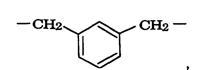 n representing an integer of 3 to 8. The bisallylnadimide is cured by
heating and exhibits excellent heat resistance.
n representing an integer of 3 to 8. The bisallylnadimide is cured by
heating and exhibits excellent heat resistance.
The thermosetting component of component (C) may be used singly
or in combination of two or more. The content of component (C) in the
photoresist composition is selected, in general, in the range of 1 to 20 parts
by weight and preferably in the range of 3 to 15 parts by weight per 100
parts by weight of the resin soluble in an alkali of component (A) from the
standpoint of the effect.
To provide the formed insulation film with the function of the light-shielding
film, where desired, the photoresist composition of the present
invention may further comprise at least one light-shielding material
selected from carbon black, chromium oxide, iron oxide, titanium black,
aniline black, black organic pigments and mixed organic pigments having
quasi-black color obtained by mixing at least two organic pigments
selected from red, blue, green, violet, yellow, cyan and magenta.
It is preferable that the light-shielding material is contained in the
photoresist composition in an amount of 20 to 80% by weight. Among the
above light-shielding materials, titanium black is preferable from the
standpoint of the light-shielding property.
To enhance the sensitivity, where desired, the photoresist
composition of the present invention may further comprise phenol
compounds such as polyhydroxybenzophenones described above, 1-[1-(4-hydroxyphenyl)isopropyl]-4-[1,1-bis(4-hydroxyphenyl)ethyl]benzene,
tris-(hydroxyphenyl)methanes and these compounds having methyl group as
the substituent; mercaptoxazole; mercaptobenzoxazole; mercaptoxazoline;
mercaptobenzothiazole; benzoxazoline; benzothiazolone; mercaptobenzimidazole;
urazole; thiourazole; mercaptopyrimidine; imidazolone;
and derivatives of these compounds.
As the auxiliary agent for improving the resolution and the fraction
of the residual film, the photoresist composition of the present invention
may further comprise isocyanurate-based compounds. Examples of the
isocyanurate-based compound include 1,3,5-tris(4-tert-butyl-3-hydroxy-2,6-dimethylbenzyl)
isocyanurate, 1,3,5-tris(4-tert-butyl-3-hydroxy-2;6-diethylbenzyl)
isocyanurate and 1,3,5-tris(3,5-di-tert-butyl-4-hydroxybenzyl)
isocyanurate.
Where necessary, the photoresist composition of the present
invention may further comprise additives compatible with the composition
such as additional resins, plasticizers, stabilizers and surfactants which
are conventionally used for improving the properties of the resist film.
The organic solvent used-in the resist-composition is not particularly
limited and a conventional solvent for photoresists can be used.
Examples of the organic solvent include linear chain ketones such as
acetone, methyl ethyl ketone, cyclopentanone, 2-hexanone, 3-hexanone, 2-heptanone,
3-heptanone, 4-heptanone, 2-octanone, 3-octanone and 4-octanone;
alcohols such as n-propyl alcohol, isopropyl alcohol, n-butyl
alcohol and cyclohexanol; ethers such as ethylene glycol dimethyl ether,
ethylene glycol diethyl ether and dioxane; alcohol ethers such as ethylene
glycol monomethyl ether and ethylene glycol monoethyl ether; esters such
as propyl formate, butyl formate, propyl acetate, butyl acetate, methyl
propionate, ethyl propionate, methyl butyrate, ethyl butyrate, methyl
lactate and ethyl lactate; cellosolve esters such as cellosolve acetate,
methylcellosolve acetate, ethylcellosolve acetate, propylcellosolve acetate
and butylcellosolve acetate; propylene glycols such as propylene glycol,
propylene glycol monomethyl ether, propylene glycol monomethyl ether
acetate, propylene glycol monoethyl ether acetate and propylene glycol
monobutyl ether; diethylene glycols such as diethylene glycol monomethyl
ether, diethylene glycol monoethyl ether, diethylene glycol dimethyl ether,
diethylene glycol diethyl ether and diethylene glycol methyl ethyl ether;
saturated γ-lactones such as γ-butyrolactone, γ-valerolactone, γ-caprolactone
and γ-caprylolactone; halogenated hydrocarbons such as
trichloroethylene; aromatic hydrocarbons such as toluene and xylene; and
polar solvents such as dimethylacetamide, dimethylformamide and N-methylacetamide.
The solvent may be used singly or in combination of
two or more. The amount of the solvent is not particularly limited as long
as the amount is sufficient for homogeneously dissolving or uniformly
dispersing the components described above.
The insulation film for organic EL devices of the present invention is
an insulation film which is formed by heating a resist film having a desired
pattern and formed with the photoresist composition described above on a
substrate in accordance with photolithography and has a sectional shape
having upper edge portions having a round shape and the width increasing
towards the bottom portion. It is preferable that the area of the portion of
the pattern contacting the substrate obtained after being heated is 140% or
smaller of the corresponding area before being heated. When the
downward increase in the sectional width [the area of the portion
contacting the substrate relative to the corresponding area before being
heated, (%)] exceeds 140%, the insulation film having the desired shape
and the desired thickness is not obtained, occasionally. When the
downward increase in the sectional width is small and the sectional shape
before being heated is a rectangle or close to a rectangle, the desired
sectional shape having the width increasing towards the bottom portion is
not obtained, occasionally. From the standpoints described above, it is
preferable that the downward increase in the sectional width is greater
than 100% and 140% or smaller and more preferably in the range of 102 to
130%.
The thickness of the insulation film is, in general, in the range of 0.3
to 3 µm, more preferably in the range of 0.5 to 2 µm and most preferably in
the range of 1 to 1.5 µm.
Figure 3 shows a diagram exhibiting an example of the change in
the shape when the resist film formed in accordance with the
photolithography is heated in the preparation of the insulation film of the
present invention. The portion surrounded by the solid line shows a front
view of the resist film having a rectangular sectional shape. The portion
surrounded by the broken line shows a front view of the insulation film of
the present invention obtained after heating the above resist film. The
downward increase in the sectional width is given by 100×(b/a)2.
As the substrate on which the insulation film for organic EL devices
of the present invention is formed, a transparent substrate having a
patterned transparent electrode layer (the anode) can be used.
As the transparent substrate, a flat and smooth substrate having a
transmittance of light in the visible region of 400 to 700 nm of 50% or
greater is preferable. Examples of the transparent substrate include
glass plates and polymer plates. Examples of the glass plate include
plates of soda lime glass, glass containing barium and strontium, lead
glass, aluminosilicate glass, borosilicate glass, barium borosilicate glass
and quartz. Examples of the polymer plate include plates of
polycarbonates, acrylic resins, polyethylene terephthalate, polyether
sulfite and polysulfone. Among these transparent substrates, in general,
glass plates are preferable.
As the anode, a transparent electrode using a metal, an alloy, an
electrically conductive compound or a mixture of these- materials which
has a great work function (4 eV or greater) as the electrode material is
preferable. It is preferable that the sheet resistance of the anode is
several hundred Ω/cm2 or smaller. Examples of the anode include
electrodes using an electrically conductive material such as ITO (indium
tin oxide), SnO2, ZnO and In-Zn-O as the electrode material. For forming
the anode, the electrode material is formed into a thin film in accordance
with the vapor deposition or the sputtering. The thickness of the anode is
selected, in general, in the range of 10 nm to 1 mm and preferably in the
range of 10 to 200 nm although the thickness depends on the type of the
material.
The insulation film for organic EL devices of the present invention
described above can be efficiently produced in accordance with the process
of the present invention shown in the following.
In the process of the present invention, a resist film having a
substantially rectangular sectional shape and a desired pattern is formed
with the photoresist composition described above on a substrate which is
specifically a transparent substrate having a patterned transparent
electrode layer (the anode) in accordance with the photolithography. The
formed resist film is heated at a temperature higher than the temperature
of heat resistance of the resist film so that the thermosetting component of
component (C) in the resist film is cured. The insulation film for organic
EL devices of the present having a sectional shape which has upper edge
portions having a round shape and the width increasing towards the
bottom portion can be obtained in this manner.
The process for producing the insulation film will be described
specifically in the following.
A transparent substrate having a patterned transparent electrode
layer (the anode) is coated with the photoresist composition described
above using a spinner or the like and the formed coating layer is dried to
form a photoresist layer. The thickness of the photoresist layer is
controlled so that the completed insulation film has the prescribed
thickness. The resultant laminate is irradiated with ultraviolet light,
deep UV or excimer laser beams by an apparatus for exposure with
demagnified projection via a desired mask pattern or is subjected to the
pattern drawing with electron beams. The treated laminate is then
heated. The heated laminate is developed with a developing liquid such
as an alkaline aqueous solution which is, for example, a 1 to 10% by weight
aqueous solution of tetramethylammonium hydroxide and a resist film
having the desired pattern and a substantially rectangular sectional shape
is formed.
The resist film formed as described above is heated at a temperature
higher than the temperature of heat resistance of the resist film by
preferably 5°C or greater and more preferably by 10°C or greater so that
the thermosetting component in the resist film is cured. It is important
that the temperature of the heating is controlled in accordance with the
temperature of heat resistance of the resist film and the temperature of
starting the curing of the thermosetting component so that the insulation
film having a sectional shape having upper edge portions having a round
shape and the width increasing towards the bottom portion is formed.
It is preferable that the temperature of heat resistance of the resist
film is in the range of 90 to 130°C and more preferably in the range of 95 to
125°C. When the temperature of heat resistance of the resist film is in
the above range and a thermosetting imide resin such as bisallylnadimide
is used as the thermosetting component, it is preferable that the
temperature of heating the resist film is in the range of 140 to 250°C and
more preferably in the range of 150 to 200°C. The time of the heating is
varied depending on the temperature of the heating and cannot be
generally decided. In general, the time of the heating in the range of
about 60 to 30 seconds is sufficient.
The insulation film for organic EL devices of the present invention
can be efficiently obtained as described above. Since the resist film has
been treated by heating at a high temperature, volatile components in the
film have been removed almost completely and do not adversely affect the
organic EL device.
The present invention also provides the organic EL device having
the resist film prepared as described above.
An embodiment of the process for producing the organic EL device of
the present invention will be described in the following.
As described above, a resist pattern layer is formed in accordance
with a conventional process via the insulation film of the present invention
which is formed on the transparent substrate having the patterned
transparent electrode (the anode) and has the sectional shape having the
width increasing towards the bottom portion. The resist pattern layer
may have a rectangular sectional shape or a undercut pattern profile.
When the resist pattern layer having a rectangular sectional shape
is formed, the photoresist used for forming the layer may be any of the
non-chemical amplification type and the chemical amplification type and
may be any of the positive type and the negative type. Examples of the
photoresist include (1) positive-type photoresists of the non-chemical
amplification type which comprise a novolak resin soluble in an alkali and
a compound having quinonediazide group as the essential components, (2)
positive-type photoresists of the chemical amplification type which
comprise a resin exhibiting change in solubility in an alkali by the action of
an acid and a compound generating an acid by irradiation with a radiation
as the essential components, and (3) negative type photoresists of the
chemical amplification type which comprise a resin soluble in an alkali, a
substance crosslinked with an acid and a compound generating an acid by
irradiation with a radiation as the essential components.
When the resist pattern layer having a undercut pattern profile is
formed, a photoresist such as that described in Japanese Patent No.
2989064 can be used. Examples of this photoresist include a negative
type photoresist which comprises at least one of (A) a component
crosslinked by exposure to light or by exposure to light, followed by a heat
treatment, (B) a resin soluble in an alkali and (C) a compound which
absorbs the light used for the exposure, and is developed by an alkaline
aqueous solution.
The process for forming the resist pattern layer using the above
photoresist is not particularly limited and the resist pattern layer having
the rectangular sectional shape or the undercut pattern profile can be
formed in accordance with the conventional lithography. The thickness of
the resist pattern layer is, in general, about 0.5 to several µm.
After the resist pattern layer is formed on the transparent substrate
having the patterned transparent electrode layer via the insulation film of
the present invention as described above, a hole injecting and transporting
layer is formed in accordance with the vacuum vapor deposition. The
conditions for the vacuum vapor deposition are different depending on the
used compound (the material of the hole injecting and transporting layer)
and the crystal structure and the recombination structure of the hole
injecting and transporting layer to be formed. In general, it is preferable
that the conditions are suitably selected in the following ranges: the
temperature of the source of vapor deposition: 50 to 450°C; the degree of
vacuum: 1×10⁻⁵ to 1×10⁻¹ Pa; the rate of vapor deposition: 0.01 to 50
nm/sec; the temperature of the substrate: -50 to 300°C; and the thickness
of the layer: 5 nm to 1 µm.
In the next step, an organic light emitting layer is formed on the
hole injecting and transporting layer in accordance with the vacuum vapor
deposition. In general, the conditions for the vacuum vapor deposition
can be selected in the same ranges as those described for the formation of
the hole injecting and transporting layer although the conditions are
different depending on the compounds used for the vacuum vapor
deposition. It is preferable that the thickness of the layer is in the range
of 10 to 40 nm.
On the light emitting layer thus formed, an electron injecting layer
is formed in accordance with the vacuum vapor deposition. The
conditions for the vacuum vapor deposition can be selected in the same
ranges as those described for the formation of the hole injecting and
transporting layer and the formation of the light emitting layer. It is
preferable that the thickness of the layer is in the range of 5 nm to 1 µm.
As the final step, the cathode is laminated in accordance with the
vacuum vapor deposition. The cathode is composed of a metal. It is
preferable that the thickness of the cathode is in the range of 50 to 200 nm.
A laminate (a light emitting portion) comprising the transparent
electrode layer (the anode), the organic EL material layer (the hole
injecting and transporting layer, the organic light emitting layer and the
electron injecting layer) and the metal electrode layer (the cathode) on the
transparent substrate is formed as described above.
Figure 4 shows a sectional view exhibiting the construction of an
embodiment of the light emitting portion in the organic EL device of the
present invention. On a transparent substrate 1 having a patterned
transparent electrode layer 2, resist pattern layers (resin separation
layers) 4 having a undercut pattern profile are disposed via the insulation
film of the present invention 3' having the sectional shape having the
width increasing towards the bottom portion. Between the resist pattern
layers, an organic EL material layer 5 (having the construction in which a
hole injecting and transporting layer, an organic light emitting layer and
an electron injecting layer are successively formed from the side of the
transparent electrode layer) having a metal electrode layer 6 on the
surface is disposed and a light emitting portion is formed. On the resist
pattern 4, an organic EL material layer 5a having a metal electrode layer
6a is formed due to convenience in the preparation although the organic
EL material layer 5a is not necessary from the standpoint of the function.
Since the insulation film 3' has, as shown in Figure 4, the shape
having the width increasing towards the bottom portion in the above
organic EL device, attachment of the metal electrode material to the
transparent electrode layer 2 due to the extended deposition of the metal
electrode material can be prevented during the lamination of the metal
electrode layer 6 in accordance with the vacuum vapor deposition.
Therefore, undesirable phenomena such as short circuit do not take place.
In addition to the above application of the insulation film of the
present invention to the organic EL device, the insulation film of the
present invention can also be used as a bank comprising an insulation film
disposed between holes in organic EL devices which are obtained by
forming organic EL material layers by injecting a macromolecular organic
EL material in accordance with the ink jet method.
In the above organic EL device, the organic light emitting layer has
the following functions: (1) the injecting function of injecting holes from the
anode or the hole injecting and transporting layer and injecting electrons
from the cathode or the electron injecting layer under application of an
electric field; (2) the transporting function of transporting the injected
charges (electrons and holes) by the force of the electric field; and (3) the
light emitting function of providing the field for recombination of electrons
and holes within the light emitting layer and leading the recombination to
light emission. The type of the light emitting material used in the light
emitting layer is not particularly limited and a material conventionally
used as the light emitting material in organic EL devices can be used.
Examples of the light emitting material include fluorescent whitening
agents such as benzothiazole-based agents, benzimidazole-based agents
and benzoxazole-based agents; metal chelate oxinoid compounds;
styrylbenzene-based compounds; distyrylpyrazine derivatives; and
aromatic dimethylidine compounds.
The hole injecting and transporting layer is a layer comprising a
hole transporting compound and has the function of transporting holes
injected from the anode to the light emitting layer. By-disposing the hole
injecting and transporting layer between the anode and the light emitting
layer, a greater amount of holes are injected into the light emitting layer
under a lower electric field. Moreover, electrons injected from the cathode
or the-electron injecting layer into the light emitting layer are accumulated
in the vicinity of the interface of the light emitting layer and the hole
injecting and transporting layer in the light emitting layer due to the
barrier for electrons existing at the interface. Thus, the efficiency of light
emission of the organic EL device is improved and the EL device exhibiting
the excellent light emitting property can be prepared. The hole
transporting compound used in the hole injecting and transporting layer is
not particularly limited and conventional compounds used heretofore as
the hole transporting compound in organic EL devices can be used.
Example of the hole transporting compound include triazole derivatives,
oxadiazole derivatives, imidazole derivatives, polyarylalkane derivatives,
pyrazoline derivatives, pyrazolone derivatives, phenylenediamine
derivatives, arylamine derivatives, amino-substituted chalcone derivatives,
oxazole derivatives, styrylanthracene derivatives, fluorenone derivatives,
hydrazone derivatives, stilbene derivatives, silazane derivatives,
polysilane derivatives, aniline-based copolymers and specific electrically
conductive macromolecular oligomers such as thiophene oligomers.
The electron injecting layer has the function of transporting
electrons injected from the cathode to the organic light emitting layer.
The electron transporting compound used in the electron injecting layer is
not particularly limited and conventional compounds used heretofore as
the electron transporting compound in organic EL devices can be used.
Example of the-electron transporting compound include nitro-substituted
fluorenone derivatives, anthraquinodimethane derivatives, diphenylquinone
derivatives, thiopyrane dioxide derivatives, heterocyclic
tetracarboxylic acid anhydrides such as corresponding compounds having
naphthalene ring or perylene ring, carbodiimides, fluorenylidenemethane
derivatives, anthrone derivatives, oxadiazole derivatives and metal
complexes of 8-quinolinol and derivatives thereof. Examples of the metal
complex of 8-quinolinol and the derivative thereof include tris(8-quinolinol)aluminum,
bis(8-quinolinol)magnesium, bis(benzo-8-quinolinol)zinc,
bis(2-methyl-8-quinolylato)aluminum oxide, tris(8-quinolinol)indium,
tris(5-methyl-8-quinolinol)aluminum, 8-quinolinol-lithium,
tris(5-chloro-8-quinolinol)potassium, bis(5-chloro-8-quinolinol)-potassium,
tris(5,7-dichloro-8-quinolinol)aluminum, tris(5,7-dibromo-8-quinolinol)aluminum,
bis(8-quinolinol)beryllium, bis(2-methyl-8-quinolinol)beryllium,
bis(8-quinolinol)zinc, bis(2-methyl-8-quinolinol)zinc,
bis(8-quinolinol)tin and tris(7-propyl-8-quinolinol)aluminum.
The organic light emitting layer, the hole injecting and transporting
layer and the electron injecting layer may be constituted with a single
layer comprising at least one material for the layer or may be a laminate of
at least two layers each comprising different materials.
As the cathode, a metal electrode comprising a metal, an alloy, an
electrically conductive compound or a mixture of these materials which
has a small work function (4 eV or smaller) as the electrode material is
used. Examples of the electrode material include sodium, sodium-potassium
alloys, magnesium, lithium, magnesium-silver alloys,
aluminum/aluminum oxide, indium and rare earth metals. It is
preferable that the sheet resistance as the electrode is several hundred
Ω/cm2 or smaller.
The present invention will be described more specifically with
reference to examples in the following. However, the present invention is
not limited to the examples.
A novolak resin having a weight-average molecular weight of 5,500,
which was obtained by condensation of a mixed cresol containing m-cresol
and p-cresol (the ratio of the mounts by weight: 50/50) and formaline in the
presence of oxalic acid as the catalyst, in an amount of 100 parts by weight,
22 parts by weight of 1,2-naphthoquinonediazide-4-sulfonic acid ester of
2,3,4-trihydroxybenzophenone (the fraction of esterification: 67% by mole),
5 parts by weight of a thermosetting imide resin "BANI-M" [a trade name;
manufactured by MARUZEN SEKIYU KAGAKU Co., Ltd.] and 450 parts
by weight of polyethylene glycol monomethyl ether acetate (PGMEA) were
mixed. After the components were completely dissolved, the resultant
solution was filtered through a membrane filter made of polytetrafluoroethylene
having pores having a diameter of 0.5 µm [manufactured by
MILLIPORE Company] and positive-type resist (A-1) was prepared.
To positive-type resist (A-1) obtained in Example 1, 30 parts by
weight (as pure titanium black) of titanium black treated for dispersion
with a polyester-based dispersant and 106 parts by weight of PGMEA per
100 parts by weight of the novolak resin in resist (A-1) were mixed. The
components were completely uniformly dispersed and positive-type resist
(A-2) was prepared.
A novolak resin having aweight-average molecular weight of 5,500,
which was obtained by condensation of a mixed cresol containing m-cresol
and p-cresol (the ratio of the amounts by weight: 50/50) and formaline in
the presence of oxalic acid as the catalyst, in an amount of 100 parts by
weight, 22 parts by weight of 1,2-naphthoquinonediazide-4-sulfonic acid
ester of 2,3,4-trihydroxybenzophenone (the average fraction of
esterification: 67% by mole) and 430 parts by weight of PGMEA were
mixed. After the components were completely dissolved, the resultant
solution was filtered through a membrane filter of polytetrafluoroethylene
having pores having a diameter of 0.5 µm [manufactured by MILLIPORE
Company] and positive-type resist (A-3) was prepared.
Positive-type resist (A-1) obtained in Example 1, positive-type resist
(A-2) obtained in Example 2 and positive-type resist (A-3) obtained in
Comparative Example 1 were each applied to a transparent glass
substrate using a spin coater each in an amount such that the formed
coating film had a thickness of 1.0 µm after being dried. The prepared
films were heated on a hot plate at 100°C for 90 seconds and photoresist
layers were formed.
The formed photoresist layers were exposed to light having an
energy of 120 mJ/cm2 using a light exposure apparatus "PLA501F"
[manufactured by CANON Co., Ltd.] via a mask to obtain latent images.
The exposed photoresist layers were treated by the paddle development in
a 2.38% by weight aqueous solution of tetramethylammonium hydroxide
for 60 seconds and resist films having a substantially rectangular sectional
shape were formed.
The photoresist films were then heated on a hot plate at the
temperature shown in Table 1 for 180 seconds and insulation films having
a sectional shape having the width increasing towards the bottom portion
were prepared. The downward increase in the sectional width
[100×(b/a)2, %] was obtained by using pictures of a scanning electron
microscope (SEM). The results are shown in Table 1.
| Positive-type resist | Downward increase in the sectional width | ||
| 150°C | 200°C | 250°C | |
| Example 1 (A-1) | 104% | 125% | 128% |
| Example 2 (A-2) | 108% | 117% | 114% |
| Comparative | 149% | 219% | - |
| Example 1 (A-3) |
As shown in Table 1, the insulation films of Examples 1 and 2 had
much smaller downward increases in the sectional width than that of the
insulation film of Comparative Example 1.
Upper edge portions of all insulation films had a round shape. The
specific permittivity measured in accordance with the method of Japanese
Industrial Standard C6481 was in the range of 3.3 to 3.5.
A glass substrate of a size of 25×75×1.1 mm which had on the
surface a patterned ITO transparent electrode having a thickness of 120
nm was coated with positive-type resist (A-2) obtained in Example 2 using
a spin coater in an amount such that the formed film had a thickness of 1.0
µm after being dried. The coating film was heated on a hot plate at 100°C
for 90 seconds and a resist layer was formed.
The formed resist layer was exposed to light having an energy of 120
mJ/cm2 using a light exposure apparatus "PLA501F" used above via a
mask having a desired pattern to obtain a latent image. The exposed
resist layer was treated by the paddle development in a 2.38% by weight
aqueous solution of tetramethylammonium hydroxide for 60 seconds. The
developed resist layer was heated on a hot plate at 200°C for 180 seconds
and an insulation film having a sectional shape having the width
increasing towards the bottom portion, in which the downward increase in
the sectional width was 117%, and a thickness of 1.0 µm was prepared.
A novolak resin having a weight-average molecular weight of 5,200,
which was obtained by polycondensation of a mixed-cresol containing m-cresol
and p-cresol (the ratio of the amounts by weight: 60/40) with
formaldehyde, in an amount of 100 parts by weight, 10 parts by weight of
hexamethoxymethylated melamine, 3 parts by weight of 2-(4-methoxy-naphthel)-4,6-bis(trichloromethyl)-s-triazine
and 3 parts by weight of 4-(4-dimethylaminophenylazo)phenol
were dissolved in 300 parts by weight of
ethylcellosolve acetate. The resultant solution was filtered through a
membrane filter and a photosensitive composition was prepared.
The glass substrate having the insulation film obtained in (1) was
coated with the above composition in accordance with the spin coating.
The formed coating film was heated on a hot plate at 90°C for 60 seconds
and a resist film having a thickness of 1.5 µm was formed.
The resist film was exposed to light using the light exposure
apparatus "PLA501F" used above via a mask having a desired pattern and
treated by the paddle development in a 0.5% by weight aqueous solution of
NaOH for 60 seconds. Due to the above operation, a resist pattern having
a undercut pattern profile was formed on the insulation film. The resist
pattern was irradiated with light by using a high pressure mercury lamp
having a brightness at 254 nm of 1.2 mW/cm2 for 200 seconds to bake the
resist pattern and a member for an organic EL device was prepared.
The member for an organic EL device prepared in (2) described
above was used as the substrate and fixed at a substrate holder of a
commercial vapor deposition apparatus [manufactured by NIPPON
SHINKU GIJUTU Co., Ltd.]. Into a boated made of molybdenum and
heated by resistance, 200 mg of N,N'-bis(3-methylphenyl)-N,N'-diphenyl-[1.1'-biphenyl]-4,4'-diamine
(hereinafter, referred to as TPD) was placed
and 200 mg of 4,4'-bis(2,2'-diphenylvinyl)biphenyl (hereinafter, referred to
as DPVBi) was placed into another boated made of molybdenum and
heated by resistance. The vacuum chamber was evacuated to 1×10⁻⁴ Pa.
TPD was vapor deposited at a rate of vapor deposition of 0.1 to 0.3
nm/sec by heating the boat containing TPD at 215 to 220°C and a hole
injecting and- transporting layer having a thickness of 60 nm was formed.
During this formation, the temperature of the substrate was kept at the
room temperature. Without taking out the coated substrate, DPVBi was
vapor deposited on the formed hole injecting and transporting layer at a
rate of vapor deposition of 0.1 to 0.3 nm/sec by heating the boat containing
DPVBi at 240°C and a light emitting layer having a thickness of 40 nm
was formed. During this formation, the temperature of the substrate was
kept at the room temperature.
The resultant product was taken out of the vacuum chamber. After
a mask made of stainless steel was placed on the light emitting layer
formed above, the product was fixed at the substrate holder again. Into a
boat made of molybdenum, 200 mg of tris(8-quinolinol)aluminum
(hereinafter, referred to as Alq3) was placed and 1 g of magnesium ribbon
was placed into another boat made of molybdenum. Into a basket made of
tungsten, 500 mg of silver wire was placed. The boats and the basket
were placed into the vacuum chamber.
After the vacuum chamber was evacuated to 1×10⁻⁴ Pa, Alq3 was
vapor deposited on the light emitting layer formed above at a rate of vapor
deposition of 0.01 to 0.03 nm/sec by heating the boat containing Alq3 at
230°C and an electron injecting layer having a thickness of 20 nm was
formed. On the formed electron injecting layer, silver was vapor
deposited at a rate of vapor deposition of 0.1 nm/sec and, simultaneously,
magnesium was vapor deposited at a rate of vapor deposition of 1.4 nm/sec.
Thus, a cathode composed of a mixed metal of magnesium and silver and
having a thickness of 150 nm was formed and a light emitting portion of an
organic EL device shown in Figure 4 was formed.
Then, a sealing layer was formed in accordance with the
conventional process and an organic EL device was prepared.
When a direct current was applied to the device using the ITO film
as the anode and the mixed metal film as the cathode, emission of blue
light could be recognized in a bright environment under a voltage of 5 V or
greater and the self-distinguishability was found to be very excellent.
The photoresist composition of the present invention comprises a
thermosetting component which is cured at a specific temperature and
provides the insulation film which has a sectional shape having upper edge
portions having a round shape and the width increasing towards the
bottom portion and is advantageous as the insulation film for organic EL
devices.
By using the above insulation film, the organic EL device can be
produced with stability and suppressed formation of defect products.
Claims (6)
- A photoresist composition for forming an insulation film for organic electroluminescence devices which comprises (A) a resin soluble in an alkali, (B) an ester of a quinonediazidesulfonic acid, (C) a thermosetting component which is cured at a temperature higher than a temperature of heat resistance of a resist film formed with the composition in accordance with photolithography, and an organic solvent.
- A photoresist composition for forming an insulation film according to Claim 1, wherein the thermosetting component of component (C) is a thermosetting imide resin represented by general formula [1]:wherein R represents a group expressed by:

 n representing an integer of 3 to 8.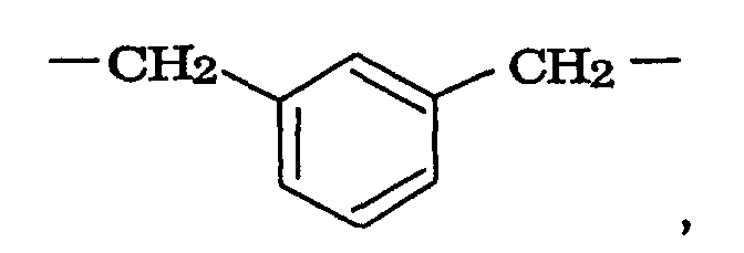
- A photoresist composition for forming an insulation film according to any one of Claims 1 and 2, which comprises 1 to 20 parts by weight of component (C) per 100 parts by weight of component (A).
- An insulation film for organic electroluminescence devices which is formed by heating a resist film having a desired pattern and formed with a composition described in any one of Claims 1, 2 and 3 on a substrate in accordance with photolithography, has a sectional shape having upper edge portions having a round shape and a width increasing towards a bottom portion and has a thickness in a range of 0.3 to 3 µm.
- A process for producing an insulation film for organic electroluminescence devices described in Claim 4, the process comprising forming a resist film having a substantially rectangular sectional shape and a desired pattern with a photoresist composition described in any one of Claims 1, 2 and 3 on a substrate in accordance with photolithography and heating the formed resist film at a temperature higher than a temperature of heat resistance of the resist film so that the thermosetting component in the resist film is cured.
- An organic electroluminescence device which comprises an insulation film described in Claim 4.
Applications Claiming Priority (3)
| Application Number | Priority Date | Filing Date | Title |
|---|---|---|---|
| JP2000298678 | 2000-09-29 | ||
| JP2000298678 | 2000-09-29 | ||
| PCT/JP2001/004883 WO2002029493A1 (en) | 2000-09-29 | 2001-06-08 | Photoresist composition for forming insulation film, insulation film for organic electroluminescence element and method for its formation |
Publications (2)
| Publication Number | Publication Date |
|---|---|
| EP1321821A1 true EP1321821A1 (en) | 2003-06-25 |
| EP1321821A4 EP1321821A4 (en) | 2004-06-23 |
Family
ID=18780609
Family Applications (1)
| Application Number | Title | Priority Date | Filing Date |
|---|---|---|---|
| EP01936938A Withdrawn EP1321821A4 (en) | 2000-09-29 | 2001-06-08 | PHOTOSENSITIVE RESIN COMPOSITION FOR CREATING AN INSULATING LAYER, INSULATING LAYER OF ORGANIC ELECTROLUMINESCENT ELEMENTS AND METHOD OF CREATING |
Country Status (5)
| Country | Link |
|---|---|
| US (1) | US7008883B2 (en) |
| EP (1) | EP1321821A4 (en) |
| KR (1) | KR20040004383A (en) |
| TW (1) | TW594395B (en) |
| WO (1) | WO2002029493A1 (en) |
Cited By (2)
| Publication number | Priority date | Publication date | Assignee | Title |
|---|---|---|---|---|
| US7560863B2 (en) * | 2004-04-19 | 2009-07-14 | Lg Display Co., Ltd. | Organic electroluminescent display device including a shielding pattern to reduce resistance |
| US8609181B2 (en) | 2003-06-16 | 2013-12-17 | Semiconductor Energy Laboratory Co., Ltd. | Light emitting device and method for fabricating light emitting device |
Families Citing this family (40)
| Publication number | Priority date | Publication date | Assignee | Title |
|---|---|---|---|---|
| JP2005512298A (en) * | 2001-12-10 | 2005-04-28 | コーニンクレッカ フィリップス エレクトロニクス エヌ ヴィ | EL display device and method of manufacturing the same |
| JP3843995B2 (en) * | 2002-05-27 | 2006-11-08 | 日本ゼオン株式会社 | Radiation sensitive resin composition, method for producing substrate having patterned resin film, and use of the resin composition |
| GB2421117B (en) * | 2002-09-17 | 2006-09-27 | Dainippon Printing Co Ltd | Method of manufacturing a light emitting display panel and a light emitting diplay panel |
| JP4556757B2 (en) * | 2004-06-23 | 2010-10-06 | 日立電線株式会社 | Manufacturing method of semiconductor device |
| KR100682905B1 (en) * | 2004-12-01 | 2007-02-15 | 삼성전자주식회사 | Method of manufacturing unidirectional transparent optical system |
| DE102004063416A1 (en) * | 2004-12-23 | 2006-07-06 | Az Electronic Materials (Germany) Gmbh | Process for the preparation of a photoresist solution |
| KR100729256B1 (en) * | 2005-01-13 | 2007-06-15 | 삼성전자주식회사 | Photoresist composition, method for forming a photoresist pattern and method for forming a protection layer of a semiconductor device using the photoresist composition |
| KR101142999B1 (en) * | 2005-02-03 | 2012-05-08 | 주식회사 삼양이엠에스 | Photoresist composition, method for forming a pattern using the same, and method for manufacturing thin film transistor array panel using the same |
| KR100858823B1 (en) * | 2007-05-30 | 2008-09-17 | 삼성에스디아이 주식회사 | Organic light emitting display |
| KR101113063B1 (en) * | 2008-05-22 | 2012-02-15 | 주식회사 엘지화학 | Photosensitive resin composition containing polyimide and novolak resin |
| JP5079089B2 (en) * | 2008-05-29 | 2012-11-21 | 旭化成イーマテリアルズ株式会社 | Photosensitive resin composition, method for producing cured relief pattern, and semiconductor device |
| KR101288640B1 (en) * | 2008-05-29 | 2013-07-22 | 아사히 가세이 이-매터리얼즈 가부시키가이샤 | Photosensitive resin composition |
| TWI475124B (en) | 2009-05-22 | 2015-03-01 | Samsung Display Co Ltd | Thin film deposition apparatus |
| JP5620146B2 (en) | 2009-05-22 | 2014-11-05 | 三星ディスプレイ株式會社Samsung Display Co.,Ltd. | Thin film deposition equipment |
| KR101074792B1 (en) * | 2009-06-12 | 2011-10-19 | 삼성모바일디스플레이주식회사 | Thin film deposition apparatus |
| JP5328726B2 (en) * | 2009-08-25 | 2013-10-30 | 三星ディスプレイ株式會社 | Thin film deposition apparatus and organic light emitting display device manufacturing method using the same |
| JP5677785B2 (en) * | 2009-08-27 | 2015-02-25 | 三星ディスプレイ株式會社Samsung Display Co.,Ltd. | Thin film deposition apparatus and organic light emitting display device manufacturing method using the same |
| US20110052795A1 (en) * | 2009-09-01 | 2011-03-03 | Samsung Mobile Display Co., Ltd. | Thin film deposition apparatus and method of manufacturing organic light-emitting display device by using the same |
| US8876975B2 (en) | 2009-10-19 | 2014-11-04 | Samsung Display Co., Ltd. | Thin film deposition apparatus |
| KR101084184B1 (en) * | 2010-01-11 | 2011-11-17 | 삼성모바일디스플레이주식회사 | Thin film deposition apparatus |
| KR101174875B1 (en) * | 2010-01-14 | 2012-08-17 | 삼성디스플레이 주식회사 | Apparatus for thin layer deposition, method for manufacturing of organic light emitting display apparatus using the same, and organic light emitting display apparatus manufactured by the method |
| KR101193186B1 (en) | 2010-02-01 | 2012-10-19 | 삼성디스플레이 주식회사 | Apparatus for thin layer deposition, method for manufacturing of organic light emitting display apparatus using the same, and organic light emitting display apparatus manufactured by the method |
| KR101156441B1 (en) * | 2010-03-11 | 2012-06-18 | 삼성모바일디스플레이주식회사 | Apparatus for thin layer deposition |
| KR101202348B1 (en) | 2010-04-06 | 2012-11-16 | 삼성디스플레이 주식회사 | Apparatus for thin layer deposition and method for manufacturing of organic light emitting display apparatus using the same |
| US8894458B2 (en) | 2010-04-28 | 2014-11-25 | Samsung Display Co., Ltd. | Thin film deposition apparatus, method of manufacturing organic light-emitting display device by using the apparatus, and organic light-emitting display device manufactured by using the method |
| KR101223723B1 (en) | 2010-07-07 | 2013-01-18 | 삼성디스플레이 주식회사 | Apparatus for thin layer deposition, method for manufacturing of organic light emitting display apparatus using the same, and organic light emitting display apparatus manufactured by the method |
| KR101723506B1 (en) | 2010-10-22 | 2017-04-19 | 삼성디스플레이 주식회사 | Apparatus for organic layer deposition and method for manufacturing of organic light emitting display apparatus using the same |
| KR101738531B1 (en) | 2010-10-22 | 2017-05-23 | 삼성디스플레이 주식회사 | Method for manufacturing of organic light emitting display apparatus, and organic light emitting display apparatus manufactured by the method |
| KR20120045865A (en) | 2010-11-01 | 2012-05-09 | 삼성모바일디스플레이주식회사 | Apparatus for organic layer deposition |
| KR20120065789A (en) | 2010-12-13 | 2012-06-21 | 삼성모바일디스플레이주식회사 | Apparatus for organic layer deposition |
| KR101760897B1 (en) | 2011-01-12 | 2017-07-25 | 삼성디스플레이 주식회사 | Deposition source and apparatus for organic layer deposition having the same |
| KR101840654B1 (en) | 2011-05-25 | 2018-03-22 | 삼성디스플레이 주식회사 | Apparatus for organic layer deposition and method for manufacturing of organic light emitting display apparatus using the same |
| KR101852517B1 (en) | 2011-05-25 | 2018-04-27 | 삼성디스플레이 주식회사 | Apparatus for organic layer deposition and method for manufacturing of organic light emitting display apparatus using the same |
| KR101857249B1 (en) | 2011-05-27 | 2018-05-14 | 삼성디스플레이 주식회사 | Patterning slit sheet assembly, apparatus for organic layer deposition, method for manufacturing organic light emitting display apparatus and organic light emitting display apparatus |
| KR101826068B1 (en) | 2011-07-04 | 2018-02-07 | 삼성디스플레이 주식회사 | Apparatus for thin layer deposition |
| KR101901046B1 (en) | 2011-12-09 | 2018-09-20 | 아사히 가세이 이-매터리얼즈 가부시키가이샤 | Photosensitive resin composition, method for producing hardened relief pattern, semiconductor device and display device |
| JP5851307B2 (en) * | 2012-03-29 | 2016-02-03 | 東京応化工業株式会社 | Method for producing photosensitive substrate composition for forming light shielding layer |
| TWI490653B (en) * | 2013-09-10 | 2015-07-01 | Chi Mei Corp | Positive photosensitive resin composition and method for forming patterns by using the same |
| KR102602193B1 (en) * | 2016-08-12 | 2023-11-15 | 삼성디스플레이 주식회사 | Organic light-emitting apparatus and the method for manufacturing of the organic light-emitting display apparatus |
| KR102894308B1 (en) * | 2019-07-31 | 2025-12-02 | 엘지디스플레이 주식회사 | Display apparatus having a substrate hole |
Family Cites Families (14)
| Publication number | Priority date | Publication date | Assignee | Title |
|---|---|---|---|---|
| DE69033938T2 (en) * | 1989-12-01 | 2002-07-18 | Tosoh Corp., Shinnanyo | Positive working photosensitive compositions for the production of lenses |
| JP3241399B2 (en) * | 1991-05-30 | 2001-12-25 | ジェイエスアール株式会社 | Radiation-sensitive resin composition for microlenses |
| US5362597A (en) * | 1991-05-30 | 1994-11-08 | Japan Synthetic Rubber Co., Ltd. | Radiation-sensitive resin composition comprising an epoxy-containing alkali-soluble resin and a naphthoquinone diazide sulfonic acid ester |
| JPH07140648A (en) * | 1993-11-18 | 1995-06-02 | Tosoh Corp | Thermosetting photosensitive material |
| JPH09143420A (en) * | 1995-09-21 | 1997-06-03 | Asahi Glass Co Ltd | Low dielectric constant resin composition |
| JPH09278849A (en) * | 1996-04-12 | 1997-10-28 | Nippon Kayaku Co Ltd | Resin composition, resist ink resin composition and cured product thereof |
| JPH09325210A (en) * | 1996-05-31 | 1997-12-16 | Nippon Kayaku Co Ltd | Resin composition, resin composition for color filter protective film and its hardened material |
| JP3228183B2 (en) * | 1996-12-02 | 2001-11-12 | 日本電気株式会社 | Insulating film, semiconductor device having the insulating film, and method of manufacturing the same |
| US6104092A (en) * | 1997-04-02 | 2000-08-15 | Nec Corporation | Semiconductor device having amorphous carbon fluoride film of low dielectric constant as interlayer insulation material |
| JP4166355B2 (en) * | 1999-03-08 | 2008-10-15 | 出光興産株式会社 | Resin composition for fluorescent conversion film, fluorescent conversion film and colored organic electroluminescence device |
| JP2001005175A (en) * | 1999-06-23 | 2001-01-12 | Victor Co Of Japan Ltd | Photoresist for information recoding medium |
| JP2001234163A (en) * | 2000-02-25 | 2001-08-28 | Sony Corp | Light-emitting crystal particles, light-emitting crystal particle composition, display panel, and flat display device |
| US6984476B2 (en) * | 2002-04-15 | 2006-01-10 | Sharp Kabushiki Kaisha | Radiation-sensitive resin composition, forming process for forming patterned insulation film, active matrix board and flat-panel display device equipped with the same, and process for producing flat-panel display device |
| JP2004152920A (en) * | 2002-10-30 | 2004-05-27 | Fujitsu Ltd | Semiconductor device manufacturing method and semiconductor manufacturing process management method |
-
2001
- 2001-05-29 TW TW090112882A patent/TW594395B/en not_active IP Right Cessation
- 2001-06-08 US US10/381,432 patent/US7008883B2/en not_active Expired - Lifetime
- 2001-06-08 EP EP01936938A patent/EP1321821A4/en not_active Withdrawn
- 2001-06-08 WO PCT/JP2001/004883 patent/WO2002029493A1/en not_active Ceased
- 2001-06-08 KR KR10-2003-7004427A patent/KR20040004383A/en not_active Abandoned
Cited By (3)
| Publication number | Priority date | Publication date | Assignee | Title |
|---|---|---|---|---|
| US8609181B2 (en) | 2003-06-16 | 2013-12-17 | Semiconductor Energy Laboratory Co., Ltd. | Light emitting device and method for fabricating light emitting device |
| US7560863B2 (en) * | 2004-04-19 | 2009-07-14 | Lg Display Co., Ltd. | Organic electroluminescent display device including a shielding pattern to reduce resistance |
| US7902753B2 (en) | 2004-04-19 | 2011-03-08 | Lg Display Co., Ltd. | Organic electroluminescent display device and fabricating method thereof |
Also Published As
| Publication number | Publication date |
|---|---|
| US20040096771A1 (en) | 2004-05-20 |
| TW594395B (en) | 2004-06-21 |
| EP1321821A4 (en) | 2004-06-23 |
| US7008883B2 (en) | 2006-03-07 |
| WO2002029493A1 (en) | 2002-04-11 |
| KR20040004383A (en) | 2004-01-13 |
Similar Documents
| Publication | Publication Date | Title |
|---|---|---|
| US7008883B2 (en) | Photoresist composition for forming an insulation film, insulation film for organic electroluminescence devices and process for producing the insulation film | |
| JP4438080B2 (en) | Radiation-sensitive resin composition for forming insulating film and insulating film for organic electroluminescence device | |
| JP4857521B2 (en) | Electro-optical device manufacturing method, electro-optical device, and electronic apparatus | |
| JP6841242B2 (en) | Organic EL display device | |
| CN103543607B (en) | Organic EL element, radiation sensitive linear resin composition and cured film | |
| KR20140007799A (en) | Photosensitive resin composition, patterned structure, display device, and partition wall | |
| JP2001281440A (en) | Light-shielding film, method for producing the same and use thereof | |
| WO2014069091A1 (en) | Photosensitive resin composition, cured film, protective film, insulating film, and electronic device | |
| KR100773281B1 (en) | Resist Composition and Resist Pattern Forming Method | |
| JP2015187668A (en) | Photosensitive resin composition, cured film, protection film, insulator film, and electronic equipment | |
| JP4513965B2 (en) | Radiation sensitive resin composition | |
| KR102928583B1 (en) | Organic EL display device | |
| KR102926281B1 (en) | Organic EL display device, method for manufacturing a cured product, and method for manufacturing an organic EL display device | |
| KR20170054496A (en) | Light emitting device and manufacturing method for same, manufacturing method for barrier, and radiation-sensitive material | |
| KR101115787B1 (en) | Positive type resist, insulating layer and OLED | |
| JP2006179423A (en) | Negative-type radiation-sensitive resin composition and insulating film of organic electroluminescence display device using the same | |
| KR20240110932A (en) | Photosensitive resin composition, cured product, organic EL display device, semiconductor device, and method for producing the cured product | |
| JP4507277B2 (en) | Pattern formation method | |
| JP2006133585A (en) | Radiation sensitive resin composition and method for forming radiation sensitive resin pattern | |
| KR102930981B1 (en) | Curable composition, cured film, organic el device, and method for forming cured resin layer | |
| JP2006201653A (en) | Radiation sensitive resin composition for insulating film formation | |
| JP2023145369A (en) | image display device | |
| EP4737506A1 (en) | Cured film and organic el display device | |
| KR20240015965A (en) | Cured film, photosensitive resin composition forming the same and display device | |
| KR20240161633A (en) | Photosensitive resin composition, cured product, method for producing cured product, organic EL display device and display device |
Legal Events
| Date | Code | Title | Description |
|---|---|---|---|
| PUAI | Public reference made under article 153(3) epc to a published international application that has entered the european phase |
Free format text: ORIGINAL CODE: 0009012 |
|
| 17P | Request for examination filed |
Effective date: 20030331 |
|
| AK | Designated contracting states |
Designated state(s): AT BE CH CY DE DK ES FI FR GB GR IE IT LI LU MC NL PT SE TR |
|
| RBV | Designated contracting states (corrected) |
Designated state(s): DE FR GB |
|
| A4 | Supplementary search report drawn up and despatched |
Effective date: 20040512 |
|
| RAP1 | Party data changed (applicant data changed or rights of an application transferred) |
Owner name: ZEON CORPORATION |
|
| 17Q | First examination report despatched |
Effective date: 20070309 |
|
| STAA | Information on the status of an ep patent application or granted ep patent |
Free format text: STATUS: THE APPLICATION IS DEEMED TO BE WITHDRAWN |
|
| 18D | Application deemed to be withdrawn |
Effective date: 20070720 |