EP1320130A2 - Semiconductor device and manufcaturing method thereof - Google Patents
Semiconductor device and manufcaturing method thereof Download PDFInfo
- Publication number
- EP1320130A2 EP1320130A2 EP02252913A EP02252913A EP1320130A2 EP 1320130 A2 EP1320130 A2 EP 1320130A2 EP 02252913 A EP02252913 A EP 02252913A EP 02252913 A EP02252913 A EP 02252913A EP 1320130 A2 EP1320130 A2 EP 1320130A2
- Authority
- EP
- European Patent Office
- Prior art keywords
- conductive
- semiconductor film
- film
- type
- region
- Prior art date
- Legal status (The legal status is an assumption and is not a legal conclusion. Google has not performed a legal analysis and makes no representation as to the accuracy of the status listed.)
- Granted
Links
Images




Classifications
-
- H—ELECTRICITY
- H10—SEMICONDUCTOR DEVICES; ELECTRIC SOLID-STATE DEVICES NOT OTHERWISE PROVIDED FOR
- H10D—INORGANIC ELECTRIC SEMICONDUCTOR DEVICES
- H10D84/00—Integrated devices formed in or on semiconductor substrates that comprise only semiconducting layers, e.g. on Si wafers or on GaAs-on-Si wafers
- H10D84/01—Manufacture or treatment
- H10D84/0112—Integrating together multiple components covered by H10D8/00, H10D10/00 or H10D18/00, e.g. integrating multiple BJTs
- H10D84/0119—Integrating together multiple components covered by H10D8/00, H10D10/00 or H10D18/00, e.g. integrating multiple BJTs the components including complementary BJTs
-
- H—ELECTRICITY
- H10—SEMICONDUCTOR DEVICES; ELECTRIC SOLID-STATE DEVICES NOT OTHERWISE PROVIDED FOR
- H10D—INORGANIC ELECTRIC SEMICONDUCTOR DEVICES
- H10D84/00—Integrated devices formed in or on semiconductor substrates that comprise only semiconducting layers, e.g. on Si wafers or on GaAs-on-Si wafers
- H10D84/01—Manufacture or treatment
- H10D84/0123—Integrating together multiple components covered by H10D12/00 or H10D30/00, e.g. integrating multiple IGBTs
- H10D84/0126—Integrating together multiple components covered by H10D12/00 or H10D30/00, e.g. integrating multiple IGBTs the components including insulated gates, e.g. IGFETs
- H10D84/0165—Integrating together multiple components covered by H10D12/00 or H10D30/00, e.g. integrating multiple IGBTs the components including insulated gates, e.g. IGFETs the components including complementary IGFETs, e.g. CMOS devices
- H10D84/0172—Manufacturing their gate conductors
- H10D84/0177—Manufacturing their gate conductors the gate conductors having different materials or different implants
-
- H—ELECTRICITY
- H10—SEMICONDUCTOR DEVICES; ELECTRIC SOLID-STATE DEVICES NOT OTHERWISE PROVIDED FOR
- H10D—INORGANIC ELECTRIC SEMICONDUCTOR DEVICES
- H10D84/00—Integrated devices formed in or on semiconductor substrates that comprise only semiconducting layers, e.g. on Si wafers or on GaAs-on-Si wafers
- H10D84/01—Manufacture or treatment
- H10D84/0123—Integrating together multiple components covered by H10D12/00 or H10D30/00, e.g. integrating multiple IGBTs
- H10D84/0126—Integrating together multiple components covered by H10D12/00 or H10D30/00, e.g. integrating multiple IGBTs the components including insulated gates, e.g. IGFETs
- H10D84/0165—Integrating together multiple components covered by H10D12/00 or H10D30/00, e.g. integrating multiple IGBTs the components including insulated gates, e.g. IGFETs the components including complementary IGFETs, e.g. CMOS devices
- H10D84/0186—Manufacturing their interconnections or electrodes, e.g. source or drain electrodes
-
- H—ELECTRICITY
- H10—SEMICONDUCTOR DEVICES; ELECTRIC SOLID-STATE DEVICES NOT OTHERWISE PROVIDED FOR
- H10D—INORGANIC ELECTRIC SEMICONDUCTOR DEVICES
- H10D84/00—Integrated devices formed in or on semiconductor substrates that comprise only semiconducting layers, e.g. on Si wafers or on GaAs-on-Si wafers
- H10D84/01—Manufacture or treatment
- H10D84/02—Manufacture or treatment characterised by using material-based technologies
- H10D84/03—Manufacture or treatment characterised by using material-based technologies using Group IV technology, e.g. silicon technology or silicon-carbide [SiC] technology
- H10D84/038—Manufacture or treatment characterised by using material-based technologies using Group IV technology, e.g. silicon technology or silicon-carbide [SiC] technology using silicon technology, e.g. SiGe
Definitions
- the present invention relates to a semiconductor device and a manufacturing method thereof, and, in particular, the present invention is best suited when applied to a semiconductor device provided with a gate electrode including silicide.
- a laminated structure of polysilicon and silicide is adopted, and a dual structure in which a gate of NMOS transistor is an N-type and a gate of PMOS transistor is a P-type is adopted.
- Figs. 13A, 13B, and 13C, and Figs. 14A, and 14B are diagrammatic sectional views showing a manufacturing method of a conventional CMOS transistor adopting the above-described dual gate structure in the order of its processes.
- a field oxide film 72 and gate oxide films 73a and 73b on a silicon substrate 71
- a non-doped polysilicon film is laminated.
- a resist mask 75 is formed in a region to form a gate and the non-doped polysilicon film is patterned using the resist mask 75 as a mask to form a polysilicon film 74 for forming the gate.
- the resist mask 75 is removed, a resist mask 76 is newly formed on the polysilicon film 74 which is positioned in a PMOS forming region, and ion implantation with an arsenic ion (As + ) is performed using the resist mask 76 as a mask.
- a boron ion (B + ) is injected into the PMOS side to form source and drain regions in high concentration in the PMOS forming region.
- a silicon substrate 71 is heated to activate the impurity injected with the ions.
- silicide 80 is formed in the gate electrode, and source and drain regions using a high melting point metal.
- the resist masks 76 to 79 which are used for formation of a CMOS transistor as described above are generally made of a polymer compound.
- carbide which composes the resist masks 76 to 79 is driven into the surface of the polysilicon film 74 positioned in the edge portion of the resist mask.
- silicide is considered not to be formed in the regions 81a and 81b where the carbide remains, due to the inhibition of silicide formation, which is disadvantageous in that a semiconductor device can not perform a predetermined operation.
- a semiconductor device comprises a semiconductor film formed above a semiconductor substrate (the semiconductor film having doped parts) and a silicide film formed on the above-described semiconductor film, wherein at least one out of the same (first) conductive (conductivity type) semiconductor film(s) (part) formed above the semiconductor substrate is connected including one, two or more differences in (ion) concentration along the surface of the semiconductor substrate.
- a region where the silicide film is not formed is on a region having the above-described difference in concentration.
- references herein to films include film parts, for example forming separate parts of the same layer in a semiconductor device.
- the above-described semiconductor film comprises a first conductive-type semiconductor film (or doped part) having two or more differences in concentration and a second conductive-type semiconductor film (or doped part) different from the first conductive-type, wherein a region (or portion) of low concentration on the first conductive-type semiconductor film is connected to the second conductive-type semiconductor film. Then, it is preferable because the region where the silicide film is not formed does not overlap with the junction of different conductive-type semiconductor films when forming a first conductive-type transistor.
- the above-described semiconductor film may specifically comprise the first conductive-type semiconductor film having two or more differences in concentration, the second conductive-type semiconductor film different from the first conductive-type, and a non-doped semiconductor film in which an impurity is not doped, wherein the non-doped semiconductor film is connectedly sandwiched between the region of low concentration in the first conductive-type semiconductor film and the second conductive-type semiconductor film along the surface of the semiconductor substrate. Then, it is more preferable because the impurity of the first conductive-type and the impurity of the second conductive-type can be injected in any concentration.
- the above-described semiconductor film may concretely comprise the first conductive-type semiconductor film having two or more differences in concentration, and the second conductive-type semiconductor film having two or more differences in concentration and different from the first conductive-type, wherein a region of low concentration in the first conductive-type semiconductor film is connected with a region of low concentration in the second conductive-type semiconductor film. Then, it is preferable because the silicide film non-forming region does not overlap with the junction of different conductive-type semiconductor films when forming a second conductive-type transistor.
- an impurity in high concentration of the semiconductor film which is heavier in mass than the impurity existing in the region of low concentration in the semiconductor film.
- a semiconductor device may comprise an insulation film formed on the surface of the semiconductor substrate and diffusion layers formed in the semiconductor substrate in a manner to sandwich a lower region of the same conductive-type semiconductor film so as to form a transistor in which the semiconductor film serves as a gate, the insulation film serves as a gate insulation film, and the diffusion layers serve as a source and a drain.
- the semiconductor film may be, for instance, a polysilicon film.
- a manufacturing method of a semiconductor device comprises: a first step of forming a semiconductor film above a semiconductor substrate; a second step of forming a first mask layer covering a partial region of the semiconductor film; a third step of forming a first conductive-type semiconductor film in said semiconductor film by injecting a first impurity in a first conductive-type into the semiconductor film using said first mask layer as a mask; a fourth step of removing the first mask layer; a fifth step of forming a second mask layer covering a partial region of the first conductive-type semiconductor film and a semiconductor film different from the first conductive-type semiconductor film to include the boundary region between the first conductive-type semiconductor film and a semiconductor film different from the first conductive semiconductor film; a sixth step of forming the first conductive-type semiconductor film of high concentration and the first conductive-type semiconductor film of low concentration by injecting the second impurity of the same conductive type as said first conductive type, composing of a heavier element in mass than said first
- the manufacturing method of the semiconductor device comprises: a first step of forming a region of low concentration in the same conductive-type semiconductor film by injecting an impurity ion of a light element in at least one semiconductor film of the same conductive type out of the gate semiconductor films; a second step of forming a region of high concentration in the same conductive-type semiconductor film by injecting an impurity ion of a heavy element heavier in mass than the light element into a lower concentration region side with respect to the junction between the two different conductive-type semiconductor films out of the same conductive-type semiconductor films; and a third step of forming a silicide film on the junction between the two different conductive-type semiconductor films, so that the silicide film non-forming region does not overlap with the junction between the two different conductive-type
- a semiconductor device in which a semiconductor film has a doped part of a first conductivity type formed with at least one difference in ion concentration.
- a silicide layer may be formed over the film and a silicide non-forming region does not overlap with a pn junction of the semiconductor device.
- semiconductor (eg polysilicon) films are covered with a resist mask so as to cover an end of the resist mask covering the polysilicon films to form a PMOS forming region.
- a silicide non-forming region is arranged not to overlap with a pn junction to prevent the silicide non-forming region from increasing in resistance.
- the inventors of the present invention studied the effect of different ions injected into polysilicon on the silicide formed thereafter on the polysilicon, in detail. As a result, the following important fact was found.
- the inventors of the present invention have found that the silicide formed on polysilicon depends largely on the kinds of the ion injected, ion implantation energy, and dose amount, and especially, the silicide formation is extremely difficult when an arsenic ion (As + ) is used, while the inhibition of the silicon formation can not be recognized to the extent of high dose when a phosphorus ion (P + ) or a boron ion (B + ) is used, and have ascertained that the formation of silicide is sometimes easy and sometimes difficult according to the kind of ions selected.
- As + arsenic ion
- P + phosphorus ion
- B + boron ion
- the inventors of the present invention found that the silicide formation is apt to be hindered when ion implantation is performed using an element of relatively large in the atomic number (that is, large in mass), and, conversely, the silicide formation is easy when the ion implantation is performed using an element of small in atomic number (that is, small in mass).
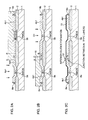
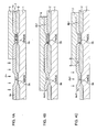
- Figs. 1A, 1B and 1C, and Figs. 2A, 2B and 2C are diagrammatic sectional views showing a manufacturing method of a semiconductor device according to the present embodiment in the order of its processes
- Fig. 3 is a diagrammatic plan view showing the semiconductor device manufactured by the processes shown in Figs. 1A, 1B and 1C and Figs. 2A, 2B and 2C in the process order seen from above.
- a field insulation film 2 is formed in an element separation region using a LOCOS method or the like.
- a gate insulation film 3a in an NMOS forming region, and a gate insulation film 3b in a PMOS forming region separated by the field insulation film 2 are formed.
- a polysilicon film 4 is laminated on the gate insulation films 3a and 3b, and the field insulation film 2 by a method such as pyrolysis of SiH 4 gas in a nitrogen gas atmosphere.
- an window for an n-type formation of a gate electrode is formed by covering a PMOS forming region 4b of the polysilicon film 4 with a first resist mask 5 as a first mask layer, and a phosphorus ion (P + ) as a first impurity is injected under the condition of, for instance, 20KeV, 4 ⁇ 10 15 cm -2 from above.
- the NMOS forming region 4a of the polysilicon gate film 4 is converted into an n-type in a concentration of about 2.5 ⁇ 10 20 cm -3 . Then, the first resist mask 5 is exfoliated and the exfoliated portion is washed.
- an n-type formation pattern data (a polysilicon n-type formation resist pattern in Fig. 3) to form the polysilicon film 4 into an n-type in covering the first resist mask 5 can be created by only shifting n-well data so that it is easily created automatically.
- a gate forming region of the polysilicon film 4 including the NMOS forming region 4a of the polysilicon gate film 4, and the PMOS forming region 4b of the polysilicon gate film 4 where no ion is doped is covered with a second resist mask 6, and the polysilicon film 4 is patterned using, for instance, photolithography and dry etching to form gate electrode forming layers 4a1 and 4b1. Then, the second resist mask 6 is exfoliated and washed.
- a non-doped region 4b1 and a partial region of an n-type forming region 4a1 are covered with a third resist mask 7 as a second mask layer so as to include a boundary portion between the region 4b1 where ions in the gate electrode forming layers 4a1 and 4b1 are not doped (hereinafter referred to a non-doped region) and an n-type formed region 4a1 (hereinafter referred to as an n-type forming region).
- an NMOSLDD ion implantation window to form an LDD in the NMOS forming region is arranged to position between an n-type formation window of the gate electrode (an end B of the first resist mask 5 on the NMOS forming region side) and the NMOS gate electrode (an end of the polysilicon film 4 positioned on the gate insulation film 3a on the PMOS forming region side).
- the distance between the n-type formation window of the gate electrode (the end B of the first resist mask) and the NMOSLDD forming ion implantation window (the end A of the third resist mask 7) is preferably about 0.3 ⁇ m in the case of, for instance, 0.25 ⁇ m device.
- an arsenic ion (As + ) as a second impurity is injected from above under the condition of, for instance, 10KeV, 3 ⁇ 10 14 cm -2 to perform ion implantation for LDD formation of an NMOS transistor.
- arsenic ion (As + ) for forming the LDD as above is because it is necessary to form a shallow junction in the semiconductor substrate 1.
- the use of the arsenic ion (As + ) gives the advantage of not only making the ion implantation energy low, but also making the element to be low resistant so that the drive capacity can be improved.
- An implantation window data for the LDD (the NMOSLDD resist pattern in Fig. 3) to form the above-described NMOSLDD ion implantation window can be automatically created by shifting the n-type formation pattern data (the polysilicon n-type formation resist pattern in Fig. 3) of the gate electrode.
- the third resist mask 7 is exfoliated and the exfoliated portion is washed.
- a non-doped region 4b1 and a partial region of the n-type forming region 4a1 are covered with a fourth resist mask 9 as a fourth mask layer so as to include a non-doped region 4b1 of the gate electrode forming layers 4a1 and 4b1, and a boundary portion between the non-doped region 4b1 and the n-type forming region 4a1.
- an end A of the fourth resist mask 9 on the NMOS forming region side is managed to position between an end of the n-type formation window of the gate electrode (an end B of the first resist mask 5 on the NMOS forming region side) and the NMOS gate electrode (an end of the polysilicon film 4 positioned on the gate insulation film 3a on the PMOS forming region side) in a similar manner to the case of NMOSLDD ion implantation described above.
- the distance between the n-type formation window of the gate electrode (the end B of the first resist mask 5) and the NMOS source and drain forming ion implantation window (the end A of the fourth resist mask 9) is preferably about 0.3 ⁇ m in the case of, for instance, 0.25 ⁇ m device.
- an arsenic ion (As + ) as a fourth impurity is injected from above under the condition of, for instance, 40KeV, 2 ⁇ 10 15 cm -2 .
- a source region and a drain region in high concentration are formed in the NMOS forming region of the semiconductor substrate.
- the reason of using the arsenic ion (As + ) to form the source region and the drain region is because the ion implantation energy required can be small, and the element can be made low resistant so that the drive capacity can be improved.
- the difference between the ion concentration N + in a region covered with the fourth resist mask 9 and the ion concentration N ++ in a region not covered with, in the n-type forming region 4a1 of the gate electrode forming layers 4a1 and 4b1 is about 1.5 ⁇ 10 20 cm -3 .
- the NMOS source and drain formation implantation window data (the NMOS source and drain resist pattern in Fig. 3) to form source and drain regions in the NMOS forming region is the same as the LDD implantation window data (the NMOSLDD resist pattern in Fig. 3) to form the NMOSLDD ion implantation window.
- the fourth resist mask 9 is exfoliated and the exfoliated portion is washed.
- an n-type forming region 4a1 excluding a region adjacent to the non-doped region 4b1 is covered with a fifth resist mask 10 as a third mask layer.
- an end C of the fifth resist mask 10 on the PMOS forming region is arranged to position between the n-type formation window (the end B of the first resist mask 5 on the NMOS forming region side) of the gate electrode and the NMOS gate electrode (an end of the polysilicon film 4 positioned on the gate insulation film 3a on the PMOS forming region side) in a similar manner to the case of NMOSLDD ion implantation described above.
- a boron ion (B + ) as a third impurity is injected from above under the condition of, for instance, 7KeV, 2 ⁇ 10 15 cm -2 .
- a non-doped region 4b1 is formed into a p-type (hereinafter referred to express the p-type non-doped region as a p-type forming region), and at the same time, a source region and a drain region in high concentration (PMOS LDD source and drain 14 in Fig. 3) are formed in the PMOS forming region of the semiconductor substrate.
- the implantation of the boron (B + ) is performed with an ion implantation amount less than the arsenic ion implantation amount (4 ⁇ 10 15 cm -2 ) for forming the NMOS forming region 4a shown in Fig. 1A. This is because the n-type forming region not covered with the fifth resist mask 10 is not to be converted into a p-type.
- the difference between the ion concentration N1 + in a region covered with the fifth resist mask 10 and the ion concentration N2 + in a region not covered with, in the region covered with the fourth resist mask 9 shown in Fig. 2A is about 1 ⁇ 10 20 cm -3 .
- the PMOS source and drain formation implantation window data (the PMOS source and drain resist pattern in Fig. 3) to form the source and drain regions in the above-described PMOS forming region can be automatically created by shifting the n-type pattern data of the above-described gate electrode (the polysilicon n-type formation resist pattern in Fig. 3), similar to the above-described LDD implantation window data.
- an ion-injected impurity is activated by heating an element forming region 1 of the semiconductor substrate.
- silicide 11 is formed in the gate electrode and the source and drain regions using a high melting point metal.
- a silicide non-forming region 12 where the above-described silicide 10 is not formed is formed in the vicinity of the central portion of n-type region 4a1 of the gate electrode forming layers 4a1 and 4b1.
- the silicide non-forming region 12 can be arranged not to overlap with a pn junction of the gate electrode forming layers 4a1 and 4b1, and a portion where the above-described silicide non-forming portion can be connected with polysilicon resistance in concentration of 1 ⁇ 10 20 cm -3 .
- the silicide non-forming region 12 is formed on the n-type forming region 4a1 of the gate electrode forming layers 4a1 and 4b1, so that the silicide non-forming region 12 does not overlap with the pn junction of the gate electrode forming layers 4a1 and 4b1,and the silicide film 11 is formed on the pn junction, a parasitic diode consisting of the pn junction is not formed on the gate electrode, which prevents the silicide non-forming region 12 from increasing in resistance.
- the semiconductor device of the present invention can be made finer than the semiconductor device in the prior dual structure.
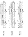
- Figs. 4A, 4B and 4C, and Figs. 5A, 5B and 5C are diagrammatic sectional views showing a manufacturing method of a semiconductor device according to the present embodiment in the order of its processes.
- Fig. 6 and Fig. 7 are diagrammatic plan views showing the semiconductor device manufactured by the processes shown in Figs. 4A, 4B and 4C and Figs. 5A, 5B and 5C in the process order seen from above.
- the method for manufacturing the semiconductor device of the present embodiment differs in a portion for forming a fifth resist mask 10 from the method for manufacturing the semiconductor device in the above-described first embodiment, the same portions as those in the first embodiment are given the same symbols and numerals and a detailed explanation thereof will be omitted.
- a field insulation film 2 is formed to separate a gate insulation film 3a of an NMOS forming region from a gate insulation film 3b of a PMOS forming region.
- a phosphorus ion (P + ) is injected under the condition of, for instance, 20KeV, 4 ⁇ 10 15 cm -2 from above to convert the NMOS forming region 4a of the polysilicon gate film 4 into an n-type. Then, the first resist mask 5 is exfoliated and the exfoliated portion is washed.
- an n-type formation pattern data (a polysilicon n-type formation resist pattern in Fig. 6) to convert the polysilicon film 4 into an n-type while covering the first resist mask 5 can be created only by shifting an n-well data and thus the automatic creation can be easily achieved.
- a gate forming region of the polysilicon film 4 is covered with a second resist mask 6, and the polysilicon film 4 is patterned to form the gate electrode forming layers 4a1 and 4b1. Then, the second resist mask 6 is exfoliated and washed.
- a non-doped region 4b1 and a partial region of the n-type forming region 4a1 are covered with a third resist mask 7 so as to include the non-doped region of the gate electrode forming layers 4a1 and 4b1, and a boundary portion between a non-doped region 4b1 and an n-type forming region 4a1.
- an NMOSLDD ion implantation window to form an LDD in the NMOS forming region is arranged to position between an n-type formation window of the gate electrode (an end B of the first resist mask 5 on the NMOS forming region side) and the NMOS gate electrode (an end of the polysilicon film 4 positioned on the gate insulation film 3a on the PMOS forming region side).
- an arsenic ion (As + ) is injected from above under the condition of, for instance, 10KeV, 3 ⁇ 10 14 cm -2 to perform ion implantation for the LDD of an NMOS transistor.
- the LDD implantation window data (the NMOSLDD resist pattern in Fig. 6) to form the above-described NMOSLDD ion implantation window can be automatically created by shifting the n-type pattern data of the gate electrode (the polysilicon n-type formation resist pattern in Fig. 6).
- the third resist mask 7 is exfoliated and the exfoliated portion is washed.
- a non-doped region 4b1 and a partial region of an n-type forming region 4a1 are covered with a fourth resist mask 9 as a fourth mask layer so as to include a boundary portion between the non-doped region 4b1 of the gate electrode forming layers 4a1 and 4b1 and the n-type formation region 4a1.
- an end A of a fourth resist mask 9 on the NMOS forming region side is managed to position between an end of the n-type formation window of the gate electrode (the end B of the first resist mask 5 on the NMOS forming region side) and the NMOS gate electrode (an end of the polysilicon film 4 positioned on the gate insulation film 3a on the PMOS forming region side) in a similar manner to the case of NMOSLDD ion implantation described above.
- an arsenic ion (As + ) as a fourth impurity is injected from above under the condition of, for instance, 40KeV, 2 ⁇ 10 15 cm -2 to form a source region and drain region in high concentration (an NMOS LDD S/D24 in Fig. 6 and Fig. 7) in the NMOS forming region of the semiconductor substrate.
- the difference between the ion concentration N + in a region covered with the fourth resist mask 9 and the ion concentration N ++ in a region not covered with, in the n-type region 4a1 of the gate electrode forming layers 4a1 and 4b1 is about 1.5 ⁇ 10 20 cm -3 .
- the NMOS source and drain formation implantation window data (the NMOS S/D resist pattern in Fig. 6) to form a source and drain regions in the NMOS forming region is the same as the LDD implantation window data (the NMOSLDD resist pattern in Fig. 6) to form the NMOSLDD ion implantation window.
- the fourth resist mask 9 is exfoliated and the exfoliated portion is washed.
- the non-doped region 4b1 excluding a region E to form the PMOS gate electrode and the n-type forming region 4a1 are covered with a sixth resist mask 21 as a third mask layer.
- an end D of the sixth resist mask 21 on the PMOS forming region side is arranged to position between an end B of the n-type formation window of the gate electrode and a PMOS gate electrode (an end of the polysilicon film 4 positioned on the gate insulation film 3b on the NMOS forming region side).
- the distance between the n-type formation window of the gate electrode (the end B of the first resist mask) and the PMOS source and drain ion implantation window (the end D of the sixth resist mask 21) is preferably about 0.3 ⁇ m in the case of, for instance, 0.25 ⁇ m device.
- a boron ion (B + ) as a third impurity is injected from above under the condition of, for instance, 7KeV, 2 ⁇ 10 15 cm -2 .
- a region E to form the PMOS gate electrode is converted into a p-type (hereinafter, a p-type formed non-doped region is expressed as a p-type forming region) and at the same time a source region and a drain region in high concentration (PMOS LDD source and drain 25 in Fig. 6 and Fig. 7) are formed in the PMOS forming region of the semiconductor substrate.
- the PMOS source and drain formation implantation window data (the PMOS source and drain resist pattern in Fig. 7) to form the source and drain regions in the above-described PMOS forming region can be automatically created by shifting the n-type formation pattern data of the gate electrode (the polysilicon n-type formation resist pattern in Fig. 7), similar to the above-described LDD implantation window data.
- an ion-injected impurity is activated by heating an element forming region 1 of the semiconductor substrate.
- silicide 22 is formed in the gate electrode, and the source and drain regions using a high melting point metal.
- a silicide non-forming region 23 where the silicide 22 is not formed is formed in the vicinity of the central portion of the n-type forming region 4a1 of the gate electrode forming layers 4a1 and 4b1.
- a silicide non-forming region 23 can be arranged not to overlap with a pn junction of the gate electrode forming layers 4a1 and 4b1, so that a portion where the above-described silicide is not formed can be connected with polysilicon resistance in concentration of 10 20 cm -3 .
- the silicide non-forming region 23 is formed on the n-type forming region 4a1 of the gate electrode forming layers 4a1 and 4b1, so that the silicide non-forming region 23 does not overlap with the pn junction of the gate electrode forming layers 4a1 and 4b1, and the silicide film 22 is formed on the pn junction, a parasitic diode consisting of the pn junction is not formed on the gate electrode, which prevents the silicide non-forming region 23 from increasing in resistance.
- the semiconductor device of the present embodiment can be made finer than the semiconductor device in the prior dual structure.
- the PMOS forming region can be converted into a p-type without a boron ion (B + ) being injected into the n-type forming region 4a.
- the method for manufacturing the semiconductor device according to the present embodiment as in the first embodiment, it has also an advantageous effect in such that the implantation concentration of the boron ion (B + ) is not required to be lower than the concentration of the arsenic ion (As + ) injected to form an n-type forming region 4a1.
- first impurity and the second impurity are not limited to these. Any substance will be acceptable provided that the mass of the element composing the first impurity is smaller than the mass of the element composing the second impurity.
- a third embodiment of the semiconductor device of the present invention and a manufacturing method thereof will be explained next.
- the first and second embodiments are the technology to remove unfavorable influences due to the silicide non-forming region accompanied by manufacturing of the NMOS transistor among the CMOS transistors in a dual gate structure.
- a technology to remove unfavorable influences due to the silicide non-forming region accompanied by manufacturing of the PMOS transistor will be explained.
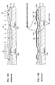
- Fig. 8A to Fig. 10B are diagrammatic sectional views showing a manufacturing method of a semiconductor device according to the present embodiment in the order of its processes.
- a field insulation film 32 is formed in an element separation region using a LOCOS method or the like.
- a gate insulation film 33a in an NMOS forming region, and a gate insulation film 33b in a PMOS forming region separated by the field insulation film 32 are formed.
- a polysilicon film 34 is laminated on the gate insulation films 33a and 33b, and the field insulation film 32 by a method such as pytolysis of SiH 4 gas in a nitrogen gas atmosphere.
- an n-type formation window of the gate electrode is formed by covering a PMOS forming region 34b of the polysilicon film 34 with a seventh resist mask 35 as a first mask layer, and a phosphorus ion (P + ) as a first impurity is injected under the condition of, for instance, 15KeV, 4 ⁇ 10 15 cm -2 from above.
- the NMOS forming region 34a of the polysilicon gate film 34 is converted into an n-type in a concentration of about 3.5 ⁇ 10 20 cm -3 . Then, the seventh resist mask 35 is exfoliated and the exfoliated portion is washed.
- an n-type formation pattern data to convert the polysilicon film 34 into an n-type by covering the seventh resist mask 35 can be created only by shifting n-well data so that it can be automatically created with ease.
- an NMOS forming region 34a of an n-type formed polysilicon film 34 is covered with an eighth resist mask 36 as a fifth mask layer, and a boron ion (B + ) as a fifth impurity is injected under the condition of, for instance, 5KeV, 4 ⁇ 10 15 cm -2 from above.
- the PMOS forming region 34b of the polysilicon film 34 is converted into a p-type in a concentration of about 3.5 ⁇ 10 20 cm -3 .
- the eighth resist mask 36 is exfoliated and the exfoliated portion is washed.
- a p-type formation pattern data to convert the polysilicon film 34 into a p-type by covering the eighth resist mask 36 can be created only by shifting p-well data so that it is automatically created with ease.
- a gate forming region of the polysilicon film 34 including the NMOS forming region 34a of the polysilicon gate film 34, and the PMOS forming region 34b of the polysilicon gate film 34 is covered with a ninth resist mask 37, and the polysilicon film 34 is patterned using, for instance, photolithography and dry etching to form a gate electrode forming layers 34a1 and 34b1. Then, the ninth resist mask 37 is exfoliated and washed.
- the p-type forming region 34b1 and a partial region of the n-type forming region 34a1 including a boundary region between 34a1 and 34b1 are covered with a tenth resist mask 38 as a second mask layer.
- an NMOSLDD ion implantation window to form an LDD in the NMOS forming region is arranged to position between an n-type formation window of the gate electrode (an end G of the seventh resist mask 35 on the NMOS forming region side) and the NMOS gate electrode (an end of the polysilicon film 34 positioned on the gate insulation film 33a on the PMOS forming region side).
- an arsenic ion (As + ) as a second impurity is injected from above under the condition of, for instance, 5KeV, 3 ⁇ 10 14 cm -2 to perform ion implantation for LDD of an NMOS transistor.
- arsenic ion (As + ) for forming the LDD as above is because it is necessary to form a shallow junction in the semiconductor substrate 1.
- the use of the arsenic ion (As + ) gives an advantage of not only making the ion implantation energy small, but also making the element to be low resistant so that the drive capacity can be improved.
- an implantation window data for the LDD to form the above-described NMOSLDD ion implantation window can be automatically created by shifting the n-type formation pattern data of the gate electrode.
- a PMOSLDD ion implantation window (an end I of the eleventh resist mask 39 of the NMOS forming region side) on the PMOS forming region side) is arranged to position between a p-type formation window of the gate electrode (an end G of the eighth resist mask 36 on the PMOS forming region side) and the PMOS gate electrode (an end of the polysilicon film 34 positioned on the gate insulation film 33b on the NMOS forming region side).
- an indium ion (In + ) as a sixth impurity is injected from above under the condition of, for instance, 5KeV, 3 ⁇ 10 14 cm -2 to perform ion implantation for LDD of the PMOS transistor.
- the reason to use the indium ion (In + ) for forming the LDD as above is because it is necessary to form a shallow junction in the semiconductor substrate 1.
- the use of the indium ion (In + ) gives an advantage of not only making the ion implantation energy low, but also making the element to be low resistant so that the drive capacity can be improved.
- the eleventh resist mask 39 is exfoliated and the exfoliated portion is washed.
- an arsenic ion (As + ) is injected from above under the condition of, for instance, 15KeV, 2 ⁇ 10 15 cm -2 to form a source region and a drain region in high concentration in the NMOS forming region of the semiconductor substrate (not shown).
- the reason of using an arsenic ion (As + ) to form the source region and the drain region as above is because the ion implantation energy required can be small, and the element can be made low resistant so that the drive capacity can be improved.
- the difference between the ion concentration N + in a region covered with the twelfth resist mask 41 and the ion concentration N ++ in a region not covered with, in the n-type forming region 34a1 of the gate electrode forming layers 34a1 and 34b1 is about 2 ⁇ 10 20 cm -3 .
- the NMOS source and drain formation implantation window data to form source and drain regions in the NMOS forming region is the same as the LDD implantation window data to form the above-described NMOSLDD ion implantation window.
- the difference between the ion concentration P + in a region covered with the thirteenth resist mask 42 and the ion concentration P ++ in a region not covered with, in the p-type forming region 34b1 of the gate electrode forming layers 34a1 and 34b1 is about 2 ⁇ 10 20 cm -3 .
- an ion-injected impurity is activated by heating an element forming region 31 of the semiconductor substrate.
- silicide 43 is formed in the gate electrode, and the source and drain regions using a high melting point metal.
- a silicide non-forming regions 44a to 44c where the silicide 43 is not formed is formed in the vicinity of the central portion of n-type forming region 34a1 or in the vicinity of the central portion of the p-type forming region 34b1 of the gate electrode forming layers 34a1 and 34b1.
- a silicide non-forming region 43 can be arranged not to overlap with a pn junction of the gate electrode forming layers 34a1 and 34b1, so that a portion where the silicide non-forming region 43 is formed can be connected with polysilicon resistance of 10 20 cm -3 in concentration.
- the silicide non-forming regions 44a to 44c do not overlap with a pn junction of the gate electrode forming regions 34a1 and 34b1, so that a silicide film 43 is formed on the pn junction, a parasitic diode consisting of the pn junction is not formed on the gate electrode in the PMOS transistor in a dual gate structure, which prevents resistance in the silicide non-forming region 44 from increasing.
- a phosphorus ion is used as a first impurity
- arsenic ions are used as second and fourth impurities
- the first impurity, and the second and fourth impurities are not limited to these. Any substance will be acceptable provided that the mass of the element composing the first impurity is smaller than the mass of the element composing the second and fourth impurities.
- Figs. 11A, 11B, and 11C and Figs. 12A, 12B, and 12C are diagrammatic sectional views showing a manufacturing method of a semiconductor device according to the present embodiment in the order of its processes.
- a PMOS forming region 54b of the polysilicon film 54 is covered with a fourteenth resist mask 55 as a first mask layer to form an n-type formation window of the gate electrode.
- a phosphorus ion (P + ) as a first impurity is injected under the condition of, for instance, 20KeV, 4 ⁇ 10 15 cm -2 from above to convert an NMOS forming region 54a of the polysilicon gate film 54 into an n-type. Then, the fourteenth resist mask 55 is exfoliated and the exfoliated portion is washed.
- an arsenic ion (As + ) as a second impurity is injected under the condition of, for instance, 10KeV, 3 ⁇ 10 14 cm -2 from above to perform ion implantation for an LDD of the NMOS transistor.
- the sixteenth resist mask 57 is exfoliated and the exfoliated portion is washed.
- an end L of the seventeenth resist mask 59 on the NMOS forming region side is arranged to position between an n-type formation window of the gate electrode (an end K of the fourteenth resist mask 55 on the NMOS forming region side) and an NMOS gate electrode (an end of the polysilicon film 54 positioned on the gate insulation film 53a on the PMOS forming region side) in a similar manner to the case of NMOSLDD ion implantation described above.
- an arsenic ion (As + ) as an fourth impurity is injected from above under the condition of, for instance, 40KeV, 2 ⁇ 10 15 cm -2 to form a source region and a drain region in high concentration in the NMOS forming region of the semiconductor substrate (not shown) .
- the difference between the ion concentration N + in a region covered with the seventeenth resist mask 59 and the ion concentration N ++ in a region not covered with, in the NMOS gate electrode forming layer 54a1 is about 1.5 ⁇ 10 20 cm -3 .
- a boron ion (B + ) as a third impurity is injected from above under the condition of, for instance, 7KeV, 2 ⁇ 10 15 cm -2 .
- a PMOS gate electrode forming layer 54b1 for forming the PMOS gate electrode is converted into a p-type, and at the same time, a source region and a drain region in high concentration are formed in the PMOS forming region of the semiconductor substrate (not shown).
- an ion-injected impurity is activated by heating an element forming region 51 of the semiconductor substrate.
- silicides 61a and 61b are formed in the gate electrode and the source and drain regions using a high melting point metal.
- a silicide non-forming region 62 where the silicide 61a is not formed is formed on the NMOS gate electrode forming layer 54a1.
- a silicide non-forming region 62 can be formed on an n-type forming region (NMOS gate electrode forming layer 54a1), similarly to the case of the CMOS transistor in the first to third embodiments of the present embodiment, and the silicide non-forming region 62 is not to position on the pn junction.
- the formation of a parasitic diode consisting of the pn junction on the gate electrode can be prevented, and resistance in the silicide non-forming region 62 can be prevented from increasing.
- the silicide 61b can be perfectly formed on the PMOS gate electrode forming layer 54b1. Accordingly, unfavorable influence on the operation of the semiconductor device due to the silicide formation can be completely eliminated.
- the conditions of the ion implantation for a phosphorus ion, a boron ion, and an arsenic ion are not limited to the values described in the first to fourth embodiments. That is, it is acceptable for a phosphorus ion to implant under the condition of 20keV, 4 ⁇ 10 15 cm -2 or less, for a boron ion under the condition of 7keV, 4 ⁇ 10 15 cm -2 or less, and for an arsenic ion under the condition of 10keV, 6 ⁇ 10 13 cm -2 or more.
- the same conductive-type semiconductor films formed above the semiconductor substrate are connected while having two or more differences in concentration along the surface of the semiconductor substrate, and a non-forming region of the silicide film can be formed on the region having the difference in concentration.
- This makes it possible to form the silicide non-forming region, formed on the semiconductor film on the same conductive-type semiconductor films, and a parasitic diode consisting of a pn junction is prevented from being formed on the gate electrode.
- cost reduction and fine structure formation can be realized while restraining unfavorable influence due to formation of silicide on the semiconductor film.
Landscapes
- Metal-Oxide And Bipolar Metal-Oxide Semiconductor Integrated Circuits (AREA)
- Electrodes Of Semiconductors (AREA)
- Insulated Gate Type Field-Effect Transistor (AREA)
- Internal Circuitry In Semiconductor Integrated Circuit Devices (AREA)
- Semiconductor Integrated Circuits (AREA)
Abstract
Description
As shown in Fig. 13A, after forming a
Claims (45)
- A semiconductor device, comprising:wherein at least one of the same conductive-type semiconductor films formed above said semiconductor substrate has two or more differences in concentration along a surface of said semiconductor substrate, being in electrical connection therebetween.a semiconductor film formed above a semiconductor substrate; anda silicide film formed on said semiconductor film,
- The semiconductor device according to claim 1, wherein a non-forming region of said silicide film is on said region having the difference in concentration.
- The semiconductor device according to claim 2, wherein the non-forming region of said silicide film is positioned on a boundary between the region having the highest concentration and the region having the next highest concentration.
- The semiconductor device according to any of the preceding claims, wherein an impurity existing in the region of high concentration on said semiconductor film is heavier in mass than an impurity existing in a region of low concentration in the semiconductor film.
- The semiconductor device according to any of the preceding claims, said semiconductor device comprising:wherein a region of low concentration in said first conductive-type semiconductor film is in electrical connection with said second conductive-type semiconductor film.a first conductive-type semiconductor film having two or more differences in concentration; anda second conductive-type semiconductor film different from said first conductive-type semiconductor,
- The semiconductor device according to claim 5, wherein the region of low concentration in said first conductive-type semiconductor film and said second conductive-type semiconductor film are in electrical connection with each other along the surface of said semiconductor substrate.
- The semiconductor device according to any of the preceding claims, said semiconductor device comprising:wherein said non-doped semiconductor film is connected while being sandwiched between the region of low concentration in said first conductive-type semiconductor film and said second conductive-type semiconductor film along the surface of said semiconductor substrate.a first conductive-type semiconductor film having two or more differences in concentration;a second conductive-type semiconductor film different from said first conductive-type semiconductor; anda non-doped semiconductor film in which an impurity is not doped,
- The semiconductor device according to any of claims 1 to 4, said semiconductor device comprising:wherein the region of low concentration in said first conductive-type semiconductor film and the region of low concentration in the second conductive-type semiconductor film are in electrical connection with each other.a first conductive-type semiconductor film having two or more differences in concentration; anda second conductive-type semiconductor film different from said first conductive-type semiconductor, and having two or more differences in concentration,
- The semiconductor device according to claim 8, wherein the region of low concentration in said first conductive-type semiconductor film and the region of low concentration in said second conductive-type semiconductor film are in electrical connection with each other along the surface of said semiconductor substrate.
- The semiconductor device according to claim 5 or any claim dependent thereon, wherein an arsenic ion exists in the region of high concentration in said first conductive-type semiconductor film.
- The semiconductor device according to claim 5 or any claim dependent thereon, wherein a phosphorus ion exists in the region of low concentration in said first conductive-type semiconductor film.
- The semiconductor device according to claim 8 or 9, wherein an indium ion exists in the region of high concentration in said second conductive-type semiconductor film.
- The semiconductor device according to claim 8, 9 or 12, wherein a boron ion exists in the region of low concentration in said second conductive-type semiconductor film.
- The semiconductor device according to any of the preceding claims,
wherein the semiconductor device comprises:wherein said semiconductor device includes a transistor in which said semiconductor film serves as a gate, said insulation film serves as a gate insulation film, and said diffusion layers serve as a source and a drain.an insulation film formed on the surface of said semiconductor substrate; anddiffusion layers formed in said semiconductor substrate to sandwich a lower region of the same conductive-type semiconductor film, and - The semiconductor device according to claim 14, wherein said semiconductor device includes a CMOS transistor,
wherein said CMOS transistor comprises:a first MOS transistor in which said first conductive-type semiconductor film serves as a gate, said insulation film serves as a gate insulation film, and said diffusion layers formed to sandwich the lower region of the first conductive-type semiconductor film serve as a source and a drain; anda second MOS transistor in which said second conductive-type semiconductor film serves as a gate, said insulation film serves as a gate insulation film, and said diffusion layers formed to sandwich the lower region of the second conductive-type semiconductor film serve as a source and a drain. - The semiconductor device according to claim 15, wherein the thickness of the insulation film formed on the boundary region between said first MOS transistor and said second MOS transistor is thicker than the thickness of other regions.
- The semiconductor device according to claim 14, 15 or 16, wherein said diffusion layers include difference in concentration.
- The semiconductor device according to any of claims 14 to 17, wherein side wall spacers are formed on both sides of said semiconductor film.
- A manufacturing method of a semiconductor device, comprising:a first step of forming a semiconductor film above a semiconductor substrate;a second step of forming a first mask layer covering a partial region of said semiconductor film;a third step of forming a first conductive-type semiconductor film in said semiconductor film by injecting a first impurity in a first conductive-type into said semiconductor film using said first mask layer as a mask;a fourth step of removing said first mask layer;a fifth step of forming a second mask layer covering a partial region of said first conductive-type semiconductor film and a semiconductor film different from said first conductive-type semiconductor film to include a boundary region between said first conductive-type semiconductor film and a semiconductor film different from said first conductive-type semiconductor film;a sixth step of forming the first conductive-type semiconductor film of high concentration and the first conductive-type semiconductor film of low concentration by injecting the second impurity of the same conductive type as said first conductive type, composing of a heavier element in mass than said first impurity, into said semiconductor film, using said second mask layer as a mask;a seventh step of removing said second mask layer; andan eighth step of forming silicide on said semiconductor film.
- The method for manufacturing the semiconductor device according to claim 19, further comprising the steps between said seventh step and eighth step:a ninth step of forming a third mask layer covering a partial region or a whole region of said first conductive-type semiconductor film of low concentration and said first conductive-type semiconductor film of high concentration;a tenth step of injecting a third impurity in a second conductive-type different from said first conductive-type into said semiconductor film using said third mask layer as a mask; andan eleventh step of removing said third mask layer.
- The method for manufacturing the semiconductor device according to claim 19 or 20, further comprising the steps between said seventh step and ninth step:a twelfth step of forming side wall spacers on both sides of said semiconductor film;a thirteenth step of forming a fourth mask layer covering a partial region of said first conductive-type semiconductor film and a semiconductor film different from said first conductive-type semiconductor film to include a boundary region between said first conductive-type semiconductor film and a semiconductor film different from said first conductive-type semiconductor film;a fourteenth step of injecting a fourth impurity in the same conductive-type as said first conductive-type, composing of an element heavier in mass than said first impurity into said semiconductor film using said fourth mask layer as a mask; anda fifteenth step of removing said fourth mask layer.
- The method for manufacturing the semiconductor device according to claim 19, 20 or 21, further comprising the steps between said fourth step and fifth step:a sixteenth step of forming said fifth mask layer covering said first conductive-type semiconductor film;a seventeenth step of converting a semiconductor film different from said first conductive-type semiconductor film into a second conductive-type semiconductor film by injecting a fifth impurity in the second conductive-type different from said first conductive-type semiconductor film into said semiconductor film using said fifth mask layer as a mask; andan eighteenth step of removing said fifth mask layer,and further comprising the steps between said seventh step and the twelfth step:a nineteenth step of forming a sixth mask layer covering said first conductive-type semiconductor film and a partial region of said second conductive-type semiconductor film to include a boundary region between said first conductive-type semiconductor film and said second conductive-type semiconductor film;a twentieth step of forming the second conductive-type semiconductor film of high concentration and the second conductive-type semiconductor film of low concentration by injecting a sixth impurity in the same conductive-type as said second conductive-type, composing of an element heavier in mass than said fifth impurity into said semiconductor film, using said sixth mask layer as a mask; anda twenty first step of removing said sixth mask.
- The method for manufacturing the semiconductor device according to any of claims 19 to 22, wherein said third step comprises implantation of a phosphorus ion into said semiconductor film.
- The method for manufacturing the semiconductor device according to claim 19 or any claim dependent thereon, wherein said sixth step comprises implantation of an arsenic ion into said semiconductor film.
- The method for manufacturing the semiconductor device according to claim 20 or any claim dependent thereon, wherein said ninth step is to form a third mask layer covering said first conductive-type semiconductor film and a partial region of a semiconductor film different from said first conductive-type semiconductor film to include a boundary region between said first conductive-type semiconductor film and a semiconductor film different from said first conductive-type semiconductor film.
- The method for manufacturing the semiconductor device according to claim 21 or any claim dependent thereon, wherein said tenth step comprises implantation of the second conductive-type impurity in lower concentration than the first conductive-type impurity which is injected into a semiconductor film in said third step.
- The method for manufacturing the semiconductor device according to claim 26, wherein said tenth step comprises implantation of a boron ion into said semiconductor film.
- The method for manufacturing the semiconductor device according to claim 21 or any claim dependent thereon, wherein said fourteenth step comprises implantation of the same impurity as said second impurity.
- The method for manufacturing the semiconductor device according to claim 28, wherein said fourteen step comprises implantation of an indium ion into said semiconductor film.
- The method for manufacturing the semiconductor device according to claim 22 or any claim dependent thereon, wherein said seventeenth step comprises implantation of a boron ion into said semiconductor film.
- The method for manufacturing the semiconductor device according to claim 22 or any claim dependent thereon, wherein said twentieth step comprises implantation of an indium ion into said semiconductor film.
- The method for manufacturing the semiconductor device according to claim 19 or any claim dependent thereon, further comprising a twenty second step of forming an insulation film on the surface of said semiconductor substrate before said first step,
wherein said first step comprises forming of a semiconductor film on the semiconductor substrate on which said insulation film is formed. - A semiconductor device, comprising:wherein said silicide film is formed at least on a junction of said gate semiconductor film, and at least one of the same conductive-type semiconductor films has two or more differences in concentration.a gate semiconductor film formed above a semiconductor substrate in a state that two different conductive-type semiconductor films are connected with each other; anda silicide film formed on said gate semiconductor film,
- The semiconductor device according to claim 33, wherein said silicide film non-forming region is formed on said region having difference in concentration.
- The semiconductor device according to claim 33 or 34, wherein an impurity existing in a region of high concentration in the same conductive type semiconductor film is heavier in mass than the impurity existing in a region of low concentration in said semiconductor film.
- The semiconductor device according to any of claims 33 to 35, wherein said difference in concentration is 1.5×1020 cm-3 or more and 2×1020 cm-3 or less.
- A manufacturing method of a semiconductor device, in manufacturing a semiconductor device by forming a silicide film on a gate semiconductor film after forming said gate semiconductor film in which two different conductive-type semiconductor films are in junction with each other, above a gate semiconductor substrate, said manufacturing method of the semiconductor device comprising:a first step of forming a region of low concentration in said same conductive-type semiconductor film by injecting a light element impurity ion into at least one of the same conductive-type semiconductor film out of said gate semiconductor films;a second step of forming a region of high concentration in said same conductive-type semiconductor film by injecting a heavy element impurity ion heavier in mass than said light element into the region side of low concentration in the same conductive-type semiconductor film with respect to the junction of said two different conductive-type semiconductor films; anda third step of forming silicide film at least on the junction of said two different conductive-type semiconductor films.
- The method for manufacturing the semiconductor device according to claim 37, wherein said first step comprises implantation of at least either one of a phosphorus ion or a boron ion.
- The method for manufacturing the semiconductor device according to claim 37 or 38, wherein said second step comprises implantation of at least either one of an arsenic ion or an indium ion.
- A semiconductor device comprising:a gate electrode forming layer (4a, 4b) having first, second and third doped portions extending continuously one after the next across a semiconductor substrate, said first and third doped portions being of opposite conductivity types (n, p) and said second doped region (A-B) being of the same conductivity type (n) as one of said first and third doped portions so that a pn junction is formed at a first boundary location (B) where said second doped portion meets said one doped portion.
- A device as claimed in claim 40, having a silicide film formed over said first, second and third doped portions.
- A device as claimed in claim 40 or 41, wherein said silicide film is formed over said first boundary location (B).
- A device as claimed in claim 1, 2 or 3, wherein said silicide film is not formed, or not formed properly, over a second boundary location (A) where said second doped portion meets the other of said first and third doped portions.
- A method of manufacturing a semiconductor device in which first, second, and third portions of a gate electrode forming layer extend continuously one after the next across a semiconductor substrate, the method comprising:effecting a first implantation into said gate electrode forming layer using a mask (9) to cover said first, second and third portions such that an exposed further portion of said layer, on the other side of said first portion from said second portion, is doped with ions of a first conductivity type and said first and second portions are also doped with such ions to a lesser extent;effecting a second ion implantation into said gate electrode forming layer using a mask (10) to cover said first and further portions such that the exposed second and third portions are doped with ions of a second conductivity type opposite to said first conductivity type and said first portion is also doped with such ions to a lesser extent whilst remaining of said first conductivity type.
- A method as claimed in claim 44, further comprising:forming a silicide film (11) on said gate electrode forming layer after said second ion implantation.
Applications Claiming Priority (2)
| Application Number | Priority Date | Filing Date | Title |
|---|---|---|---|
| JP2001377623A JP4000256B2 (en) | 2001-12-11 | 2001-12-11 | Semiconductor device and manufacturing method thereof |
| JP2001377623 | 2001-12-11 |
Publications (3)
| Publication Number | Publication Date |
|---|---|
| EP1320130A2 true EP1320130A2 (en) | 2003-06-18 |
| EP1320130A3 EP1320130A3 (en) | 2005-05-11 |
| EP1320130B1 EP1320130B1 (en) | 2007-06-20 |
Family
ID=19185541
Family Applications (1)
| Application Number | Title | Priority Date | Filing Date |
|---|---|---|---|
| EP02252913A Expired - Lifetime EP1320130B1 (en) | 2001-12-11 | 2002-04-25 | Semiconductor device and manufcaturing method thereof |
Country Status (7)
| Country | Link |
|---|---|
| US (1) | US6781207B2 (en) |
| EP (1) | EP1320130B1 (en) |
| JP (1) | JP4000256B2 (en) |
| KR (1) | KR100815379B1 (en) |
| CN (1) | CN100386878C (en) |
| DE (1) | DE60220762T2 (en) |
| TW (1) | TW577146B (en) |
Families Citing this family (21)
| Publication number | Priority date | Publication date | Assignee | Title |
|---|---|---|---|---|
| JP2004342821A (en) * | 2003-05-15 | 2004-12-02 | Renesas Technology Corp | Semiconductor device |
| US7197896B2 (en) | 2003-09-05 | 2007-04-03 | 3M Innovative Properties Company | Methods of making Al2O3-SiO2 ceramics |
| JP2005203436A (en) * | 2004-01-13 | 2005-07-28 | Seiko Epson Corp | Semiconductor device manufacturing method and semiconductor device |
| JP2005322730A (en) * | 2004-05-07 | 2005-11-17 | Renesas Technology Corp | Semiconductor device and manufacturing method thereof |
| JP4268569B2 (en) * | 2004-06-16 | 2009-05-27 | 富士通マイクロエレクトロニクス株式会社 | Manufacturing method of semiconductor device |
| KR100647882B1 (en) * | 2004-07-09 | 2006-11-24 | 주식회사 마루스 | Connector for electric connector with connection structure |
| JP4969779B2 (en) * | 2004-12-28 | 2012-07-04 | 株式会社東芝 | Manufacturing method of semiconductor device |
| JP2006202860A (en) * | 2005-01-19 | 2006-08-03 | Toshiba Corp | Semiconductor device and manufacturing method thereof |
| KR100811267B1 (en) * | 2005-12-22 | 2008-03-07 | 주식회사 하이닉스반도체 | Method of fabricating the dual gate in semiconductor device |
| JP5190189B2 (en) * | 2006-08-09 | 2013-04-24 | パナソニック株式会社 | Semiconductor device and manufacturing method thereof |
| CN101577286B (en) * | 2008-05-05 | 2012-01-11 | 联华电子股份有限公司 | Composite transfer gate and manufacturing method thereof |
| US11193634B2 (en) * | 2012-07-03 | 2021-12-07 | Tseng-Lu Chien | LED and/or laser light source or bulb for light device |
| JP5559567B2 (en) * | 2010-02-24 | 2014-07-23 | パナソニック株式会社 | Semiconductor device |
| JP5857225B2 (en) | 2011-03-25 | 2016-02-10 | パナソニックIpマネジメント株式会社 | Semiconductor device |
| FR2981503A1 (en) * | 2011-10-13 | 2013-04-19 | St Microelectronics Rousset | TRANSISTOR MOS NOT SUBJECT TO HUMP EFFECT |
| US9196624B2 (en) * | 2012-07-10 | 2015-11-24 | Cypress Semiconductor Corporation | Leakage reducing writeline charge protection circuit |
| CN105206528A (en) * | 2014-06-17 | 2015-12-30 | 北大方正集团有限公司 | Manufacturing method of planar VDMOS device |
| JP6382025B2 (en) * | 2014-08-22 | 2018-08-29 | ルネサスエレクトロニクス株式会社 | Semiconductor device and manufacturing method thereof |
| JP2015188103A (en) * | 2015-06-03 | 2015-10-29 | ラピスセミコンダクタ株式会社 | Manufacturing method of semiconductor device |
| US10446567B2 (en) * | 2017-03-31 | 2019-10-15 | Asahi Kasei Microdevices Corporation | Nonvolatile storage element and reference voltage generation circuit |
| US10734489B2 (en) * | 2018-07-31 | 2020-08-04 | Taiwan Semiconductor Manufacturing Co., Ltd. | Method for forming semiconductor device structure with metal silicide layer |
Family Cites Families (26)
| Publication number | Priority date | Publication date | Assignee | Title |
|---|---|---|---|---|
| JP2895166B2 (en) * | 1990-05-31 | 1999-05-24 | キヤノン株式会社 | Method for manufacturing semiconductor device |
| JPH06244369A (en) | 1993-02-19 | 1994-09-02 | Sony Corp | CMOS transistor, connection hole with gate electrode thereof, and method of manufacturing the same |
| JP3039200B2 (en) * | 1993-06-07 | 2000-05-08 | 日本電気株式会社 | MOS transistor and method of manufacturing the same |
| JPH0786421A (en) | 1993-09-13 | 1995-03-31 | Fujitsu Ltd | Complementary MOS transistor and manufacturing method thereof |
| JP3249292B2 (en) | 1994-04-28 | 2002-01-21 | 株式会社リコー | Complementary MIS semiconductor device with dual gate structure |
| JPH098040A (en) * | 1995-06-16 | 1997-01-10 | Sony Corp | Wiring and method of forming the same |
| JPH0974195A (en) * | 1995-07-06 | 1997-03-18 | Mitsubishi Electric Corp | Semiconductor device and method of manufacturing semiconductor device |
| JPH0927555A (en) * | 1995-07-10 | 1997-01-28 | Ricoh Co Ltd | Semiconductor device and manufacturing method thereof |
| JPH0992823A (en) * | 1995-09-26 | 1997-04-04 | Matsushita Electric Ind Co Ltd | Semiconductor device and manufacturing method thereof |
| JP3393249B2 (en) * | 1995-12-27 | 2003-04-07 | ソニー株式会社 | Semiconductor device having dual gate structure and method of manufacturing the same |
| JPH09205152A (en) * | 1996-01-25 | 1997-08-05 | Sony Corp | CMOS semiconductor device having two-layer gate electrode structure and manufacturing method thereof |
| TW322591B (en) * | 1996-02-09 | 1997-12-11 | Handotai Energy Kenkyusho Kk | |
| JPH09246541A (en) | 1996-03-07 | 1997-09-19 | Sony Corp | Method for manufacturing semiconductor device |
| EP0798785B1 (en) * | 1996-03-29 | 2003-12-03 | STMicroelectronics S.r.l. | High-voltage-resistant MOS transistor, and corresponding manufacturing process |
| JP2910839B2 (en) | 1996-06-25 | 1999-06-23 | 日本電気株式会社 | Semiconductor device and manufacturing method thereof |
| JP4142753B2 (en) * | 1996-12-26 | 2008-09-03 | 株式会社東芝 | Sputtering target, sputtering apparatus, semiconductor device and manufacturing method thereof |
| EP0923116A1 (en) * | 1997-12-12 | 1999-06-16 | STMicroelectronics S.r.l. | Process for manufacturing integrated multi-crystal silicon resistors in MOS technology and integrated MOS device comprising multi-crystal silicon resistors |
| KR100255134B1 (en) * | 1997-12-31 | 2000-05-01 | 윤종용 | Semiconductor device and method for manufacturing the same |
| JP3737914B2 (en) | 1999-09-02 | 2006-01-25 | 松下電器産業株式会社 | Semiconductor device and manufacturing method thereof |
| US6191460B1 (en) * | 1999-09-07 | 2001-02-20 | Integrated Device Technology, Inc. | Identical gate conductivity type static random access memory cell |
| JP2001156290A (en) * | 1999-11-30 | 2001-06-08 | Nec Corp | Semiconductor device |
| KR20010066122A (en) * | 1999-12-31 | 2001-07-11 | 박종섭 | Method for forming polycide dual gate of semiconductor device |
| JP2001210725A (en) | 2000-01-25 | 2001-08-03 | Matsushita Electric Ind Co Ltd | Semiconductor device |
| JP2001332630A (en) * | 2000-05-19 | 2001-11-30 | Sharp Corp | Method for manufacturing semiconductor device |
| JP2002217310A (en) * | 2001-01-18 | 2002-08-02 | Mitsubishi Electric Corp | Semiconductor device and method of manufacturing the same |
| US6894356B2 (en) * | 2002-03-15 | 2005-05-17 | Integrated Device Technology, Inc. | SRAM system having very lightly doped SRAM load transistors for improving SRAM cell stability and method for making the same |
-
2001
- 2001-12-11 JP JP2001377623A patent/JP4000256B2/en not_active Expired - Fee Related
-
2002
- 2002-03-21 US US10/101,974 patent/US6781207B2/en not_active Expired - Lifetime
- 2002-03-22 TW TW091105611A patent/TW577146B/en not_active IP Right Cessation
- 2002-04-18 KR KR1020020021255A patent/KR100815379B1/en not_active Expired - Fee Related
- 2002-04-25 DE DE60220762T patent/DE60220762T2/en not_active Expired - Lifetime
- 2002-04-25 EP EP02252913A patent/EP1320130B1/en not_active Expired - Lifetime
- 2002-05-16 CN CNB02119775XA patent/CN100386878C/en not_active Expired - Fee Related
Also Published As
| Publication number | Publication date |
|---|---|
| CN1426110A (en) | 2003-06-25 |
| CN100386878C (en) | 2008-05-07 |
| EP1320130A3 (en) | 2005-05-11 |
| US20030107090A1 (en) | 2003-06-12 |
| EP1320130B1 (en) | 2007-06-20 |
| DE60220762D1 (en) | 2007-08-02 |
| US6781207B2 (en) | 2004-08-24 |
| DE60220762T2 (en) | 2007-10-11 |
| JP2003179056A (en) | 2003-06-27 |
| KR100815379B1 (en) | 2008-03-20 |
| JP4000256B2 (en) | 2007-10-31 |
| KR20030047660A (en) | 2003-06-18 |
| TW577146B (en) | 2004-02-21 |
Similar Documents
| Publication | Publication Date | Title |
|---|---|---|
| EP1320130B1 (en) | Semiconductor device and manufcaturing method thereof | |
| CN100394614C (en) | Semiconductor device and method of forming the same | |
| US7663187B2 (en) | Semiconductor device and method of fabricating the same | |
| US7326997B2 (en) | Method and structure for enhancing both nMOSFET and pMOSFET performance with a stressed film | |
| US7534671B2 (en) | Method for integrally forming an electrical fuse device and a MOS transistor | |
| US9620423B2 (en) | Integrated circuit having chemically modified spacer surface | |
| JP2719351B2 (en) | Method of forming NPN bipolar transistor | |
| US7939896B2 (en) | SOI substrate contact with extended silicide area | |
| US7847401B2 (en) | Methods, systems and structures for forming semiconductor structures incorporating high-temperature processing steps | |
| US20070166969A1 (en) | Semiconductor device and method for manufacturing the same | |
| JP2002076136A (en) | Method for manufacturing semiconductor device | |
| US20140021552A1 (en) | Strain Adjustment in the Formation of MOS Devices | |
| US7618857B2 (en) | Method of reducing detrimental STI-induced stress in MOSFET channels | |
| JP5205779B2 (en) | Semiconductor device manufacturing method and semiconductor device | |
| US6958279B2 (en) | Method for manufacturing semiconductor device | |
| US7271414B2 (en) | Semiconductor device and method for fabricating the same | |
| JP2005236105A (en) | Semiconductor device and manufacturing method thereof | |
| US7253039B2 (en) | Method of manufacturing CMOS transistor by using SOI substrate | |
| JP3003747B2 (en) | Semiconductor device and manufacturing method thereof | |
| US20080145990A1 (en) | Method and structure for fabricating mos devices with a salicided gate and source/drain combined with a non-silicide source drain regions | |
| JP4921925B2 (en) | Manufacturing method of semiconductor device | |
| JPH09260590A (en) | Semiconductor device and manufacture thereof | |
| JP2973984B2 (en) | Method for manufacturing semiconductor device | |
| US20090093092A1 (en) | Soi substrate contact with extended silicide area |
Legal Events
| Date | Code | Title | Description |
|---|---|---|---|
| PUAI | Public reference made under article 153(3) epc to a published international application that has entered the european phase |
Free format text: ORIGINAL CODE: 0009012 |
|
| AK | Designated contracting states |
Designated state(s): AT BE CH CY DE DK ES FI FR GB GR IE IT LI LU MC NL PT SE TR |
|
| AX | Request for extension of the european patent |
Extension state: AL LT LV MK RO SI |
|
| PUAL | Search report despatched |
Free format text: ORIGINAL CODE: 0009013 |
|
| AK | Designated contracting states |
Kind code of ref document: A3 Designated state(s): AT BE CH CY DE DK ES FI FR GB GR IE IT LI LU MC NL PT SE TR |
|
| AX | Request for extension of the european patent |
Extension state: AL LT LV MK RO SI |
|
| RIC1 | Information provided on ipc code assigned before grant |
Ipc: 7H 01L 29/49 B Ipc: 7H 01L 21/8238 A |
|
| 17P | Request for examination filed |
Effective date: 20051107 |
|
| AKX | Designation fees paid |
Designated state(s): DE FR GB |
|
| RBV | Designated contracting states (corrected) |
Designated state(s): DE FR GB IT |
|
| GRAP | Despatch of communication of intention to grant a patent |
Free format text: ORIGINAL CODE: EPIDOSNIGR1 |
|
| GRAS | Grant fee paid |
Free format text: ORIGINAL CODE: EPIDOSNIGR3 |
|
| GRAA | (expected) grant |
Free format text: ORIGINAL CODE: 0009210 |
|
| AK | Designated contracting states |
Kind code of ref document: B1 Designated state(s): DE FR GB IT |
|
| REG | Reference to a national code |
Ref country code: GB Ref legal event code: FG4D |
|
| REF | Corresponds to: |
Ref document number: 60220762 Country of ref document: DE Date of ref document: 20070802 Kind code of ref document: P |
|
| EN | Fr: translation not filed | ||
| PLBE | No opposition filed within time limit |
Free format text: ORIGINAL CODE: 0009261 |
|
| STAA | Information on the status of an ep patent application or granted ep patent |
Free format text: STATUS: NO OPPOSITION FILED WITHIN TIME LIMIT |
|
| 26N | No opposition filed |
Effective date: 20080325 |
|
| PG25 | Lapsed in a contracting state [announced via postgrant information from national office to epo] |
Ref country code: FR Free format text: LAPSE BECAUSE OF FAILURE TO SUBMIT A TRANSLATION OF THE DESCRIPTION OR TO PAY THE FEE WITHIN THE PRESCRIBED TIME-LIMIT Effective date: 20080222 |
|
| GBPC | Gb: european patent ceased through non-payment of renewal fee |
Effective date: 20080425 |
|
| PG25 | Lapsed in a contracting state [announced via postgrant information from national office to epo] |
Ref country code: GB Free format text: LAPSE BECAUSE OF NON-PAYMENT OF DUE FEES Effective date: 20080425 |
|
| PGFP | Annual fee paid to national office [announced via postgrant information from national office to epo] |
Ref country code: IT Payment date: 20090424 Year of fee payment: 8 |
|
| PG25 | Lapsed in a contracting state [announced via postgrant information from national office to epo] |
Ref country code: IT Free format text: LAPSE BECAUSE OF NON-PAYMENT OF DUE FEES Effective date: 20100425 |
|
| PGFP | Annual fee paid to national office [announced via postgrant information from national office to epo] |
Ref country code: DE Payment date: 20190410 Year of fee payment: 18 |
|
| REG | Reference to a national code |
Ref country code: DE Ref legal event code: R119 Ref document number: 60220762 Country of ref document: DE |
|
| PG25 | Lapsed in a contracting state [announced via postgrant information from national office to epo] |
Ref country code: DE Free format text: LAPSE BECAUSE OF NON-PAYMENT OF DUE FEES Effective date: 20201103 |