EP1320109A1 - Multi-layered inductance element - Google Patents
Multi-layered inductance element Download PDFInfo
- Publication number
- EP1320109A1 EP1320109A1 EP02017813A EP02017813A EP1320109A1 EP 1320109 A1 EP1320109 A1 EP 1320109A1 EP 02017813 A EP02017813 A EP 02017813A EP 02017813 A EP02017813 A EP 02017813A EP 1320109 A1 EP1320109 A1 EP 1320109A1
- Authority
- EP
- European Patent Office
- Prior art keywords
- conductor line
- line segments
- conductor
- line
- inductance
- Prior art date
- Legal status (The legal status is an assumption and is not a legal conclusion. Google has not performed a legal analysis and makes no representation as to the accuracy of the status listed.)
- Withdrawn
Links
Images



Classifications
-
- H—ELECTRICITY
- H03—ELECTRONIC CIRCUITRY
- H03H—IMPEDANCE NETWORKS, e.g. RESONANT CIRCUITS; RESONATORS
- H03H7/00—Multiple-port networks comprising only passive electrical elements as network components
- H03H7/48—Networks for connecting several sources or loads, working on the same frequency or frequency band, to a common load or source
-
- H—ELECTRICITY
- H05—ELECTRIC TECHNIQUES NOT OTHERWISE PROVIDED FOR
- H05K—PRINTED CIRCUITS; CASINGS OR CONSTRUCTIONAL DETAILS OF ELECTRIC APPARATUS; MANUFACTURE OF ASSEMBLAGES OF ELECTRICAL COMPONENTS
- H05K1/00—Printed circuits
- H05K1/16—Printed circuits incorporating printed electric components, e.g. printed resistors, capacitors or inductors
- H05K1/165—Printed circuits incorporating printed electric components, e.g. printed resistors, capacitors or inductors incorporating printed inductors
-
- H—ELECTRICITY
- H01—ELECTRIC ELEMENTS
- H01F—MAGNETS; INDUCTANCES; TRANSFORMERS; SELECTION OF MATERIALS FOR THEIR MAGNETIC PROPERTIES
- H01F17/00—Fixed inductances of the signal type
- H01F17/0006—Printed inductances
- H01F17/0013—Printed inductances with stacked layers
-
- H—ELECTRICITY
- H01—ELECTRIC ELEMENTS
- H01F—MAGNETS; INDUCTANCES; TRANSFORMERS; SELECTION OF MATERIALS FOR THEIR MAGNETIC PROPERTIES
- H01F41/00—Apparatus or processes specially adapted for manufacturing or assembling magnets, inductances or transformers; Apparatus or processes specially adapted for manufacturing materials characterised by their magnetic properties
- H01F41/02—Apparatus or processes specially adapted for manufacturing or assembling magnets, inductances or transformers; Apparatus or processes specially adapted for manufacturing materials characterised by their magnetic properties for manufacturing cores, coils, or magnets
- H01F41/04—Apparatus or processes specially adapted for manufacturing or assembling magnets, inductances or transformers; Apparatus or processes specially adapted for manufacturing materials characterised by their magnetic properties for manufacturing cores, coils, or magnets for manufacturing coils
- H01F41/041—Printed circuit coils
- H01F41/045—Trimming
-
- H—ELECTRICITY
- H05—ELECTRIC TECHNIQUES NOT OTHERWISE PROVIDED FOR
- H05K—PRINTED CIRCUITS; CASINGS OR CONSTRUCTIONAL DETAILS OF ELECTRIC APPARATUS; MANUFACTURE OF ASSEMBLAGES OF ELECTRICAL COMPONENTS
- H05K2201/00—Indexing scheme relating to printed circuits covered by H05K1/00
- H05K2201/07—Electric details
- H05K2201/0707—Shielding
- H05K2201/0715—Shielding provided by an outer layer of PCB
-
- H—ELECTRICITY
- H05—ELECTRIC TECHNIQUES NOT OTHERWISE PROVIDED FOR
- H05K—PRINTED CIRCUITS; CASINGS OR CONSTRUCTIONAL DETAILS OF ELECTRIC APPARATUS; MANUFACTURE OF ASSEMBLAGES OF ELECTRICAL COMPONENTS
- H05K2201/00—Indexing scheme relating to printed circuits covered by H05K1/00
- H05K2201/09—Shape and layout
- H05K2201/09209—Shape and layout details of conductors
- H05K2201/095—Conductive through-holes or vias
- H05K2201/09536—Buried plated through-holes, i.e. plated through-holes formed in a core before lamination
-
- H—ELECTRICITY
- H05—ELECTRIC TECHNIQUES NOT OTHERWISE PROVIDED FOR
- H05K—PRINTED CIRCUITS; CASINGS OR CONSTRUCTIONAL DETAILS OF ELECTRIC APPARATUS; MANUFACTURE OF ASSEMBLAGES OF ELECTRICAL COMPONENTS
- H05K2201/00—Indexing scheme relating to printed circuits covered by H05K1/00
- H05K2201/09—Shape and layout
- H05K2201/09209—Shape and layout details of conductors
- H05K2201/09654—Shape and layout details of conductors covering at least two types of conductors provided for in H05K2201/09218 - H05K2201/095
- H05K2201/097—Alternating conductors, e.g. alternating different shaped pads, twisted pairs; Alternating components
Definitions
- the present invention relates to a multi-layered inductance element.
- Layered inductance elements have been utilized in radio frequency circuits or other electric circuits.
- a conventional multi-layered inductance element includes a plurality of layered dielectric substrates and looped conductor lines interposed therebetween.
- the looped conductor lines are interconnected via through-holes, thereby exhibiting a spiral configuration as a whole.
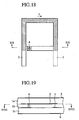
- Figs. 18 and 19 illustrate an example of conventional multi-layered inductance elements.
- the multi-layered inductance element includes a plurality of dielectric substrates 1a, 1b, and 1c, conductor lines 2 and 3 interposed therebetween, a through-hole 4, and a pair of ground conducting layers 5 and 6.
- the upper ground conducting layer 5 is provided on the top surface of the uppermost dielectric substrate 1a among the multi-layered dielectric substrates 1a, 1b, and 1c while the lower ground conducting layer 6 is disposed on the bottom surface of the lowermost dielectric substrates 1c.
- the upper conductor line 2 is interposed between the dielectric substrates 1a and 1b while the lower conductor line 3 is interposed between the dielectric substrates 1b and 1c.
- the through-hole 4 is formed in the intermediate dielectric substrate 1b, resulting in that the upper and lower conductor lines 2 and 3 are electrically connected with each other via conducting materials inside the through-hole 4.
- each of the conductor lines 2 and 3 has a looped shape although it is not closed completely.
- the hatched parts in Fig. 18 depict parts of the conductor lines 2 and 3 overlapping with or superimposed over each other. Since one end of the conductor line 2 is connected with one end of the conductor line 3 via the through-hole 4, conductor lines 2 and 3 cooperate to form a continuous spiral conductor line, which is analogous to a coil, having an inductance.
- a direct current is applied to the spiral conductor line, the direction of the current flow in the conductor line 2 is the same as that in the conductor line 3; for example, it is the clockwise direction as indicated by arrow I in Fig. 18.
- the direction of the current flow at each moment in the conductor line 2 is the same as that in the conductor line 3.
- the upper and lower conductor lines 2 and 3 should extend over and coincide perfectly with each other when viewed along the vertical direction (direction of thickness) of the multi-layered inductance element. It has been also considered that the vertical distance between the conductor lines 2 and 3 is preferably small. The reason is that such a preferable structure will strengthen the coupling of electromagnetic fields around the conductor lines 2 and 3, whereby the multi-layered inductance element can have a great inductance although its dimensions may be small.
- each of the conductor lines 2 and 3 is formed continuously so that the loop on the same plane is as long as possible.
- the sole through-hole 4 is utilized for connecting the upper and lower conductor lines 2 and 3 comprising the single spiral conductor line.
- the conventional multi-layered inductance element structured as described above has drawbacks that it is difficult to restrain the difference between the designed target inductance and the resulting inductance affected by an error in dimensions by manufacturing. It is also very difficult to adjust or tune the difference.
- the correlation between the positions of the conductor lines 2 and 3 is an important factor in quality. For example, when at least one of the conductor lines 2 and 3 is out of position so that the conductor lines 2 and 3 does not coincide with each other, the coupling of electromagnetic fields around the conductor lines 2 and 3 is degraded, resulting in decrease of the inductance.
- the thickness of the dielectric substrate 1b and hence the distance between the conductor lines 2 and 3 is small, the coupling of electromagnetic fields around the conductor lines 2 and 3 is strengthened, resulting in increase of the inductance. On the contrary, if the thickness of the dielectric substrate 1b is large, the inductance is decreased.
- dimensional errors such as positional errors of the conductor lines 2 and 3 and an error in thickness of the dielectric substrate 1b, lead variations of inductance in products of multi-layered inductance element.
- a multi-layered inductance element includes at least one dielectric substrate having a first and second surfaces, a first conductor line pattern, a second conductor line pattern, and a plurality of through-holes penetrating through the dielectric substrate.
- the first conductor line pattern includes a plurality of first conductor line segments being apart from each other and disposed on the first surface of the dielectric substrate, wherein the first conductor line segments exhibit a substantially looped configuration as a whole if adjacent first conductor line segments are connected with each other.
- the second conductor line pattern includes a plurality of second conductor line segments being apart from each other and disposed on the second surface of the dielectric substrate, wherein the second conductor line segments exhibit a substantially looped configuration as a whole if adjacent second conductor line segments are connected with each other.
- Each through-hole electrically connects one end of one of the first conductor line segments and one end of one of the second conductor line segments.
- Each of the first conductor line segments extends over at least a part of one of the second conductor line segments.
- the plurality of first conductor line segments and the plurality of second conductor line segments are connected by the through-holes, thereby forming a spiral conductor line in which a direction of current flow in the first conductor line pattern is the same as that in the second conductor line pattern.
- Each of the second conductor line segments includes a pair of end parts and a halfway part having a width which is smaller than that of the end parts. The end parts are connected to adjacent first conductor line segments via the through-holes.
- the halfway part with a smaller width of each second conductor line element tends to cancel an inductance decrement when the conductor line patterns are dislocated in relation to each other.
- the plurality of through-holes contributes to cancel an inductance variation when the thickness of the dielectric substrate varies. Therefore, the structure can restrain variations of inductance caused by errors in dimensions by manufacturing multi-layered inductance elements.
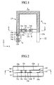
- Fig. 1 is a top cross-sectional view of a multi-layered inductance element according to a first embodiment of the present invention, showing conductor line patterns of the multi-layered inductance element.
- Fig. 2 is a side cross-sectional view of the multi-layered inductance element. More exactly, Fig. 1 is a cross-sectional view taken along line I-I in Fig. 2 while Fig. 2 is a cross-sectional view taken along line II-II in Fig. 1.
- the multi-layered inductance element includes dielectric substrates 1a, 1b, and 1c, a first conductor line pattern 12, a second conductor line pattern 13, and ground conducting layers 5 and 6.
- the first conductor line pattern 12 includes a plurality of first line segments 12a through 12c while the second conductor line pattern 13 includes a plurality of second line segments 13a through 13c connected to the first line segments 12a through 12c via through-holes 14a through 14e.
- the upper ground conducting layer 5 is provided on the top surface of the uppermost dielectric substrate 1a among the multi-layered dielectric substrates 1a, 1b, and 1c while the lower ground conducting layer 6 is disposed on the bottom surface of the lowermost dielectric substrates 1c.
- the first conductor line pattern 12 is interposed between the dielectric substrates 1a and 1b while the second conductor line pattern 13 is interposed between the dielectric substrates 1b and 1c.
- the through-holes 14a through 14e are formed to penetrate the dielectric substrate 1b, resulting in that the conductor line patterns 12 and 13 on the upper and lower surfaces of the dielectric substrate 1b are electrically connected with each other via conducting materials inside the through-holes 14a through 14e.
- each of the conductor line patterns 12 and 13 has a looped shape although it is not closed completely.
- the hatched parts in Fig. 1 depict parts of the conductor line patterns 12 and 13 overlapping with or superimposed over each other.
- the second conductor line pattern 13 and first conductor line pattern 12 will be described in more detail with reference to Figs. 3 and 4.
- the second conductor line pattern 13 includes a plurality of (for example, three) second line segments 13a through 13c being apart from one another.
- the second conductor line pattern 13 has two gaps where adjacent first conductor line segments are spaced apart. All of the second line segments 13a through 13c are located on a surface of the dielectric substrate 1b.
- the longest second line segment 13a includes four straight parts having a uniform width.
- the upper ends of two straight parts extending in parallel along the ordinate direction in Fig. 3 are connected at right angles with each end of the upper straight part extending along the abscissa direction.
- the lower end of the left straight part extending along the ordinate direction in Fig. 3 is connected at a right angle with an end of the lower shortest straight part extending along the abscissa direction.
- the lower shortest straight part extending along the abscissa direction is directed toward the right longest straight part extending along the ordinate direction. Accordingly, the second line segment 13a itself exhibits a looped configuration although it is not closed completely.
- Another second line segment 13b is aligned in the extending direction of the left straight part of the second line segment 13a. Although the second line segment 13b extends straightly, only both end parts thereof have the same width as that of the second line segment 13a while the halfway part thereof is coarctate.
- a further second line segment 13c is aligned in the extending direction of the lower straight part of the second line segment 13a. Accordingly, the short second line segment 13c is angled at 90 degrees with the short second line segment 13b. Although the second line segment 13c extends straightly, only both end parts thereof have the same width as that of the second line segment 13a while the halfway part thereof is coarctate. As illustrated, the second line segments 13b and 13c have the same dimensions and the same shape. However, the dimensions and/or shapes of the second line segments 13b and 13c may vary from each other.
- the second conductor line pattern 13 exhibits a substantially looped configuration as a whole if the adjacent second line segments 13a and 13c are interconnected and the adjacent second line segments 13a and 13b are also interconnected.
- the first conductor line pattern 12 includes a plurality of (for example, three) first line segments 12a through 12c being apart from one another.
- the first conductor line pattern 12 has two gaps where adjacent second conductor line segments are spaced apart. All of the first line segments 12a through 12c are located on a surface of the dielectric substrate 1b, which is opposite to the surface on which the second line segments 13a through 13c are located.
- the longest first line segment 12a includes four straight parts having a uniform width.
- the upper ends of two straight parts extending in parallel along the ordinate direction in Fig. 4 are connected at right angles with each end of the upper straight part extending along the abscissa direction.
- the lower end of the right straight part extending along the ordinate direction in Fig. 4 is connected at a right angle with an end of the lower shortest straight part extending along the abscissa direction.
- the lower shortest straight part extending along the abscissa direction is directed toward the left longest straight part extending along the ordinate direction. Accordingly, the first line segment 12a itself exhibits a looped configuration although it is not closed completely.
- a shorter first line segment 12b is aligned in the extending direction of the left straight part of the first line segment 12a.
- the first line segment 12b extends straightly and has a uniform width that is the same as that of the first line segment 12a.
- Another shorter first line segment 12c is aligned in the extending direction of the lower straight part of the first line segment 12a. Accordingly, the first line segment 12c is angled at 90 degrees with the first line segment 12b. The first line segment 12c extends straightly and has a uniform width that is the same as that of the first line segment 12a.
- the first conductor line pattern 12 also exhibits a looped configuration as a whole if the adjacent first line segments 12a and 12c are interconnected and the adjacent first line segments 12a and 12b are also interconnected.
- the hatched parts in Fig. 1 depict parts of the conductor line patterns 12 and 13 overlapping with or superimposed over each other.
- Each of the first line segments 12a through 12c extends over at least a part of one of the second line segments 13a through 13c.
- end parts of the first and second line segments are placed over each other, and the overlapping end parts are electrically interconnected via any of the through-holes 14a through 14e.
- first line segment 12b at the bottom left-hand corner in Fig. 1 extends over one end part of the second line segment 13b, and the overlapping parts are interconnected via the through-hole 14c.
- the other end part of the second line segment 13b extends over one end part of the first line segment 12a, and the overlapping parts are interconnected via the through-hole 14b.
- the other end part of the first line segment 12a extends over an end part of the second line segment 13c, and the overlapping parts are interconnected via the through-hole 14d.
- the other end part of the second line segment 13c extends over an end part of the first line segment 12c, and the overlapping parts are interconnected via the through-hole 14e.
- the other end part of the first line segment 12c extends over an end part of the second line segment 13a, and the overlapping parts are interconnected via the through-holes 14a. Most of the second line segment 13a extends over most of the first line segment 12a. In connection with the overlapping parts, it is preferable that the side edges of both line segments 12a and 13a coincide perfectly with each other.
- the line segments 12b, 13b, 12a, 13c, 12c, and 13a cooperate to form a single continuous spiral conductor line, which is analogous to a coil, having an inductance.
- a direct current is applied to the spiral conductor line
- the direction of the current flow in the first conductor line pattern 12 is the same as that in the second conductor line pattern 13; for example, it is the clockwise direction as indicated by arrow I in Fig. 1.
- the direction of the current flow at each moment in the first conductor line pattern 12 is the same as that in the second conductor line pattern 13.
- the first conductor line pattern 12 contains two gaps where adjacent first conductor line segments are spaced apart. More specifically, there are the gaps in parts A and B enclosed by dashed lines in Fig. 1: one is interposed between the first line segments 12b and 12a while the other gap is interposed between the first line segments 12c and 12a.
- the second line segment 13b extending over the gap in part A for connecting the adjacent first line segments 12b and 12a is angled at 90 degrees with the second line segment 13c extending over the gap in part B for connecting the adjacent first conductor line segments 12c and 12a.
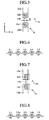
- Fig. 5 is an enlarged view of part A in Fig. 1.
- the first line segment 12a is connected with the first line segment 12b via the through-hole 14b, the wider end part of the second line segment 13b, the coarctate halfway part of the second line segment 13b having a width W, the other wider end part of the second line segment 13b, and the through-hole 14c.
- Fig. 5 shows the second line segment 13b formed at an ideal location in relation to the first line segments 12a and 12b. That is to say, both side edges of the wider end parts of the second line segment 13b coincide perfectly with the side edges of the first line segments 12a and 12b without any dislocation with respect to the abscissa direction (X direction). With respect to the ordinate direction (Y direction), the boundary between each end part and the coarctate halfway part of the second line segment 13b coincide perfectly with the end edge of the first line segment 12a or 12b without any dislocation.
- Fig. 6 is a schematic diagram showing a circuit equivalent to the structure shown in Fig. 5.
- L1 and L2 indicate the inductance values of the through-holes 14b and 14c, respectively.
- L5 indicates the inductance of the halfway part of the second line segment 13b having a smaller width W.
- L3 and L4 indicate the inductance values of both end parts of the second line segment 13b, respectively.
- Fig. 7 represents the same structure as that shown in Fig. 5, but shows the second line segment 13b dislocated in relation to the first line segments 12a and 12b in X direction.
- Fig. 8 is a schematic diagram showing a circuit equivalent to the structure shown in Fig. 7.
- L3b and L4b in Fig. 8, which are counterparts of L3 and L4 in Fig. 6, indicate the inductance values of both end parts of the second line segment 13b, respectively.
- the distance between each through-hole 14b or 14c and the halfway part of the second line segment 13b is broader than that in Fig. 5, so as to increase the inductance, whereby L3b > L3 and L4b > L4.
- the inductance values L1, L2, and L5 do not vary in connection with the structures in Figs. 5 and 7 since the shapes and dimensions of the corresponding parts are the same.
- the larger the dislocating amount of the second line segment 13b is, the larger the distance between each of the through-holes 14b and 14c and the second line segment 13b is, so that the inductance values L3b and L4b are increased.
- the width W is in inverse proportion to the increments L3b - L3 and L4b - L4 caused by the dislocation, i.e., positional error in X direction. Therefore, the shorter the width W is, the larger the increments of inductance are.
- Fig. 9 also represents the same structure as that shown in Fig. 5, but shows the second line segment 13b dislocated in relation to the first line segments 12a and 12b in Y direction.
- Fig. 10 is a schematic diagram showing a circuit equivalent to the structure shown in Fig. 9.
- L3c and L4c in Fig. 10, which are counterparts of L3 and L4 in Fig. 6, indicate the inductance values of both end parts of the second line segment 13b, respectively.
- Fig. 11 shows a circuit equivalent to the structure of part A when the thickness of the dielectric substrate is reduced.
- Lid and L2d in Fig. 11, which correspond to L1 and L2 in Fig. 6, are inductance values of the through-holes 14b and 14c.
- the length of a through-hole is proportional to the inductance thereof. Accordingly, if the thickness of the dielectric substrate 1b and hence the length of the through-holes 14b and 14c are smaller, the inductance values of through-holes 14b and 14c are decreased, so that L1d ⁇ L1 and L2d ⁇ L2. On the contrary, when the thickness of the dielectric substrate 1b is larger, L1d > L1 and L2d > L2.
- the inductance of a through-hole tends to increase as the diameter thereof is reduced. Accordingly, the inductance increments L1d - L1 and L2d - L2 can be finely or slightly tuned or adjusted by changing the diameters of the through-holes 14b and 14c.
- the dislocating amount of the second line segment 13b increases in relation to the first line segments 12a and 12b in X direction, the total inductance value tends to increase in the structure within part A shown in Fig. 3.
- the width W of the halfway part of the second line segment 13b is in inverse proportion to the increment of inductance caused by the dislocation, i.e., positional error in X direction. Therefore, the increment of inductance can be finely or slightly tuned or adjusted by altering the width W.
- the total inductance is kept unchanged even if the second line segment 13b is dislocated in Y direction. If the thickness of the dielectric substrate 1b varies, the total inductance tends to vary. However, the variation can be finely or slightly tuned or adjusted by changing the diameters of the through-holes 14b and 14c.
- part A contributes to increase the total inductance of the multi-layered inductance element according to the embodiment. Consequently, although most of the multi-layered inductance element becomes the factor of decrease of total inductance for the reason of dislocation in X direction, the second line segment 13b having the halfway part with a smaller width becomes the factor of increase of total inductance. Accordingly, it is possible to restrain a variation of inductance caused by a relative dislocation or positional error of the conductor line patterns 12 and 13 in X direction.
- the multi-layered inductance element especially the second line segment 13b, in ideal dimensions so that the inductance increment resulting from the second line segment 13b balances with the inductance decrement resulting from other parts in order to maintain the total inductance unchanged completely at any degree of relative dislocation of the conductor line patterns 12 and 13 in X direction.
- the relation between relative dislocations of the conductor line patterns 12 and 13 in X direction and total inductance values of the multi-layered inductance elements are preferably obtained by, e.g., an experiment.
- the relative dislocation of the conductor line patterns 12 and 13 in X direction is measured after the conductor line patterns 12 and 13 have been formed on both surfaces of the dielectric substrate 1b.
- the width W of the halfway part of the second line segment 13b may be modified, so that the variation of the total inductance of the multi-layered inductance element may be minimized.
- the total inductance of the multi-layered inductance element is increased by part B, which is equivalent to part A rotated by 90 degree. Consequently, although most of the multi-layered inductance element becomes the factor of decrease of total inductance for the reason of dislocation in Y direction, the second line segment 13c having the halfway part with a smaller width becomes the factor of increase of total inductance. Accordingly, it is possible to restrain a variation of inductance with respect to a relative dislocation or positional error of the conductor line patterns 12 and 13 in Y direction.
- the multi-layered inductance element especially the second line segment 13c, in ideal dimensions so that the inductance increment resulting from the second line segment 13c balances with the inductance decrement resulting from other parts in order to maintain the total inductance unchanged completely at any degree of relative dislocation of the conductor line patterns 12 and 13 in Y direction.
- the relation between relative dislocations of the conductor line patterns 12 and 13 in Y direction and total inductance values of the multi-layered inductance element is preferably obtained by, e.g., an experiment.
- the relative dislocation of the conductor line patterns 12 and 13 in Y direction is measured after the conductor line patterns 12 and 13 have been formed on both surfaces of the dielectric substrate 1b.
- the width W of the halfway part of the second line segment 13c may be modified, so that the variation of the total inductance of the multi-layered inductance element may be minimized.
- the length of a through-hole is proportional to the inductance thereof. Consequently, as long as effects of the through-holes, if the thickness of the dielectric substrate 1b is smaller, the inductance values are decreased. On the contrary, if the thickness of the dielectric substrate 1b is larger, the inductance values of the through-holes are increased. Since the embodiment of the multi-layered inductance element is provided with parts A and B, the multi-layered inductance element includes a plurality of through-holes 14a through 14e, which are more than those in usual structure, resulting in that the spiral conductor line meanders in the vertical direction (direction in the thickness) of the multi-layered inductance element.
- the plurality of through-holes 14a through 14e become the factors for canceling the inductance variation. Therefore, it is also possible to restrain variation of inductance of the multi-layered inductance element.
- the multi-layered inductance element especially the through-holes 14a through 14e, in ideal configurations so that the inductance variation resulting from the overlapping conductor line patterns 12 and 13 balances with the inductance variation resulting from the through-holes 14a through 14e in order to maintain the total inductance unchanged completely at any degree of thickness variation of the dielectric substrate 1b.
- the relation between the thickness of the dielectric substrate 1b and total inductance values of the multi-layered inductance element is preferably obtained by, e.g., an experiment.
- the thickness of the dielectric substrate 1b is measured after the dielectric substrate 1b has been formed.
- the diameter(s) of any or all of the through-holes 14a through 14e may be modified, so that the variation of the total inductance of the multi-layered inductance element may be minimized.
- the first embodiment may restrain variation of inductance caused by an error in dimensions by manufacturing, such as a relative dislocation or positional error of the conductor line patterns 12 and 13 or an error in the thickness of the dielectric substrate 1b.
- the second line segments 13b and 13c which are means for restraining the inductance variation, are angled at 90 degrees with each other, it is possible to restrain the inductance variation caused by the relative dislocation of the conductor line patterns 12 and 13 in both of X and Y directions.
- the portions of which the configurations should be modified in the course of manufacturing are specific when it is attempted to adjust the inductance of the completed multi-layered inductance element. Therefore, the multi-layered inductance element with good characteristics or quality can be manufactured.
- the adjacent first line segments 12a and 12b and the second line segment 13b connecting them are aligned linearly in part A.
- part B containing the adjacent first line segments 12a and 12c and the second conductor line segment 13c connecting them.
- it is not intended to limit the present invention to the illustrated arrangement in first embodiment. Rather, other suitable arrangements may be accepted as follows.
- Figs. 12 through 14 show variants of part A.
- the second line segment 13b and the first line segment 12b are aligned in straight in the ordinate direction while the first line segment 12a is disposed in the abscissa direction, forming an angle of 90 degrees with them.
- the first line segments 12a and 12b are aligned in parallel in the abscissa direction while the second line segment 13b is disposed in the ordinate direction, forming an angle of 90 degrees with them.
- the first line segment 12a extends rightward from the end that is connected with the second line segment 13b while the first line segment 12b extends leftward oppositely.
- first line segments 12a and 12b are aligned in parallel in the abscissa direction while the second line segment 13b is disposed in the ordinate direction, forming an angle of 90 degrees with them.
- the first line segment 12a extends leftward from the end that is connected with the second line segment 13b and the first line segment 12b extends leftward similarly.
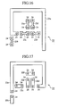
- Fig. 15 is a top cross-sectional view of a multi-layered inductance element according to a second embodiment of the present invention, showing conductor line patterns of the multi-layered inductance element.
- symbol 1b designates a dielectric substrate
- 22 designates a first conductor line pattern
- 23 designates second conductor line pattern
- 24 designates through-holes.
- the embodiment of the multi-layered inductance element also includes multi-layered dielectric substrates as similar to the structure of the first embodiment shown in Fig. 2.
- Upper and lower ground conducting layers are disposed on the upper surface of the uppermost dielectric substrate and the lower surface of the lowermost surface of the dielectric substrate.
- the side cross-sectional view of the multi-layered inductance element is similar to Fig. 2.
- Fig. 15 is a cross-sectional view taken along line I-I in Fig. 2, similarly to Fig. 1.
- the dielectric substrate 1b shown in Fig. 15 is the intermediate dielectric substrate among the multi-layered inductance element.
- the first conductor line pattern 22 is disposed on a surface of the dielectric substrate 1b and is interposed between the dielectric substrate 1b and another dielectric substrate.
- the second conductor line pattern 13 is disposed on another surface of the dielectric substrate 1b and is interposed between the dielectric substrate 1b and a further dielectric substrate.
- the through-holes 24 are formed to penetrate the dielectric substrate 1b, resulting in that the conductor line patterns 22 and 23 on the upper and lower surfaces of the dielectric substrate 1b are electrically connected with each other via conducting materials inside the through-holes 24.
- Fig. 15 depict parts of the conductor line patterns 22 and 23 overlapping with or superimposed over each other.
- the second conductor line pattern 23 and first conductor line pattern 22 will be described in more detail with reference to Figs. 16 and 17.
- the second conductor line pattern 23 includes a plurality of (for example, six) second line segments 23a through 23f being apart from one another.
- the second conductor line pattern 23 has substantially five gaps where adjacent first conductor line segments are spaced apart.
- the second conductor line pattern 23 exhibits a substantially looped configuration as a whole if the adjacent second line segments 23b, 23a, 23d, 23f, 23e, and 23c are interconnected.
- the longest second line segment 23a includes four straight parts having a uniform width, and itself exhibits a looped configuration although it is not closed completely.
- Each of the other second line segments 23b through 23f extends linearly, but only both end parts thereof have the same width as that of the second line segment 23a while the halfway part thereof is coarctate.
- the second line segments 23b through 23f are equivalent to the second line segments 13b and 13c of the first embodiment. As best shown in Fig. 16, while the second line segments 23b, 23e, and 23f extend in the ordinate direction, the second line segments 23c and 23d extends in the abscissa direction. Consequently, three second line segments 23b, 23e, and 23f are angled at 90 degrees with two second line segments 23c and 23d.
- the first conductor line pattern 22 includes a plurality of (for example, six) first line segments 22a through 22f being apart from one another.
- the first conductor line pattern 22 has substantially five gaps where adjacent second conductor line segments are spaced apart. All of the first line segments 22a through 22f are located on a surface of the dielectric substrate 1b, which is opposite to the surface on which the second line segments 23a through 23f are located.
- the first conductor line pattern 22 exhibits a substantially looped configuration as a whole if the adjacent first line segments 22b, 22a, 22d, 22f, 22e, and 22c are interconnected.
- first line segments 22a through 22f the longest first line segment 22a includes four straight parts having a uniform width, and itself exhibits a looped configuration although it is not closed completely.
- Each of the other first line segments 22b through 22f extends straightly and has a rectangular shape with a uniform width that is the same as that of the first line segment 22a.
- These first line segments 22b through 22f are equivalent to the first line segments 12b and 12c in the first embodiment.
- the first line segments 22c and 22f extends in the abscissa direction. Consequently, three first line segments 22b, 22e, and 22d are angled at 90 degrees with two first line segments22c and 22f.
- hatched parts in Fig. 15 depict parts of the conductor line patterns 22 and 23 overlapping with or superimposed over each other.
- Each of the first line segments 22a through 22f extends over at least a part of one of the second line segments 23a through 23f. Especially, end parts of the first and second line segments are placed over each other.
- an end part of the first line segment 22b at the bottom left-hand corner in Fig. 15 extends over one end part of the second line segment 23b while the other end part of the second line segment 23b extends over one end part of the first line segment 22a.
- the other end part of the first line segment 22a extends over one end part of the second line segment 23d while the other end part of the second line segment 23d extends over one end part of the first line segment 22d.
- the other end part of the first line segment 22d extends over one end part of the second line segment 23f while the other end part of the second line segment 23f extends over one end part of the first line segment 22f.
- the other end part of the first line segment 22f extends over one end part of the second line segment 23e while the other end part of the second line segment 23e extends over one end part of the first line segment 22e.
- the other end part of the first line segment 22e extends over one end part of the second line segment 23c while the other end part of the second line segment 23c extends over one end part of the first line segment 22c.
- the other end part of the first line segment 22c extends over one end part of the second line segment 23a while most of the second line segment 23a extends over most of the first line segment 22a.
- the overlapping end parts are electrically interconnected via one of the through-holes 24.
- the line segments cooperate to form a single continuous spiral conductor line, which is analogous to a coil, having an inductance.
- the direction of the current flow in the first conductor line pattern 22 is the same as that in the second conductor line pattern 23, for example, it is the clockwise direction as indicated by arrow I in Fig. 15.
- the direction of the current flow at each moment in the first conductor line pattern 22 is the same as that in the second conductor line pattern 23.
- the first conductor line pattern 22 contains five gaps where adjacent first conductor line segments are spaced apart. More specifically, there are the gaps in parts A1 through A3 and B1 and B2 enclosed by dashed lines in Fig. 15: the first gap is interposed between the first line segments 22b and 22a in part A1, the second is between the first line segments 22d and 22f in part A2, the third is between the first line segments 22f and 22e in part A3, the fourth is between the first line segments 22a and 22d in part B1, the last is between the first line segments 22e and 22c in part B2.
- the second conductor line segment 23b extending over the gap in part A1 for connecting the adjacent first line segments 22b and 22a; the second conductor line segment 23f extending over the gap in part A2 for connecting the adjacent first line segments 22d and 22f; and the second conductor line segments23e extending over the gap in part A3 for connecting the adjacent first line segments 22f and 22e are angled at 90 degrees with the second line segments 23d extending over the gap in part B 1 for connecting the first conductor line segments 22a and 22d; and the second conductor line segment 23d extending over the gap in part B2 for connecting the first line segments 22e and 22c.
- the total inductance of the multi-layered inductance element is increased by virtue of the narrower halfway parts of the second line segments 23b, 23f, and 23e in parts A1, A2, and A3.
- the inductance increment resulting from parts A1, A2, and A3 may compensate for the inductance decrement as a result of the coupling weakening of electromagnetic fields around two conductors, which are not coincident with each other.
- a plurality of parts A1, A2, and A3 are provided for restraining the impedance variation due to the relative dislocation of the conductor line patterns 22 and 23 in X direction.
- the impedance depends on the configurations of the conductor line patterns 22 and 23, it is possible to remarkably restrain variation of the total inductance in the multi-layered inductance element in comparison with another embodiment including only a single part for restraining impedance variation.
- the total inductance of the multi-layered inductance element is increased by virtue of the narrower halfway parts of the second line segments 23d and 23c in parts B1 and B2.
- the inductance increment resulting from parts B1 and B2 may compensate for the inductance decrement as a result of the coupling weakening of electromagnetic fields around two conductors, which are not coincident with each other.
- a plurality of parts B1 and B2 are provided for restraining the impedance variation due to the relative dislocation of the conductor line patterns 22 and 23 in Y direction.
- the impedance depends on the configurations of the conductor line patterns 22 and 23, it is possible to remarkably restrain variation of the total inductance in the multi-layered inductance element in comparison with another embodiment including only a single part for restraining impedance variation.
- the plurality of through-holes 24 become the factors for canceling the inductance variation. Therefore, it is also possible to restrain variation of inductance of the multi-layered inductance element.
- the number of the through-holes 24 is increased. This also contributes to remarkably restrain variation of the total inductance in the multi-layered inductance element although the inductance also depends on the configurations of the conductor line patterns 22 and 23.
- the impedance depends on the configurations of the conductor line patterns 22 and 23, it is possible to remarkably restrain variation of the total inductance in the multi-layered inductance element.
- two conductor line patterns on both surfaces of the intermediate dielectric substrate, and the through-holes penetrating through the dielectric substrate comprise a single spiral conductor line.
- two or more intermediate dielectric substrates may be provided and conductor line patterns on the respective intermediate dielectric substrates along with through-holes penetrating through the respective intermediate dielectric substrates may comprise a single spiral conductor line.
- the structure according to the present invention may be applied to such a modified configuration.
Landscapes
- Engineering & Computer Science (AREA)
- Power Engineering (AREA)
- Microelectronics & Electronic Packaging (AREA)
- Manufacturing & Machinery (AREA)
- Coils Or Transformers For Communication (AREA)
Abstract
On each surface of a dielectric substrate (1b), arranged are a first
conductor line pattern (12, 22) having a plurality of first line segments
(12a-12c, 22a-22f) and a second conductor line pattern (13, 23) having a
plurality of second line segments (13a-13c, 23a-23f). Ends of each first
conductor line segment overlap the second conductor line segments, and the
first and second line segments are connected via through-holes (14a-14e, 24),
thereby forming a single spiral conductor line. Each second conductor line
segment for connecting adjacent first conductor line segments has a pair of
end parts connected to the first conductor line segments via through-holes
and a halfway part having a smaller width.
Description
- The present invention relates to a multi-layered inductance element.
- Layered inductance elements have been utilized in radio frequency circuits or other electric circuits. As disclosed in JP-A-5-267973, a conventional multi-layered inductance element includes a plurality of layered dielectric substrates and looped conductor lines interposed therebetween. The looped conductor lines are interconnected via through-holes, thereby exhibiting a spiral configuration as a whole.
- Figs. 18 and 19 illustrate an example of conventional multi-layered inductance elements. As shown in the drawings, the multi-layered inductance element includes a plurality of
dielectric substrates conductor lines hole 4, and a pair ofground conducting layers ground conducting layer 5 is provided on the top surface of the uppermost dielectric substrate 1a among the multi-layereddielectric substrates layer 6 is disposed on the bottom surface of the lowermostdielectric substrates 1c. - The
upper conductor line 2 is interposed between thedielectric substrates 1a and 1b while thelower conductor line 3 is interposed between thedielectric substrates hole 4 is formed in the intermediatedielectric substrate 1b, resulting in that the upper andlower conductor lines hole 4. - As shown in Fig. 18, each of the
conductor lines conductor lines conductor line 2 is connected with one end of theconductor line 3 via the through-hole 4,conductor lines conductor line 2 is the same as that in theconductor line 3; for example, it is the clockwise direction as indicated by arrow I in Fig. 18. In addition, when an alternating current is applied, the direction of the current flow at each moment in theconductor line 2 is the same as that in theconductor line 3. - In connection with this kind of multi-layered inductance element, it has been considered that the upper and
lower conductor lines conductor lines conductor lines - In the illustrated conventional multi-layered inductance element, each of the
conductor lines hole 4 is utilized for connecting the upper andlower conductor lines - The conventional multi-layered inductance element structured as described above has drawbacks that it is difficult to restrain the difference between the designed target inductance and the resulting inductance affected by an error in dimensions by manufacturing. It is also very difficult to adjust or tune the difference.
- The drawbacks will be described in more detail. In such a multi-layered inductance element, the correlation between the positions of the
conductor lines conductor lines conductor lines conductor lines - In addition, if the thickness of the
dielectric substrate 1b and hence the distance between theconductor lines conductor lines dielectric substrate 1b is large, the inductance is decreased. - Accordingly, dimensional errors, such as positional errors of the
conductor lines dielectric substrate 1b, lead variations of inductance in products of multi-layered inductance element. - Accordingly, it is an object of the present invention to provide a multi-layered inductance element, wherein it is possible to restrain variations of inductance caused by errors in dimensions by manufacturing.
- A multi-layered inductance element according to the present invention includes at least one dielectric substrate having a first and second surfaces, a first conductor line pattern, a second conductor line pattern, and a plurality of through-holes penetrating through the dielectric substrate. The first conductor line pattern includes a plurality of first conductor line segments being apart from each other and disposed on the first surface of the dielectric substrate, wherein the first conductor line segments exhibit a substantially looped configuration as a whole if adjacent first conductor line segments are connected with each other. The second conductor line pattern includes a plurality of second conductor line segments being apart from each other and disposed on the second surface of the dielectric substrate, wherein the second conductor line segments exhibit a substantially looped configuration as a whole if adjacent second conductor line segments are connected with each other. Each through-hole electrically connects one end of one of the first conductor line segments and one end of one of the second conductor line segments. Each of the first conductor line segments extends over at least a part of one of the second conductor line segments. The plurality of first conductor line segments and the plurality of second conductor line segments are connected by the through-holes, thereby forming a spiral conductor line in which a direction of current flow in the first conductor line pattern is the same as that in the second conductor line pattern. Each of the second conductor line segments includes a pair of end parts and a halfway part having a width which is smaller than that of the end parts. The end parts are connected to adjacent first conductor line segments via the through-holes.
- With such a structure, the halfway part with a smaller width of each second conductor line element tends to cancel an inductance decrement when the conductor line patterns are dislocated in relation to each other. In addition, the plurality of through-holes contributes to cancel an inductance variation when the thickness of the dielectric substrate varies. Therefore, the structure can restrain variations of inductance caused by errors in dimensions by manufacturing multi-layered inductance elements.
- With reference to the accompanying drawings, various embodiments of the present invention will be described hereinafter. In the drawings,
- Fig. 1 is a top cross-sectional view of a multi-layered inductance element according to a first embodiment of the present invention, showing conductor line patterns of the multi-layered inductance element;
- Fig. 2 is a cross-sectional view taken along line II-II in Fig. 1;
- Fig. 3 is a plane view representing a second conductor line pattern in the multi-layered inductance element of Fig. 1 in detail;
- Fig. 4 is a plane view representing a first conductor line pattern in the multi-layered inductance element of Fig. 1 in detail;
- Fig. 5 is an enlarged view of part A in Fig. 1;
- Fig. 6 is a schematic diagram showing a circuit equivalent to the structure shown in Fig. 5;
- Fig. 7 is an enlarged view of part Ain Fig. 1 when a positional error of conductor occurs in the abscissa direction;
- Fig. 8 is a schematic diagram showing a circuit equivalent to the structure shown in Fig. 7;
- Fig. 9 is an enlarged view of part Ain Fig. 1 when a positional error of conductor occurs in the ordinate direction;
- Fig. 10 is a schematic diagram showing a circuit equivalent to the structure shown in Fig. 9;
- Fig. 11 is a schematic diagram showing a circuit equivalent to the structure of part A in Fig. 1 when the thickness of the dielectric substrate varies;
- Fig. 12 is an enlarged view showing a variant of part A;
- Fig. 13 is an enlarged view showing another variant of part A;
- Fig. 14 is an enlarged view showing a further variant of part A;
- Fig. 15 is a top cross-sectional view of a multi-layered inductance element according to a second embodiment of the present invention, showing conductor line patterns of the multi-layered inductance element;
- Fig. 16 is a plane view representing a second conductor line pattern in the multi-layered inductance element of Fig. 15 in detail;
- Fig. 17 is a plane view representing a first conductor line pattern in the multi-layered inductance element of Fig. 15 in detail;
- Fig. 18 is a top cross-sectional view of a conventional multi-layered inductance element, showing conductor line patterns of the multi-layered inductance element; and
- Fig. 19 is a cross-sectional view taken along line XIV-XIV in Fig. 18.
-
- Fig. 1 is a top cross-sectional view of a multi-layered inductance element according to a first embodiment of the present invention, showing conductor line patterns of the multi-layered inductance element. Fig. 2 is a side cross-sectional view of the multi-layered inductance element. More exactly, Fig. 1 is a cross-sectional view taken along line I-I in Fig. 2 while Fig. 2 is a cross-sectional view taken along line II-II in Fig. 1.
- As shown in the drawings, the multi-layered inductance element includes
dielectric substrates conductor line pattern 12, a secondconductor line pattern 13, andground conducting layers conductor line pattern 12 includes a plurality offirst line segments 12a through 12c while the secondconductor line pattern 13 includes a plurality ofsecond line segments 13a through 13c connected to thefirst line segments 12a through 12c via through-holes 14a through 14e. - As represented in Fig. 2, the upper
ground conducting layer 5 is provided on the top surface of the uppermost dielectric substrate 1a among the multi-layereddielectric substrates ground conducting layer 6 is disposed on the bottom surface of the lowermostdielectric substrates 1c. - The first
conductor line pattern 12 is interposed between thedielectric substrates 1a and 1b while the secondconductor line pattern 13 is interposed between thedielectric substrates dielectric substrate 1b, the through-holes 14a through 14e are formed to penetrate thedielectric substrate 1b, resulting in that theconductor line patterns dielectric substrate 1b are electrically connected with each other via conducting materials inside the through-holes 14a through 14e. - As shown in Fig. 1, each of the
conductor line patterns conductor line patterns conductor line pattern 13 and firstconductor line pattern 12 will be described in more detail with reference to Figs. 3 and 4. - As represented in Fig. 3, the second
conductor line pattern 13 includes a plurality of (for example, three)second line segments 13a through 13c being apart from one another. In other words, the secondconductor line pattern 13 has two gaps where adjacent first conductor line segments are spaced apart. All of thesecond line segments 13a through 13c are located on a surface of thedielectric substrate 1b. - Among those
second line segments 13a through 13c, the longestsecond line segment 13a includes four straight parts having a uniform width. In thesecond line segment 13a, the upper ends of two straight parts extending in parallel along the ordinate direction in Fig. 3 are connected at right angles with each end of the upper straight part extending along the abscissa direction. The lower end of the left straight part extending along the ordinate direction in Fig. 3 is connected at a right angle with an end of the lower shortest straight part extending along the abscissa direction. The lower shortest straight part extending along the abscissa direction is directed toward the right longest straight part extending along the ordinate direction. Accordingly, thesecond line segment 13a itself exhibits a looped configuration although it is not closed completely. - Another
second line segment 13b is aligned in the extending direction of the left straight part of thesecond line segment 13a. Although thesecond line segment 13b extends straightly, only both end parts thereof have the same width as that of thesecond line segment 13a while the halfway part thereof is coarctate. - A further
second line segment 13c is aligned in the extending direction of the lower straight part of thesecond line segment 13a. Accordingly, the shortsecond line segment 13c is angled at 90 degrees with the shortsecond line segment 13b. Although thesecond line segment 13c extends straightly, only both end parts thereof have the same width as that of thesecond line segment 13a while the halfway part thereof is coarctate. As illustrated, thesecond line segments second line segments - The second
conductor line pattern 13 exhibits a substantially looped configuration as a whole if the adjacentsecond line segments second line segments - Referring now to Fig. 4, the first
conductor line pattern 12 includes a plurality of (for example, three)first line segments 12a through 12c being apart from one another. In other words, the firstconductor line pattern 12 has two gaps where adjacent second conductor line segments are spaced apart. All of thefirst line segments 12a through 12c are located on a surface of thedielectric substrate 1b, which is opposite to the surface on which thesecond line segments 13a through 13c are located. - Among those
first line segments 12a through 12c, the longestfirst line segment 12a includes four straight parts having a uniform width. In thefirst line segment 12a, the upper ends of two straight parts extending in parallel along the ordinate direction in Fig. 4 are connected at right angles with each end of the upper straight part extending along the abscissa direction. The lower end of the right straight part extending along the ordinate direction in Fig. 4 is connected at a right angle with an end of the lower shortest straight part extending along the abscissa direction. The lower shortest straight part extending along the abscissa direction is directed toward the left longest straight part extending along the ordinate direction. Accordingly, thefirst line segment 12a itself exhibits a looped configuration although it is not closed completely. - A shorter
first line segment 12b is aligned in the extending direction of the left straight part of thefirst line segment 12a. Thefirst line segment 12b extends straightly and has a uniform width that is the same as that of thefirst line segment 12a. - Another shorter
first line segment 12c is aligned in the extending direction of the lower straight part of thefirst line segment 12a. Accordingly, thefirst line segment 12c is angled at 90 degrees with thefirst line segment 12b. Thefirst line segment 12c extends straightly and has a uniform width that is the same as that of thefirst line segment 12a. - The first
conductor line pattern 12 also exhibits a looped configuration as a whole if the adjacentfirst line segments first line segments - As described above, the hatched parts in Fig. 1 depict parts of the
conductor line patterns first line segments 12a through 12c extends over at least a part of one of thesecond line segments 13a through 13c. Especially, end parts of the first and second line segments are placed over each other, and the overlapping end parts are electrically interconnected via any of the through-holes 14a through 14e. - More specifically, most of the
first line segment 12b at the bottom left-hand corner in Fig. 1 extends over one end part of thesecond line segment 13b, and the overlapping parts are interconnected via the through-hole 14c. The other end part of thesecond line segment 13b extends over one end part of thefirst line segment 12a, and the overlapping parts are interconnected via the through-hole 14b. The other end part of thefirst line segment 12a extends over an end part of thesecond line segment 13c, and the overlapping parts are interconnected via the through-hole 14d. The other end part of thesecond line segment 13c extends over an end part of thefirst line segment 12c, and the overlapping parts are interconnected via the through-hole 14e. The other end part of thefirst line segment 12c extends over an end part of thesecond line segment 13a, and the overlapping parts are interconnected via the through-holes 14a. Most of thesecond line segment 13a extends over most of thefirst line segment 12a. In connection with the overlapping parts, it is preferable that the side edges of bothline segments - By the interconnection between the first and second
conductor line patterns holes 14a through 14e, theline segments conductor line pattern 12 is the same as that in the secondconductor line pattern 13; for example, it is the clockwise direction as indicated by arrow I in Fig. 1. In addition, when an alternating current is applied, the direction of the current flow at each moment in the firstconductor line pattern 12 is the same as that in the secondconductor line pattern 13. - In the multi-layered inductance element, the first
conductor line pattern 12 contains two gaps where adjacent first conductor line segments are spaced apart. More specifically, there are the gaps in parts A and B enclosed by dashed lines in Fig. 1: one is interposed between thefirst line segments first line segments second line segment 13b extending over the gap in part A for connecting the adjacentfirst line segments second line segment 13c extending over the gap in part B for connecting the adjacent firstconductor line segments - Fig. 5 is an enlarged view of part A in Fig. 1. As will be apparent from observation of part A illustrated in Fig. 5, the
first line segment 12a is connected with thefirst line segment 12b via the through-hole 14b, the wider end part of thesecond line segment 13b, the coarctate halfway part of thesecond line segment 13b having a width W, the other wider end part of thesecond line segment 13b, and the through-hole 14c. - Let us assume that Fig. 5 shows the
second line segment 13b formed at an ideal location in relation to thefirst line segments second line segment 13b coincide perfectly with the side edges of thefirst line segments second line segment 13b coincide perfectly with the end edge of thefirst line segment - Next, operations will be described. Fig. 6 is a schematic diagram showing a circuit equivalent to the structure shown in Fig. 5. In Fig. 6, L1 and L2 indicate the inductance values of the through-
holes second line segment 13b having a smaller width W. L3 and L4 indicate the inductance values of both end parts of thesecond line segment 13b, respectively. - Fig. 7 represents the same structure as that shown in Fig. 5, but shows the
second line segment 13b dislocated in relation to thefirst line segments second line segment 13b, respectively. - In the structure shown in Fig. 7, the distance between each through-
hole second line segment 13b is broader than that in Fig. 5, so as to increase the inductance, whereby L3b > L3 and L4b > L4. However, the inductance values L1, L2, and L5 do not vary in connection with the structures in Figs. 5 and 7 since the shapes and dimensions of the corresponding parts are the same. In X direction, the larger the dislocating amount of thesecond line segment 13b is, the larger the distance between each of the through-holes second line segment 13b is, so that the inductance values L3b and L4b are increased. - The width W is in inverse proportion to the increments L3b - L3 and L4b - L4 caused by the dislocation, i.e., positional error in X direction. Therefore, the shorter the width W is, the larger the increments of inductance are.
- Fig. 9 also represents the same structure as that shown in Fig. 5, but shows the
second line segment 13b dislocated in relation to thefirst line segments second line segment 13b, respectively. - When the
second line segment 13b is dislocated in relation to thefirst line segments hole second line segment 13b also vary. However, the increment of one of the distances is exactly equal to the decrement of the other distance, so that L3c + L4c = L3 + L4. Accordingly, the total inductance in the circuit is kept unchanged. - Next, an inductance variation when the thickness of the
dielectric substrate 1b is reduced in the structure in Fig. 5 will be described. Fig. 11 shows a circuit equivalent to the structure of part A when the thickness of the dielectric substrate is reduced. Lid and L2d in Fig. 11, which correspond to L1 and L2 in Fig. 6, are inductance values of the through-holes - The length of a through-hole is proportional to the inductance thereof. Accordingly, if the thickness of the
dielectric substrate 1b and hence the length of the through-holes holes dielectric substrate 1b is larger, L1d > L1 and L2d > L2. - On the other hand, the inductance of a through-hole tends to increase as the diameter thereof is reduced. Accordingly, the inductance increments L1d - L1 and L2d - L2 can be finely or slightly tuned or adjusted by changing the diameters of the through-
holes - As described above, as the dislocating amount of the
second line segment 13b increases in relation to thefirst line segments second line segment 13b is in inverse proportion to the increment of inductance caused by the dislocation, i.e., positional error in X direction. Therefore, the increment of inductance can be finely or slightly tuned or adjusted by altering the width W. - As to the structure within part A shown in Fig. 3, the total inductance is kept unchanged even if the
second line segment 13b is dislocated in Y direction. If the thickness of thedielectric substrate 1b varies, the total inductance tends to vary. However, the variation can be finely or slightly tuned or adjusted by changing the diameters of the through-holes - Returning now to Fig. 1, let us observe the entire structure of the multi-layered inductance element. In the entire multi-layered inductance element in Fig. 1 except for parts A and B, if the
conductor line patterns - However, as described above, if the
conductor line patterns second line segment 13b having the halfway part with a smaller width becomes the factor of increase of total inductance. Accordingly, it is possible to restrain a variation of inductance caused by a relative dislocation or positional error of theconductor line patterns - It is preferable to design the multi-layered inductance element, especially the
second line segment 13b, in ideal dimensions so that the inductance increment resulting from thesecond line segment 13b balances with the inductance decrement resulting from other parts in order to maintain the total inductance unchanged completely at any degree of relative dislocation of theconductor line patterns - Furthermore, in an optional process, it is possible to finely or slightly tune or adjust the inductance increment in X direction resulting from the
second line segment 13b by adjusting the width W of the halfway part of thesecond line segment 13b. In this case, the relation between relative dislocations of theconductor line patterns conductor line patterns conductor line patterns dielectric substrate 1b. On the basis of the measurement and the above-described relation, the width W of the halfway part of thesecond line segment 13b may be modified, so that the variation of the total inductance of the multi-layered inductance element may be minimized. - On the other hand, if there is a relative dislocation of the
conductor line patterns second line segment 13c having the halfway part with a smaller width becomes the factor of increase of total inductance. Accordingly, it is possible to restrain a variation of inductance with respect to a relative dislocation or positional error of theconductor line patterns - It is preferable to design the multi-layered inductance element, especially the
second line segment 13c, in ideal dimensions so that the inductance increment resulting from thesecond line segment 13c balances with the inductance decrement resulting from other parts in order to maintain the total inductance unchanged completely at any degree of relative dislocation of theconductor line patterns - Furthermore, in an optional process, it is possible to finely or slightly tune or adjust the inductance increment in Y direction resulting from the
second line segment 13c by adjusting the width W of the halfway part of thesecond line segment 13c. In this case, the relation between relative dislocations of theconductor line patterns conductor line patterns conductor line patterns dielectric substrate 1b. On the basis of the measurement and the above-described relation, the width W of the halfway part of thesecond line segment 13c may be modified, so that the variation of the total inductance of the multi-layered inductance element may be minimized. - Furthermore, when the multi-layered inductance element except for parts A and B in Fig. 1 is analyzed, if the thickness of the
dielectric substrate 1b and hence the distance between theconductor line patterns dielectric substrate 1b is large, the inductance is decreased. This problem has been also discussed in conjunction with prior art. - However, as described above, the length of a through-hole is proportional to the inductance thereof. Consequently, as long as effects of the through-holes, if the thickness of the
dielectric substrate 1b is smaller, the inductance values are decreased. On the contrary, if the thickness of thedielectric substrate 1b is larger, the inductance values of the through-holes are increased. Since the embodiment of the multi-layered inductance element is provided with parts A and B, the multi-layered inductance element includes a plurality of through-holes 14a through 14e, which are more than those in usual structure, resulting in that the spiral conductor line meanders in the vertical direction (direction in the thickness) of the multi-layered inductance element. - Accordingly, even if most of the overlapping
conductor line patterns dielectric substrate 1b, the plurality of through-holes 14a through 14e become the factors for canceling the inductance variation. Therefore, it is also possible to restrain variation of inductance of the multi-layered inductance element. - It is preferable to design the multi-layered inductance element, especially the through-
holes 14a through 14e, in ideal configurations so that the inductance variation resulting from the overlappingconductor line patterns holes 14a through 14e in order to maintain the total inductance unchanged completely at any degree of thickness variation of thedielectric substrate 1b. - Furthermore, in an optional process, it is possible to finely or slightly tune or adjust the inductance variation resulting from the through-
holes 14a through 14e by adjusting the one or more diameters of the through-holes 14a through 14e. In this case, the relation between the thickness of thedielectric substrate 1b and total inductance values of the multi-layered inductance element is preferably obtained by, e.g., an experiment. At a stage in the manufacturing process, the thickness of thedielectric substrate 1b is measured after thedielectric substrate 1b has been formed. On the basis of the measurement and the above-described relation, the diameter(s) of any or all of the through-holes 14a through 14e may be modified, so that the variation of the total inductance of the multi-layered inductance element may be minimized. - As described above, the first embodiment may restrain variation of inductance caused by an error in dimensions by manufacturing, such as a relative dislocation or positional error of the
conductor line patterns dielectric substrate 1b. Especially, since thesecond line segments conductor line patterns - In the illustrated first embodiment, the adjacent
first line segments second line segment 13b connecting them are aligned linearly in part A. The same is true for part B containing the adjacentfirst line segments conductor line segment 13c connecting them. However, it is not intended to limit the present invention to the illustrated arrangement in first embodiment. Rather, other suitable arrangements may be accepted as follows. - Figs. 12 through 14 show variants of part A. In the variant of part A in Fig. 12, the
second line segment 13b and thefirst line segment 12b are aligned in straight in the ordinate direction while thefirst line segment 12a is disposed in the abscissa direction, forming an angle of 90 degrees with them. - In the variant of part A in Fig. 13, the
first line segments second line segment 13b is disposed in the ordinate direction, forming an angle of 90 degrees with them. Thefirst line segment 12a extends rightward from the end that is connected with thesecond line segment 13b while thefirst line segment 12b extends leftward oppositely. - In the variant of part A in Fig. 14, the
first line segments second line segment 13b is disposed in the ordinate direction, forming an angle of 90 degrees with them. Thefirst line segment 12a extends leftward from the end that is connected with thesecond line segment 13b and thefirst line segment 12b extends leftward similarly. - These variants achieve the same advantageous effects as those described above. Similar variants may be utilized for part B.
- Fig. 15 is a top cross-sectional view of a multi-layered inductance element according to a second embodiment of the present invention, showing conductor line patterns of the multi-layered inductance element. In Fig. 15,
symbol 1b designates a dielectric substrate, 22 designates a first conductor line pattern, 23 designates second conductor line pattern, and 24 designates through-holes.Reference symbols 22a through 22f depict first line segments belonging to the firstconductor line pattern conductor line pattern 23. - The embodiment of the multi-layered inductance element also includes multi-layered dielectric substrates as similar to the structure of the first embodiment shown in Fig. 2. Upper and lower ground conducting layers are disposed on the upper surface of the uppermost dielectric substrate and the lower surface of the lowermost surface of the dielectric substrate. Thus, the side cross-sectional view of the multi-layered inductance element is similar to Fig. 2. Fig. 15 is a cross-sectional view taken along line I-I in Fig. 2, similarly to Fig. 1. The
dielectric substrate 1b shown in Fig. 15 is the intermediate dielectric substrate among the multi-layered inductance element. - The first
conductor line pattern 22 is disposed on a surface of thedielectric substrate 1b and is interposed between thedielectric substrate 1b and another dielectric substrate. The secondconductor line pattern 13 is disposed on another surface of thedielectric substrate 1b and is interposed between thedielectric substrate 1b and a further dielectric substrate. In the intermediatedielectric substrate 1b, the through-holes 24 are formed to penetrate thedielectric substrate 1b, resulting in that theconductor line patterns dielectric substrate 1b are electrically connected with each other via conducting materials inside the through-holes 24. - The hatched parts in Fig. 15 depict parts of the
conductor line patterns conductor line pattern 23 and firstconductor line pattern 22 will be described in more detail with reference to Figs. 16 and 17. - As represented in Fig. 16, the second
conductor line pattern 23 includes a plurality of (for example, six)second line segments 23a through 23f being apart from one another. In other words, the secondconductor line pattern 23 has substantially five gaps where adjacent first conductor line segments are spaced apart. The secondconductor line pattern 23 exhibits a substantially looped configuration as a whole if the adjacentsecond line segments - Among those
second line segments 23a through 23f, the longestsecond line segment 23a includes four straight parts having a uniform width, and itself exhibits a looped configuration although it is not closed completely. Each of the othersecond line segments 23b through 23f extends linearly, but only both end parts thereof have the same width as that of thesecond line segment 23a while the halfway part thereof is coarctate. Thesecond line segments 23b through 23f are equivalent to thesecond line segments second line segments second line segments second line segments second line segments - Referring now to Fig. 17, the first
conductor line pattern 22 includes a plurality of (for example, six)first line segments 22a through 22f being apart from one another. In other words, the firstconductor line pattern 22 has substantially five gaps where adjacent second conductor line segments are spaced apart. All of thefirst line segments 22a through 22f are located on a surface of thedielectric substrate 1b, which is opposite to the surface on which thesecond line segments 23a through 23f are located. The firstconductor line pattern 22 exhibits a substantially looped configuration as a whole if the adjacentfirst line segments - Among those
first line segments 22a through 22f, the longestfirst line segment 22a includes four straight parts having a uniform width, and itself exhibits a looped configuration although it is not closed completely. Each of the otherfirst line segments 22b through 22f extends straightly and has a rectangular shape with a uniform width that is the same as that of thefirst line segment 22a. Thesefirst line segments 22b through 22f are equivalent to thefirst line segments first line segments first line segments first line segments - As described above, the hatched parts in Fig. 15 depict parts of the
conductor line patterns first line segments 22a through 22f extends over at least a part of one of thesecond line segments 23a through 23f. Especially, end parts of the first and second line segments are placed over each other. - More specifically, an end part of the
first line segment 22b at the bottom left-hand corner in Fig. 15 extends over one end part of thesecond line segment 23b while the other end part of thesecond line segment 23b extends over one end part of thefirst line segment 22a. The other end part of thefirst line segment 22a extends over one end part of thesecond line segment 23d while the other end part of thesecond line segment 23d extends over one end part of thefirst line segment 22d. The other end part of thefirst line segment 22d extends over one end part of thesecond line segment 23f while the other end part of thesecond line segment 23f extends over one end part of thefirst line segment 22f. The other end part of thefirst line segment 22f extends over one end part of thesecond line segment 23e while the other end part of thesecond line segment 23e extends over one end part of thefirst line segment 22e. The other end part of thefirst line segment 22e extends over one end part of thesecond line segment 23c while the other end part of thesecond line segment 23c extends over one end part of thefirst line segment 22c. The other end part of thefirst line segment 22c extends over one end part of thesecond line segment 23a while most of thesecond line segment 23a extends over most of thefirst line segment 22a. - The overlapping end parts are electrically interconnected via one of the through-
holes 24. By the interconnection between the first and secondconductor line patterns holes 24, the line segments cooperate to form a single continuous spiral conductor line, which is analogous to a coil, having an inductance. When a direct current is applied to the spiral conductor line, the direction of the current flow in the firstconductor line pattern 22 is the same as that in the secondconductor line pattern 23, for example, it is the clockwise direction as indicated by arrow I in Fig. 15. In addition, when an alternating current is applied, the direction of the current flow at each moment in the firstconductor line pattern 22 is the same as that in the secondconductor line pattern 23. - In the multi-layered inductance element, the first
conductor line pattern 22 contains five gaps where adjacent first conductor line segments are spaced apart. More specifically, there are the gaps in parts A1 through A3 and B1 and B2 enclosed by dashed lines in Fig. 15: the first gap is interposed between thefirst line segments first line segments first line segments first line segments first line segments conductor line segment 23b extending over the gap in part A1 for connecting the adjacentfirst line segments conductor line segment 23f extending over the gap in part A2 for connecting the adjacentfirst line segments first line segments second line segments 23d extending over the gap inpart B 1 for connecting the firstconductor line segments conductor line segment 23d extending over the gap in part B2 for connecting thefirst line segments - In accordance with the embodiment, when there is a relative dislocation or positional error of the
conductor line patterns second line segments conductor line patterns conductor line patterns - In addition, when there is a relative dislocation or positional error of the
conductor line patterns second line segments conductor line patterns conductor line patterns - Furthermore, even if most of the overlapping
conductor line patterns dielectric substrate 1b, the plurality of through-holes 24 become the factors for canceling the inductance variation. Therefore, it is also possible to restrain variation of inductance of the multi-layered inductance element. In accordance with the embodiment, as a result of provision of a greater number of parts A1, A2, A3, B1, and B2, the number of the through-holes 24 is increased. This also contributes to remarkably restrain variation of the total inductance in the multi-layered inductance element although the inductance also depends on the configurations of theconductor line patterns - As described above, in accordance with the second embodiment, although the impedance depends on the configurations of the
conductor line patterns - In the first and second embodiments, two conductor line patterns on both surfaces of the intermediate dielectric substrate, and the through-holes penetrating through the dielectric substrate comprise a single spiral conductor line. However, two or more intermediate dielectric substrates may be provided and conductor line patterns on the respective intermediate dielectric substrates along with through-holes penetrating through the respective intermediate dielectric substrates may comprise a single spiral conductor line. The structure according to the present invention may be applied to such a modified configuration.
- While the present invention has been particularly shown and described with references to preferred embodiments thereof, it will be understood by those skilled in the art that various changes in form and details may be made therein without departing from the spirit and scope of the invention as defined by the claims. Such variations, alterations, and modifications are intended to be encompassed in the scope of the claims.
Claims (3)
- A multi-layered inductance element comprising:wherein each of the first conductor line segments extends over at least a part of one of the second conductor line segments, the plurality of first conductor line segments being connected with the plurality of second conductor line segments via the through-holes, thereby forming a spiral conductor line in which a direction of current flow in the first conductor line pattern is the same as that in the second conductor line pattern,at least one dielectric substrate (1b) having a first and second surfaces;a first conductor line pattern (12, 22) including a plurality of first conductor line segments (12a-12c, 22a-22f) being apart from each other and disposed on the first surface of the dielectric substrate, wherein the first conductor line segments exhibit a substantially looped configuration as a whole if adjacent first conductor line segments are connected with each other;a second conductor line pattern (13, 23) including a plurality of second conductor line segments (13a-13c, 23a-23f) being apart from each other and disposed on the second surface of the dielectric substrate, wherein the second conductor line segments exhibit a substantially looped configuration as a whole if adjacent second conductor line segments are connected with each other; anda plurality of through-holes (14a-14e, 24) penetrating through the dielectric substrate, each through-hole electrically connecting one end of one of the first conductor line segments and one end of one of the second conductor line segments,
and wherein each of the second conductor line segments includes a pair of end parts and a halfway part having a width which is smaller than that of the end parts, the end parts being connected to adjacent first conductor line segments via the through-holes. - The multi-layered inductance element as recited in claim 1, wherein the first conductor line pattern (12, 22) contains at least two gaps where adjacent first conductor line segments (12a-12c, 22a-22f) are spaced apart, two second conductor line segments (13a-13c, 23a-23f) being disposed over the two gaps, respectively, and wherein one of the second conductor line segments over one of the gaps for connecting two adjacent first conductor line segments is angled at 90 degrees with the other of the second conductor line segments over the other of the gaps for connecting two adjacent first conductor line segments.
- The multi-layered inductance element as recited in claim 2, wherein the first conductor line pattern (22) contains at least four gaps where adjacent first conductor line segments (22a-22f) are spaced apart, four second conductor line segments (23a-23f) being disposed over the four gaps, and wherein two of the second conductor line segments over two of the gaps for connecting adjacent first conductor line segments are angled at 90 degrees with the other two of the second conductor line segments over the other two of the gaps for connecting adjacent first conductor line segments.
Applications Claiming Priority (2)
| Application Number | Priority Date | Filing Date | Title |
|---|---|---|---|
| JP2001381994A JP3634305B2 (en) | 2001-12-14 | 2001-12-14 | Multilayer inductance element |
| JP2001381994 | 2001-12-14 |
Publications (1)
| Publication Number | Publication Date |
|---|---|
| EP1320109A1 true EP1320109A1 (en) | 2003-06-18 |
Family
ID=19187400
Family Applications (1)
| Application Number | Title | Priority Date | Filing Date |
|---|---|---|---|
| EP02017813A Withdrawn EP1320109A1 (en) | 2001-12-14 | 2002-08-07 | Multi-layered inductance element |
Country Status (4)
| Country | Link |
|---|---|
| US (1) | US6657530B2 (en) |
| EP (1) | EP1320109A1 (en) |
| JP (1) | JP3634305B2 (en) |
| KR (1) | KR100475620B1 (en) |
Families Citing this family (4)
| Publication number | Priority date | Publication date | Assignee | Title |
|---|---|---|---|---|
| CN101765893B (en) * | 2007-07-30 | 2012-10-10 | 株式会社村田制作所 | Chip Coil Components |
| JP5223821B2 (en) * | 2009-08-28 | 2013-06-26 | Tdk株式会社 | Multilayer electronic components |
| JP5994933B2 (en) * | 2013-05-08 | 2016-09-21 | 株式会社村田製作所 | Electronic components |
| CN114724799B (en) * | 2021-01-06 | 2024-06-04 | 瑞昱半导体股份有限公司 | Inductance device |
Citations (5)
| Publication number | Priority date | Publication date | Assignee | Title |
|---|---|---|---|---|
| EP0484558A1 (en) * | 1990-05-25 | 1992-05-13 | Murata Manufacturing Co., Ltd. | High frequency coil and method of manufacturing the same |
| EP0631293A1 (en) * | 1993-06-24 | 1994-12-28 | Telecontrolli S.P.A. | Planar inductor and method of operatively calibrating the same in a RF system |
| US6124779A (en) * | 1996-12-11 | 2000-09-26 | Murata Manufacturing Co. Ltd. | Multilayer-type inductor |
| US6175293B1 (en) * | 1988-09-30 | 2001-01-16 | Kabushiki Kaisha Toshiba | Planar inductor |
| US20010041401A1 (en) * | 1999-02-26 | 2001-11-15 | Kie Y. Ahn | Open pattern inductor |
Family Cites Families (11)
| Publication number | Priority date | Publication date | Assignee | Title |
|---|---|---|---|---|
| US4021705A (en) * | 1975-03-24 | 1977-05-03 | Lichtblau G J | Resonant tag circuits having one or more fusible links |
| JPH0377360A (en) | 1989-08-18 | 1991-04-02 | Mitsubishi Electric Corp | Semiconductor device |
| JPH04148514A (en) | 1990-10-12 | 1992-05-21 | Murata Mfg Co Ltd | Adjusting method of inductance of printed coil |
| JP2695342B2 (en) * | 1992-03-19 | 1997-12-24 | ティーディーケイ株式会社 | Hybrid coupler |
| JP3132786B2 (en) * | 1992-08-19 | 2001-02-05 | 太陽誘電株式会社 | Multilayer chip inductor and method of manufacturing the same |
| TW262595B (en) * | 1993-11-17 | 1995-11-11 | Ikeda Takeshi | |
| JP3601096B2 (en) * | 1994-09-22 | 2004-12-15 | 株式会社村田製作所 | Manufacturing method of multilayer inductor |
| US6175727B1 (en) * | 1998-01-09 | 2001-01-16 | Texas Instruments Israel Ltd. | Suspended printed inductor and LC-type filter constructed therefrom |
| KR20000040049A (en) * | 1998-12-17 | 2000-07-05 | 김춘호 | Stacked Chip Inductors |
| JP2001044035A (en) * | 1999-07-30 | 2001-02-16 | Murata Mfg Co Ltd | Multilayer inductor |
| KR20000059248A (en) * | 2000-07-26 | 2000-10-05 | 엄우식 | Laminated complex chip of combining with resistor and inductor and fabricating method therefor |
-
2001
- 2001-12-14 JP JP2001381994A patent/JP3634305B2/en not_active Expired - Fee Related
-
2002
- 2002-06-06 US US10/162,635 patent/US6657530B2/en not_active Expired - Fee Related
- 2002-08-07 EP EP02017813A patent/EP1320109A1/en not_active Withdrawn
- 2002-08-13 KR KR10-2002-0047711A patent/KR100475620B1/en not_active Expired - Fee Related
Patent Citations (5)
| Publication number | Priority date | Publication date | Assignee | Title |
|---|---|---|---|---|
| US6175293B1 (en) * | 1988-09-30 | 2001-01-16 | Kabushiki Kaisha Toshiba | Planar inductor |
| EP0484558A1 (en) * | 1990-05-25 | 1992-05-13 | Murata Manufacturing Co., Ltd. | High frequency coil and method of manufacturing the same |
| EP0631293A1 (en) * | 1993-06-24 | 1994-12-28 | Telecontrolli S.P.A. | Planar inductor and method of operatively calibrating the same in a RF system |
| US6124779A (en) * | 1996-12-11 | 2000-09-26 | Murata Manufacturing Co. Ltd. | Multilayer-type inductor |
| US20010041401A1 (en) * | 1999-02-26 | 2001-11-15 | Kie Y. Ahn | Open pattern inductor |
Also Published As
| Publication number | Publication date |
|---|---|
| US20030112115A1 (en) | 2003-06-19 |
| JP2003188017A (en) | 2003-07-04 |
| US6657530B2 (en) | 2003-12-02 |
| JP3634305B2 (en) | 2005-03-30 |
| KR20030051162A (en) | 2003-06-25 |
| KR100475620B1 (en) | 2005-03-15 |
Similar Documents
| Publication | Publication Date | Title |
|---|---|---|
| KR100939755B1 (en) | Stacked Baluns and Hybrid Integrated Circuit Modules and Stacked Boards | |
| US8907757B2 (en) | Common mode choke coil and high-frequency electronic device | |
| US8044749B1 (en) | Coupler device | |
| US20120161897A1 (en) | Directional coupler | |
| US8711055B2 (en) | Printed circuit board including electromagnetic bandgap structure | |
| US20050253677A1 (en) | Coil component | |
| US11869701B2 (en) | Circuit element | |
| US20060097820A1 (en) | Printed circuit board built-in type planar balun and method for manufacturing same | |
| KR101792274B1 (en) | Filter for Removing Noise | |
| EP1320109A1 (en) | Multi-layered inductance element | |
| JP6847814B2 (en) | Printed wiring board | |
| US12518902B2 (en) | Coil component | |
| WO2000079846A1 (en) | Transition between symmetric stripline and asymmetric stripline | |
| US11831292B2 (en) | LC composite component and communication terminal device | |
| JP7505601B2 (en) | Directional Coupler | |
| US7525397B2 (en) | Stripline directional coupler having a wide coupling gap | |
| US12525379B2 (en) | Coil component | |
| EP3676907B1 (en) | Radio frequency (rf) coupler | |
| US20230307167A1 (en) | Multilayer coil component | |
| JP7840190B2 (en) | Electronic components | |
| JP2005012559A (en) | Coupler and coupler array | |
| US20240305007A1 (en) | Transmission line arrangement for a passive component | |
| CN116453824A (en) | Laminated coil component | |
| KR100550906B1 (en) | Stacked LC Filter Arrays | |
| JP2005018627A (en) | Data transfer circuit board |
Legal Events
| Date | Code | Title | Description |
|---|---|---|---|
| PUAI | Public reference made under article 153(3) epc to a published international application that has entered the european phase |
Free format text: ORIGINAL CODE: 0009012 |
|
| AK | Designated contracting states |
Designated state(s): AT BE BG CH CY CZ DE DK EE ES FI FR GB GR IE IT LI LU MC NL PT SE SK TR |
|
| AX | Request for extension of the european patent |
Extension state: AL LT LV MK RO SI |
|
| 17P | Request for examination filed |
Effective date: 20030827 |
|
| AKX | Designation fees paid |
Designated state(s): DE FR GB |
|
| RAP1 | Party data changed (applicant data changed or rights of an application transferred) |
Owner name: MITSUBISHI DENKI KABUSHIKI KAISHA |
|
| STAA | Information on the status of an ep patent application or granted ep patent |
Free format text: STATUS: THE APPLICATION HAS BEEN WITHDRAWN |
|
| 18W | Application withdrawn |
Effective date: 20060818 |