EP1317994B1 - Positioniereinrichtung für Halbleiterobjekte - Google Patents
Positioniereinrichtung für Halbleiterobjekte Download PDFInfo
- Publication number
- EP1317994B1 EP1317994B1 EP02026440A EP02026440A EP1317994B1 EP 1317994 B1 EP1317994 B1 EP 1317994B1 EP 02026440 A EP02026440 A EP 02026440A EP 02026440 A EP02026440 A EP 02026440A EP 1317994 B1 EP1317994 B1 EP 1317994B1
- Authority
- EP
- European Patent Office
- Prior art keywords
- positioning device
- semiconductor
- semiconductor object
- region
- holder
- Prior art date
- Legal status (The legal status is an assumption and is not a legal conclusion. Google has not performed a legal analysis and makes no representation as to the accuracy of the status listed.)
- Expired - Lifetime
Links
Images



Classifications
-
- H—ELECTRICITY
- H10—SEMICONDUCTOR DEVICES; ELECTRIC SOLID-STATE DEVICES NOT OTHERWISE PROVIDED FOR
- H10P—GENERIC PROCESSES OR APPARATUS FOR THE MANUFACTURE OR TREATMENT OF DEVICES COVERED BY CLASS H10
- H10P72/00—Handling or holding of wafers, substrates or devices during manufacture or treatment thereof
- H10P72/70—Handling or holding of wafers, substrates or devices during manufacture or treatment thereof for supporting or gripping
- H10P72/76—Handling or holding of wafers, substrates or devices during manufacture or treatment thereof for supporting or gripping using mechanical means, e.g. clamps or pinches
- H10P72/7602—Handling or holding of wafers, substrates or devices during manufacture or treatment thereof for supporting or gripping using mechanical means, e.g. clamps or pinches the wafers being placed on a robot blade or gripped by a gripper for conveyance
-
- G—PHYSICS
- G01—MEASURING; TESTING
- G01N—INVESTIGATING OR ANALYSING MATERIALS BY DETERMINING THEIR CHEMICAL OR PHYSICAL PROPERTIES
- G01N21/00—Investigating or analysing materials by the use of optical means, i.e. using sub-millimetre waves, infrared, visible or ultraviolet light
- G01N21/84—Systems specially adapted for particular applications
- G01N21/88—Investigating the presence of flaws or contamination
- G01N21/95—Investigating the presence of flaws or contamination characterised by the material or shape of the object to be examined
- G01N21/9501—Semiconductor wafers
Definitions
- a bracket is used which is articulated to carry out the movements.
- Actuators in the form of plungers transmit the Movements to the bracket of one, in its inclination adjustable ring with a rotatable spindle is concentrically coupled.
- the disadvantage is that by the Use of tappets caused limitation of the Movement range for the bracket.
- the movement of a pressure element can either on a circular path or consist of two in succession assemble running partial movements, one of which first parallel to the surface of the semiconductor object and a second is directed perpendicular to this surface.
- the associated swivel axis S runs also through the center M and is parallel to one Adjustment plane X-Y directed, the one in the reference system occupies a horizontal position.
- One in the adjustment plane X-Y adjustable and rotatable about the z-axis, not X-Y- ⁇ table shown can be provided to the Bear bow guide 5.
- the swivel axis S falls with the turning axis W. together.
- the z axis and thus the adjustment plane X-Y can be used with the present positioning device also a Rotational movement around the z-axis and translatory x-y movements be overlaid in the adjustment plane X-Y.
- the one used to hold the semiconductor object 1 frame-shaped object holder 2 points in the present case the holder of a semiconductor wafer has a ring structure on, which encloses a free space with the center M, the in size and shape of the semiconductor object to be held 1 is adjusted.
- An open area 6 also serves one Access with an edge-handling device during the feeding and removal of the semiconductor object 1 like a partial expansion of the ring structure one to the outside, to the open area 6 opposite ring section 7.
- the semiconductor object 1 is advantageously placed on one of two inclined slopes in the edge region thereof.
- the other bevel is provided for the contact of the pressure element 13, which is also similar in material to that of the support 12, so that damage to the edge of the semiconductor object 1 and its coating are avoided.
- the pressure element 13 has in its front area a pressure cone 18 designed as a transition cone with a transitional cone angle or concave radius, so that the pre-adjusted semiconductor object 1 is completely centered during the clamping process (FIG. 4).
- a resilient area 19 adjoining the pressure cone 18 has an advantageous effect on the clamping properties of the holding mechanisms 8, 9, 10 and 11.
- a constant current is used in the pressure phase, which current can be set for each pressure element 13 and generates the necessary pressure force.
- the motors are driven with a constant voltage which can be set for each operating phase and which can additionally be set by the external digital voltage control 31. All electrical components and connections are arranged on a printed circuit board 34, the shape of which is adapted to the structure of the object holder 2.
Landscapes
- Physics & Mathematics (AREA)
- Health & Medical Sciences (AREA)
- Life Sciences & Earth Sciences (AREA)
- Chemical & Material Sciences (AREA)
- Analytical Chemistry (AREA)
- Biochemistry (AREA)
- General Health & Medical Sciences (AREA)
- General Physics & Mathematics (AREA)
- Immunology (AREA)
- Pathology (AREA)
- Container, Conveyance, Adherence, Positioning, Of Wafer (AREA)
Description
Derartige Einrichtungen sind insbesondere zu Inspektionszwecken einsetzbar.
- Fig. 1
- ein schematisiertes Bewegungssystem einer erfindungsgemäßen Positioniereinrichtung
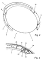
- Fig. 2
- einen verkleideten Objekthalter für die Positioniereinrichtung in einer perspektivischen Darstellung von oben
- Fig. 3
- die Anordnung eines Haltemechanismus innerhalb des Objekthalters und eines Sensorteiles zur Lagekontrolle des Halbleiterobjektes
- Fig. 4
- die Halterung eines Halbleiterobjektes, betrachtet aus der Richtung des Freiraumes
- Fig. 5
- ein Antriebssystem für einen Haltemechanismus
- Fig. 6
- das teilweise unverkleidete Antriebssystem
- Fig. 7
- Sensorenstrahlengänge zur Lagekontrolle des Halbleiterobjektes
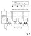
- Fig. 8
- ein Blockschaltbild zur elektrischen Steuerung der Haltemechanismen
Ein sich an den Andruckkegel 18 anschließender federnder Bereich 19 wirkt sich vorteilhaft auf die Klemmeigenschaften der Haltemechanismen 8, 9, 10 und 11 aus. Mit dem gewissermaßen als "Klemmfinger" ausgebildeten Andruckelement 13 wird eine minimale Federwirkung beim Kantenandruck und eine Reduzierung von Rückwirkungskräften in seinen Antrieb 20 aufgrund des zwischengeschalteten federnden Bereiches 19 erreicht. Der Antrieb 20 ist ein Miniatur-Gleichstrommotor mit Untersetzungsgetriebe und für die Reinraumtauglichkeit in einer Partikelschutzkappe 21 gekapselt. Das Andruckelement 13 wird durch eine Schenkelfeder 22 (Fig. 6) mit einer zur Objekthalterung ausreichenden Minimalkraft in seiner Andruckposition gehalten, so dass auch bei Ausfall der Energieversorgung das Halbleiterobjekt 1 sicher geklemmt bleibt. Der Gleichstrommotor unterstützt die Feder beim Schließvorgang zum Herstellen der Klemmung und spannt diese beim Aufheben der Klemmung. Auch die Schenkelfeder 22 und deren Arbeitsraum ist partikelsicher durch ein Federgehäuse 23 gekapselt.
- Verlassen der Offenposition
- Schnelles Heranfahren des Andruckelementes 13 an die Klemmposition
- Synchronisationspause aller vier Andruckelemente 13 mit einem Zwangsstop der Antriebe 20, um ein gleichmäßiges Andrücken und optimales Zentrieren zu erreichen und schließlich einem
- Andrücken der Andruckelemente 13 an das Halbleiterobjekt 1.
- einem langsamen Entspannen des Andruckes
- einem schnellen Freifahren des Andruckelementes 13 und
- einem Halten der Schenkelfeder 18 in der Offenposition.
Die Andruckphase ausgenommen, werden die Motoren mit einer für jede Betriebsphase einstellbaren Konstantspannung angetrieben, die zusätzlich durch die externe digitale Spannungssteuerung 31 eingestellt werden kann.
Alle elektrischen Bauelemente und Verbindungen sind auf einer Leiterplatte 34 angeordnet, die in der Form an die Struktur des Objekthalters 2 angepasst ist.
Claims (10)
- Positioniereinrichtung für Halbleiterobjekte mit einem rahmenförmigen Objekthalter zur Aufnahme eines Halbleiterobjektes, wobei der rahmenförmige Objekthalter (2) einen Freiraum für die Aufnahme des Halbleiterobjektes (1) umschließt sowie in einer Auflageebene befindliche Auflagen (12) und zwischen zwei Endpositionen verstellbare Andruckelemente (13) zur Halterung des Halbleiterobjektes (1) in dessen Randbereich enthält, dadurch gekennzeichnet, dass jedes Andruckelement (13) in dem Objekthalter (2) mit einem Antrieb (20) verbunden ist, der eine Bewegung des Andruckelementes (13) in einer Ebene erzeugt, die senkrecht zu der Auflageebene gerichtet ist, wobei das Halbleiterobjekt (1) in einer Endposition (K) an der Auflage fixiert ist und in der anderen Endposition (F), bei der das Andruckelement (13) aus dem Freiraum herausgenommen ist, zur Handhabung freigegeben ist.
- Positioniereinrichtung nach Anspruch 1, dadurch gekennzeichnet, dass die Bewegung des Andruckelementes (13) auf einer Kreisbahn erfolgt.
- Positioniereinrichtung nach Anspruch 2, dadurch gekennzeichnet, dass die Bewegung aus zwei nacheinander ablaufenden Teilbewegungen zusammengesetzt ist, von denen eine erste parallel zur Oberfläche des Halbleiterobjektes (1) und eine zweite senkrecht zu dieser Oberfläche gerichtet ist.
- Positioniereinrichtung nach Anspruch 3, dadurch gekennzeichnet, dass jedes der Andruckelemente (13) einen zentrierenden Andruckkegel (18) mit federnden Eigenschaften aufweist.
- Positioniereinrichtung nach Anspruch 4, dadurch gekennzeichnet, dass die federnden Eigenschaften durch einen Bereich (19) aus elastischem Material bestimmt sind.
- Positioniereinrichtung nach einem der Ansprüche 2 bis 5, dadurch gekennzeichnet, dass jede der Auflagen (12) mit einem Zentrierkegel (15) versehen ist, dessen Kegelform in einen sphärischen Auflagebereich (16) für das Halbleiterobjekt (1) übergeht.
- Positioniereinrichtung nach Anspruch 6, dadurch gekennzeichnet, dass dem sphärischen Auflagebereich (16) unterhalb ein Auffangbereich zur Verhinderung eines Durchrutschen oder einer Beschädigung des Halbleiterobjektes 1 bei einer fehlerhaften Übergabe benachbart ist.
- Positioniereinrichtung nach einem der Ansprüche 2 bis 7, dadurch gekennzeichnet, dass jeder der Antriebe (20) mit einem Schaltelement (27) versehen ist, das in den Endpositionen Endlagensensoren (24, 25) betätigt.
- Positioniereinrichtung nach einem der Ansprüche 2 bis 8, dadurch gekennzeichnet, dass der Objekthalter (2) mindestens einen Sensor (28, 29) zum Nachweis einer verkippungsfreien Lage des Halbleiterobjektes (1) enthält, dessen Sensorstrahlengang durch eine zu einer Auflageebene für das Halbleiterobjekt (1) parallel gerichteten Ebene gelegt ist.
- Positioniereinrichtung nach einem der Ansprüche 2 bis 9, dadurch gekennzeichnet, dass der Objekthalter (2) als Ringstruktur ausgebildet ist, die einen offenen Bereich (6) für eine kantengreifende Handhabungseinrichtung zur Zuführung und Entnahme des Halbleiterobjektes (1) enthält und gegenüberliegend zu dem offenen Bereich durch einen versetzten Ringabschnitt (7) partiell erweitert ist.
Applications Claiming Priority (2)
| Application Number | Priority Date | Filing Date | Title |
|---|---|---|---|
| DE10160521A DE10160521B4 (de) | 2001-12-05 | 2001-12-05 | Positioniereinrichtungen für Halbleiterobjekte |
| DE10160521 | 2001-12-05 |
Publications (3)
| Publication Number | Publication Date |
|---|---|
| EP1317994A2 EP1317994A2 (de) | 2003-06-11 |
| EP1317994A3 EP1317994A3 (de) | 2003-08-13 |
| EP1317994B1 true EP1317994B1 (de) | 2004-11-10 |
Family
ID=7708617
Family Applications (1)
| Application Number | Title | Priority Date | Filing Date |
|---|---|---|---|
| EP02026440A Expired - Lifetime EP1317994B1 (de) | 2001-12-05 | 2002-11-27 | Positioniereinrichtung für Halbleiterobjekte |
Country Status (2)
| Country | Link |
|---|---|
| EP (1) | EP1317994B1 (de) |
| DE (2) | DE10160521B4 (de) |
Families Citing this family (2)
| Publication number | Priority date | Publication date | Assignee | Title |
|---|---|---|---|---|
| CN114823441B (zh) * | 2022-06-28 | 2022-09-02 | 深圳市星国华先进装备科技有限公司 | 一种针测机传输机构晶圆防滑出保护装置 |
| CN117246736B (zh) * | 2023-10-27 | 2024-03-29 | 上海广川科技有限公司 | 一种晶圆回旋翻转机构及其回旋翻转方法 |
Family Cites Families (6)
| Publication number | Priority date | Publication date | Assignee | Title |
|---|---|---|---|---|
| US5096291A (en) * | 1990-05-16 | 1992-03-17 | Irvine Optical Corporation | Inspection systems having rotating motion |
| DE19821007A1 (de) * | 1998-05-11 | 1999-11-25 | Steag Rtp Systems Gmbh | Verfahren und Vorrichtung zum thermischen Behandeln von Substraten |
| US6204917B1 (en) * | 1998-09-22 | 2001-03-20 | Kla-Tencor Corporation | Backside contamination inspection device |
| DE19947174A1 (de) * | 1998-10-12 | 2000-04-13 | Ims Ionen Mikrofab Syst | Halteeinrichtung für eine Maske |
| DE10003639C2 (de) * | 2000-01-28 | 2003-06-18 | Steag Rtp Systems Gmbh | Vorrichtung zum thermischen Behandeln von Substraten |
| DE10028569A1 (de) * | 2000-06-09 | 2001-12-13 | Brooks Automation Gmbh | Vorrichtung zum Positionieren scheibenförmiger Objekte |
-
2001
- 2001-12-05 DE DE10160521A patent/DE10160521B4/de not_active Expired - Fee Related
-
2002
- 2002-11-27 EP EP02026440A patent/EP1317994B1/de not_active Expired - Lifetime
- 2002-11-27 DE DE50201507T patent/DE50201507D1/de not_active Expired - Fee Related
Also Published As
| Publication number | Publication date |
|---|---|
| EP1317994A3 (de) | 2003-08-13 |
| DE10160521A1 (de) | 2003-12-18 |
| DE50201507D1 (de) | 2004-12-16 |
| DE10160521B4 (de) | 2004-09-30 |
| EP1317994A2 (de) | 2003-06-11 |
Similar Documents
| Publication | Publication Date | Title |
|---|---|---|
| AT405775B (de) | Verfahren und vorrichtung zum ausgerichteten zusammenführen von scheibenförmigen halbleitersubstraten | |
| DE69415517T3 (de) | Handhabungseinrichtung mit gelenkarm | |
| DE19524025C2 (de) | Spindelanordnungen mit Waferhalter | |
| DE3688957T2 (de) | Verfahren und vorrichtung zum erfassen der halterungsstellung eines elektrischen gerätes und montierungsvorrichtung eines elektronischen gerätes. | |
| DE2556098C2 (de) | Vorrichtung zum Einsetzen eines Stiftes in ein Loch eines Werkstückes | |
| DE68919234T2 (de) | Vorrichtung zum Vorwählen und festhalten einer festen Distanz zwischen einem Werkstück und einem Vakuumgerät in Partikelstrahllithographiesystemen. | |
| DE69806326T2 (de) | Gelenkroboter | |
| DE102018107247A1 (de) | Ladungspartikelstrahlvorrichtung | |
| DE3011002A1 (de) | Werkzeugverbindungsmechanismus fuer werkzeugmaschinen | |
| DE69422700T2 (de) | Waferhalteplatte und hebevorrichtung | |
| DE3829022A1 (de) | Tischverstellvorrichtung | |
| DE19549045C1 (de) | Einrichtung zur Handhabung von scheibenförmigen Objekten | |
| DE69026172T2 (de) | Behandlungsposten für kompakte Muster | |
| DE112015002397T5 (de) | Automatische Handhabungsvorrichtung | |
| DE102013105945A1 (de) | Bearbeitungskopf für eine Laserbearbeitungsmaschine sowie Laserbearbeitungsmaschine und Verfahren zum Wechsel eines Schutzglases im Bearbeitungskopf | |
| DE102012014558A1 (de) | Kinematisches Haltesystem für einen Bestückkopf einer Bestückvorrichtung | |
| DE102004005574B3 (de) | Robotersystem mit Werkzeug, Kamera und Lichtquelle | |
| EP1238410A1 (de) | Vorrichtung und verfahren zum ausrichten von scheibenförmigen substraten | |
| DE112013002039B4 (de) | Vorrichtung mit einer optischen Röntgenkomponente und Röntgenanalysator | |
| WO2019201558A1 (de) | Adapter für ein objektiv, vorrichtung zum halten des adapters und stellvorrichtung | |
| DE10160521B4 (de) | Positioniereinrichtungen für Halbleiterobjekte | |
| DE3931305C2 (de) | Prüfsondenkartenhalterung | |
| DE10028569A1 (de) | Vorrichtung zum Positionieren scheibenförmiger Objekte | |
| DE19947174A1 (de) | Halteeinrichtung für eine Maske | |
| EP1527662B1 (de) | Vorrichtung zum selektiven bewegen von haltevorrichtungen und best ckkopf zum transportieren von bauelementen |
Legal Events
| Date | Code | Title | Description |
|---|---|---|---|
| PUAI | Public reference made under article 153(3) epc to a published international application that has entered the european phase |
Free format text: ORIGINAL CODE: 0009012 |
|
| AK | Designated contracting states |
Designated state(s): AT BE BG CH CY CZ DE DK EE ES FI FR GB GR IE IT LI LU MC NL PT SE SK TR |
|
| AX | Request for extension of the european patent |
Extension state: AL LT LV MK RO SI |
|
| PUAL | Search report despatched |
Free format text: ORIGINAL CODE: 0009013 |
|
| AK | Designated contracting states |
Designated state(s): AT BE BG CH CY CZ DE DK EE ES FI FR GB GR IE IT LI LU MC NL PT SE SK TR |
|
| AX | Request for extension of the european patent |
Extension state: AL LT LV MK RO SI |
|
| 17P | Request for examination filed |
Effective date: 20031030 |
|
| GRAP | Despatch of communication of intention to grant a patent |
Free format text: ORIGINAL CODE: EPIDOSNIGR1 |
|
| AKX | Designation fees paid |
Designated state(s): DE FR GB |
|
| GRAS | Grant fee paid |
Free format text: ORIGINAL CODE: EPIDOSNIGR3 |
|
| GRAA | (expected) grant |
Free format text: ORIGINAL CODE: 0009210 |
|
| AK | Designated contracting states |
Kind code of ref document: B1 Designated state(s): DE FR GB |
|
| PG25 | Lapsed in a contracting state [announced via postgrant information from national office to epo] |
Ref country code: GB Free format text: LAPSE BECAUSE OF FAILURE TO SUBMIT A TRANSLATION OF THE DESCRIPTION OR TO PAY THE FEE WITHIN THE PRESCRIBED TIME-LIMIT Effective date: 20041110 |
|
| REG | Reference to a national code |
Ref country code: GB Ref legal event code: FG4D Free format text: NOT ENGLISH |
|
| REG | Reference to a national code |
Ref country code: IE Ref legal event code: FG4D Free format text: GERMAN |
|
| REF | Corresponds to: |
Ref document number: 50201507 Country of ref document: DE Date of ref document: 20041216 Kind code of ref document: P |
|
| PG25 | Lapsed in a contracting state [announced via postgrant information from national office to epo] |
Ref country code: DE Free format text: LAPSE BECAUSE OF NON-PAYMENT OF DUE FEES Effective date: 20050601 |
|
| GBV | Gb: ep patent (uk) treated as always having been void in accordance with gb section 77(7)/1977 [no translation filed] |
Effective date: 20041110 |
|
| REG | Reference to a national code |
Ref country code: IE Ref legal event code: FD4D |
|
| PLBE | No opposition filed within time limit |
Free format text: ORIGINAL CODE: 0009261 |
|
| STAA | Information on the status of an ep patent application or granted ep patent |
Free format text: STATUS: NO OPPOSITION FILED WITHIN TIME LIMIT |
|
| 26N | No opposition filed |
Effective date: 20050811 |
|
| ET | Fr: translation filed | ||
| REG | Reference to a national code |
Ref country code: FR Ref legal event code: PLFP Year of fee payment: 14 |
|
| REG | Reference to a national code |
Ref country code: FR Ref legal event code: PLFP Year of fee payment: 15 |
|
| PGFP | Annual fee paid to national office [announced via postgrant information from national office to epo] |
Ref country code: FR Payment date: 20161118 Year of fee payment: 15 |
|
| REG | Reference to a national code |
Ref country code: FR Ref legal event code: ST Effective date: 20180731 |
|
| PG25 | Lapsed in a contracting state [announced via postgrant information from national office to epo] |
Ref country code: FR Free format text: LAPSE BECAUSE OF NON-PAYMENT OF DUE FEES Effective date: 20171130 |