EP1316142B1 - Digitaler phasen- und amplitudenmodulator, und verfahren dazu - Google Patents
Digitaler phasen- und amplitudenmodulator, und verfahren dazu Download PDFInfo
- Publication number
- EP1316142B1 EP1316142B1 EP01984282A EP01984282A EP1316142B1 EP 1316142 B1 EP1316142 B1 EP 1316142B1 EP 01984282 A EP01984282 A EP 01984282A EP 01984282 A EP01984282 A EP 01984282A EP 1316142 B1 EP1316142 B1 EP 1316142B1
- Authority
- EP
- European Patent Office
- Prior art keywords
- modulation
- signal
- cmi
- control signals
- scji2
- Prior art date
- Legal status (The legal status is an assumption and is not a legal conclusion. Google has not performed a legal analysis and makes no representation as to the accuracy of the status listed.)
- Expired - Lifetime
Links
- 238000000034 method Methods 0.000 title claims abstract description 31
- 230000010363 phase shift Effects 0.000 claims abstract description 14
- 230000000295 complement effect Effects 0.000 claims description 23
- 230000000737 periodic effect Effects 0.000 claims description 3
- 238000011144 upstream manufacturing Methods 0.000 claims description 2
- JBRZTFJDHDCESZ-UHFFFAOYSA-N AsGa Chemical compound [As]#[Ga] JBRZTFJDHDCESZ-UHFFFAOYSA-N 0.000 description 4
- 229910001218 Gallium arsenide Inorganic materials 0.000 description 4
- 230000006978 adaptation Effects 0.000 description 4
- 238000010586 diagram Methods 0.000 description 4
- 238000006073 displacement reaction Methods 0.000 description 4
- 230000005669 field effect Effects 0.000 description 4
- 238000010276 construction Methods 0.000 description 3
- 239000013598 vector Substances 0.000 description 3
- 101100210170 Saccharomyces cerevisiae (strain ATCC 204508 / S288c) VRP1 gene Proteins 0.000 description 2
- 238000005516 engineering process Methods 0.000 description 2
- 230000001939 inductive effect Effects 0.000 description 2
- 238000004519 manufacturing process Methods 0.000 description 2
- PCTMTFRHKVHKIS-BMFZQQSSSA-N (1s,3r,4e,6e,8e,10e,12e,14e,16e,18s,19r,20r,21s,25r,27r,30r,31r,33s,35r,37s,38r)-3-[(2r,3s,4s,5s,6r)-4-amino-3,5-dihydroxy-6-methyloxan-2-yl]oxy-19,25,27,30,31,33,35,37-octahydroxy-18,20,21-trimethyl-23-oxo-22,39-dioxabicyclo[33.3.1]nonatriaconta-4,6,8,10 Chemical compound C1C=C2C[C@@H](OS(O)(=O)=O)CC[C@]2(C)[C@@H]2[C@@H]1[C@@H]1CC[C@H]([C@H](C)CCCC(C)C)[C@@]1(C)CC2.O[C@H]1[C@@H](N)[C@H](O)[C@@H](C)O[C@H]1O[C@H]1/C=C/C=C/C=C/C=C/C=C/C=C/C=C/[C@H](C)[C@@H](O)[C@@H](C)[C@H](C)OC(=O)C[C@H](O)C[C@H](O)CC[C@@H](O)[C@H](O)C[C@H](O)C[C@](O)(C[C@H](O)[C@H]2C(O)=O)O[C@H]2C1 PCTMTFRHKVHKIS-BMFZQQSSSA-N 0.000 description 1
- GYHNNYVSQQEPJS-UHFFFAOYSA-N Gallium Chemical compound [Ga] GYHNNYVSQQEPJS-UHFFFAOYSA-N 0.000 description 1
- 240000008042 Zea mays Species 0.000 description 1
- 239000003990 capacitor Substances 0.000 description 1
- 150000001875 compounds Chemical class 0.000 description 1
- 230000006835 compression Effects 0.000 description 1
- 238000007906 compression Methods 0.000 description 1
- 239000006185 dispersion Substances 0.000 description 1
- 230000000694 effects Effects 0.000 description 1
- 238000005265 energy consumption Methods 0.000 description 1
- 229910052733 gallium Inorganic materials 0.000 description 1
- 238000010348 incorporation Methods 0.000 description 1
- 238000002955 isolation Methods 0.000 description 1
- 230000000873 masking effect Effects 0.000 description 1
- 238000012986 modification Methods 0.000 description 1
- 230000004048 modification Effects 0.000 description 1
Images

Classifications
-
- H—ELECTRICITY
- H03—ELECTRONIC CIRCUITRY
- H03C—MODULATION
- H03C7/00—Modulating electromagnetic waves
- H03C7/02—Modulating electromagnetic waves in transmission lines, waveguides, cavity resonators or radiation fields of antennas
- H03C7/025—Modulating electromagnetic waves in transmission lines, waveguides, cavity resonators or radiation fields of antennas using semiconductor devices
-
- H—ELECTRICITY
- H04—ELECTRIC COMMUNICATION TECHNIQUE
- H04L—TRANSMISSION OF DIGITAL INFORMATION, e.g. TELEGRAPHIC COMMUNICATION
- H04L27/00—Modulated-carrier systems
- H04L27/32—Carrier systems characterised by combinations of two or more of the types covered by groups H04L27/02, H04L27/10, H04L27/18 or H04L27/26
- H04L27/34—Amplitude- and phase-modulated carrier systems, e.g. quadrature-amplitude modulated carrier systems
- H04L27/36—Modulator circuits; Transmitter circuits
- H04L27/362—Modulation using more than one carrier, e.g. with quadrature carriers, separately amplitude modulated
Definitions
- the invention relates to a digital modulation method of a periodic carrier signal of high frequency -in particular being able to be in the microwave domain (frequency domain for which propagation phenomena are not negligible) - with a signal of digital modulation in general at lower frequency (i.e. less than that of the carrier signal), implemented by a modulator circuit comprising at least one modulation cell - in particular by phase displacement - intended to receive two digital control signals representative of at least minus part - notably a component - of the modulation signal digital. It extends to a modulating electronic circuit suitable for setting using such a method.
- WO-98.38730 describes an electronic modulator circuit by phase shift with distributed structure including a distribution line with n phase shift cells, a plurality of n parallel branches extending to from each phase shift cell and each comprising a circuit switch / modulator, and means for summing in phase the signals coming from switch / modulator circuits.
- the number of phase states that can be obtained can be greater than the number of branches when these have, at as a switch / modulator circuit, modulation cells which, in the most basic embodiment are modulation cells by phase shift with two phase states (called BPSK or MDP2) intended for receive two complementary digital control signals.
- the invention therefore aims to satisfy this need in a simple manner and economical. It aims in particular to propose a method and a circuit modulator for addressing a large number of points (phase states and / or amplitude) with zero power loss and low power consumption, so this circuit and process can be adapted and used with many types of coding and modulation, in many applications.
- the invention further aims to propose such a method and such a modulator circuit which are advantageously adapted to an embodiment in microwave monolithic technology (MMIC) -in particular on arsenide of gallium GaAs- with excellent accuracy.
- MMIC microwave monolithic technology
- the invention aims to allow a choice simple phase and / or amplitude states, at the very moment of its incorporation into the system (not during design or manufacturing of the integrated circuit itself).
- the invention further aims more particularly to propose such a method and such a modulator circuit compatible with the constraints of on-board space systems (small footprint, excellent reliability, low consumption).
- the invention also aims more particularly to propose a such a method and such a modulator circuit compatible with the codings of broadband modulation such as MCT, which become advantageous when one has a large number of phase states and / or amplitudes.
- the invention also aims more particularly to propose a such a method and such a modulator circuit can be adapted to any frequency of carrier signals, especially in the microwave field.
- the invention also aims more particularly to propose a such a method and such a modulator circuit which, after completion, can accept carrier input signals whose frequency is fixed, but can be chosen in a wide band (for example in the X band for telemetry Earth observation in the K-band of telecommunications satellites multimedia).
- the invention further aims to propose a modulation which does not not produce significant disturbances of the line and the input signal.
- the invention relates to a method of modulation of a carrier signal with a digital modulation signal at lower frequency, implemented by a modulator circuit comprising at at least one modulation cell intended to receive two control signals digital signals representing at least part of the modulation signal digital, characterized in that for at least one value of the signal digital modulation, at least one cell of modulation, two digital control signals of the same value.
- This modulation cell then provides, for this value of the modulation signal digital (for which digital control signals are the same value) a signal, called modulated elementary signal, which is different in amplitude and / or in phase - notably which is zero - of the one it provides when the signals numerical controls are complementary.
- the invention also extends to a circuit suitable for setting up work of the method according to the invention. It therefore also concerns a circuit modulator capable of modulating a carrier signal with a signal digital modulation at lower frequency, comprising at least one cell modulation for receiving two digital control signals representative of at least part of the digital modulation signal, characterized in that it is adapted so that, for at least one value of the signal digital modulation, at least one modulation cell receives two digital control signals of the same value.
- At least one modulation cell can be of the amplitude modulation according to a single phase state.
- at least one modulation cell is a modulation cell by phase displacement, the method and the circuit according to. the invention achieving digital modulation at least by displacement of phase.
- Each modulation cell can be a modulation by phase displacement of the type with two phase states (so-called cell BPSK or MDP2) - notably in opposition - generally having only one state of amplitude, but which can present as well two states of amplitude.
- cell BPSK or MDP2 phase states
- it is given one, or even two, additional phase and / or amplitude state (s).
- said modulation cell does not not provide the same modulated elementary signal when the control signals that it receives are equal to 0, and when they are equal to 1.
- This signal modulated elementary is not necessarily zero when the signals of numerical controls have the same value (both equal to 0 or 1).
- At least one modulation cell receiving two signals from digital commands of the same value for at least one value of the signal digital modulation is adapted to supply a signal, called elementary signal modulated, which is zero for this value of the digital modulation signal.
- At least a modulation cell is adapted to provide a modulated elementary signal with two opposing phase states and a single amplitude state when it receives complementary digital control signals, and to provide a modulated elementary signal which is zero when it receives control signals of the same value.
- each BPSK modulation cell provides a modulated signal which can present three, or even four, distinct values - in particular one of which is the null value -, and not only two values as in the case of a BPSK cell Traditional.
- the different modulated elementary signals of the different modulation cells are combined - notably summed in phase - to form the modulated output signal. It is thus possible to address a larger number of points in the Fresnel plane.
- a method according to the invention is characterized in that the modulator circuit comprises at least two cells of modulation, and in that, for at least one value of the modulation signal digital, two signal signals are applied to at least one modulation cell digital controls of the same value (this modulation cell providing preferably a modulated elementary signal which is zero for this value of the digital modulation signal), and apply to at least one other cell modulation, two digital value control signals complementary (this other modulation cell providing a signal modulated elementary which is not zero for this value of the modulation signal digital).
- At least one cell modulation provides a zero modulated elementary signal while at least one another provides a nonzero modulated elementary signal.
- a method according to the invention is also characterized in that for at least one value of the modulation signal digital, two signal signals are applied to at least one modulation cell numerical controls of the same value and in that for at least one other digital modulation signal value, apply to this (these) cell (s) of modulation two digital control signals of values complementary.
- the same modulation cell does not not provide a null modulated elementary signal for all the values of the signal of digital modulation.
- the digital control signals applied to the same cell modulation are both equal to 0. This avoids the drifts due to the technological imperfection of the electronic circuit which would not cancel the modulated elementary signal perfectly for two control signals numeric equals 1.
- the BPSK modulation cells traditional are well adapted in impedance when they receive complementary state control signals.
- the control signals take simultaneously the same value, and in particular both the value 0, in particular in the microwave domain.
- the inventors have, however, determined that it is in fact possible to provide means of impedance adaptation such as the impedance is in practice sufficiently adapted so that the signals of command are complementary or equal, in that the drifts caused by the impedance matching fault are less than, or same order as technological dispersions.
- a input signal from the carrier signal to each modulation cell by through adapted impedance matching means so that the cell modulation is at least substantially matched in impedance as well when the digital control signals it receives are complementary only when they are equal.
- the impedance matching means comprise for each cell of modulation a transistor which receives the input signal and is connected to the cell modulation, and a parallel resistance between the transistor and the ground.
- a modulator circuit is used with a distributed structure comprising several derived branches, each comprising at least one modulation cell intended to receive two digital control signals, each derived branch delivering a signal, called the output signal. of modulated branch, and summing in phase the modulated branch output signals from the different derivative branches to form a modulated output signal.
- a modulator circuit conforming to the distributed structure described in WO / 98.38730 is used.
- the number of phase states of each BPSK modulation cell is, in the process of the invention, not equal to 2 but to 3, which makes it possible to address with the modulated output signal 3 n points of the plane of Fresnel, n being the number of branches of the circuit (and not 2 n as in WO / 98.38730).
- a circuit according to the invention comprises advantageously upstream of each modulation cell, means impedance matching providing an input signal from the carrier signal to the modulation cell and adapted so that the modulation cell is at less substantially matched in impedance as well when the signals from digital commands it receives are complementary only when they are equal.
- the invention also relates to a method and a circuit. modulator characterized in combination by all or some of the characteristics mentioned above or below.
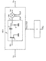
- the modulated output signal Ss is phase modulated as a function of the digital modulation signal SCj, for example of the NRZ type.
- ⁇ s ⁇ e.
- the modulator circuit 1 comprises at minus one CMi modulation cell per phase shift of the type intended to receive two representative digital control signals SCji1, SCji2 at least part of the modulation signal SCj.
- Such a CMi modulation cell can be formed of a traditional BPSK modulation cell with two opposite phase states and a single amplitude state (when the digital control signals are complementary).
- a CMi modulation cell is for example described in the publication A. PRIMEROSE et al. mentioned above ( Figure 3b) and includes two switches formed by field effect transistors and two input filters. at know a low-pass filter inducing a phase shift of -90 ° and a high-pass filter inducing a phase shift of + 90 °.
- these BPSK modulation cells are modified so as to be able to apply to them digital control signals SCji1, SCji2 of simultaneously identical values.
- these digital control signals are formed by the voltages Vg, and V g respectively.
- the digital control signals SCji1 and SCji2 are applied according to the invention to the gates, switching transistors CO0 and CO1, respectively, in place of the signals, complementary formed from the modulation signal in this circuit.
- the modulator circuit 1 includes input impedance matching means 2 via which a signal input SDi from the carrier signal Se is supplied to the cell CMi for its modulation.
- This SDi input signal comes directly or indirectly (via input circuits which may or may not participate in the modulation and in particular which may understand or not include one or more other modulation cell (s)).
- These input impedance matching means 2 ensure at least substantially the impedance adaptation of the CMi modulation cell which whatever the values of the control signals SCji1, SCji2 which are there applied, i.e. they are complementary or equal.
- These impedance matching means 2 include a transistor 3 - notably field effect, in particular PHEMT (on GaAs) - receiving the input signal SDi on the grid, having its source connected to ground and its drain supplying a capacity 4 which is connected to the input 5 of the CMi modulation, and a parallel resistor 6 connected between the input 5 of the cell CMi modulation and mass.
- the transistor 3 can be a transistor bipolar.
- the transistor 3 and the capacitor 4 isolate the cell from CMi modulation of the input of circuit 1, so that the carrier signal Se is not disturbed by the modulation.
- the parallel resistor 6 is chosen to present a impedance corresponding to that of the CMi modulation cell when the control signals SCji1, SCji2 are complementary, in particular of the order 50 ⁇ . In this way, the input impedance of the modulation cell CMi remains of the order of this impedance, in particular of the order of 50 ⁇ (between 10 ⁇ and 100 ⁇ ).
- the output impedance must be adapted for the different values of digital control signals. This is obtained in practical by the fact that the modulated elementary signal Ssi supplied by the CMi modulation is generally combined in phase with the other signals from other CMi modulation cells by or more Wilkinson couplers (power couplers in phase) which have the effect of masking impedance imbalances between CMi modulation cells in parallel.
- the modulator circuit 1 comprises transcoding means 7 capable of generating the digital control signals SCji1, SCji2 of each CMi modulation cell from the signal digital modulation SCj.
- These transcoding means 7 are formed of a simple logic table programmed in a logic circuit suitable for this purpose.
- the control signals SCji1, SCji2 of at least one CMi modulation cell are identical (both equal to 0 or 1).
- all of the control signals SCji1, SCji2 of all the CMi modulation cells are not all identical simultaneously, the modulation does not use the origin of the Fresnel plane as an active point.
- the entire modulator circuit 1 according to the invention can be constituted, with the exception of the means 7 for transcoding and means 2 for impedance adaptation, of a traditional modulator circuit, in particular a distributed structure circuit as described by WO / 98.38730, comprising a distribution line 8, forming phase shift cells similar end to end in ladder defining bypass nodes of derived branches Bi.
- Each branch derived Bi includes at least one cell CMi modulation.
- the distribution line 8 comprises for example similar series inductors Li between an input capacity 9 and a termination 10, and Ti field effect transistors - notably MESFET (on GaAs) - connected by their grid to Ni nodes, by their source to ground and whose drain forms a branch branch Bi.
- the transistor Ti acts as transistor 3 of means 2 for impedance adaptation of a CMi modulation cell belonging to the derived branch Bi.
- the modulator circuit 1 comprises more than two branches derived Bi.
- each branch derived Bi can be a single line comprising such a CMi modulation cell (each branch Bi then providing a branch output signal Ssi formed from the elementary signal modulated Ssi supplied by the modulation cell CMi), or on the contrary be itself a distributed structure circuit, the modulator circuit 1 being formed of a tree structure with several nested distributed structures.
- FIG. 2 represents an exemplary embodiment with four derived branches B1, B2, B3, B4, each comprising a modulation CM1, CM2, CM3, CM4, the distribution line 8 comprising four inductors L1, L2, L3, L4 and four transistors T1, T2, T3, T4 providing the input signals SD1, SD2, SD3, SD4 to each branch.
- Each cell of modulation CM1, CM2, CM3, CM4 provides a modulated elementary signal Ss1, Ss2, Ss3, Ss4 delivered via an isolation capacity 11 at the output to a double stage 12 of Wilkinson couplers summing these signals in phase modulated elementaries (which are also branch output signals) for form the modulated output signal Ss.
- the modulation signal SCj being a digital signal on four bits ABCD
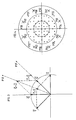
- the transcoding means 7 develop the control signals SCji1, SCji2 of the modulation cells CMi according to the constellation which it is desired to use for the modulation protocol. If the input signals SDi are 45 ° out of phase with each other (by the distribution line 8) and formed vectors respectively I U Q V as shown in Figure 3, the transcoding means 7 can be arranged according to the logic table below to address the 16 points P 31 to P 38; P 41 to P 48 of the larger amplitude constellation shown in FIG. 4. A circuit with 16 phase states (16-PSK) is then obtained in an extremely simple and reliable manner.
- Modulation signal Control signals Branch exit signals Points AT B VS D SCj11 SCj12 Scj21 SCj22 SCj31 SCj32 SCj41 SCj42 ss1 ss2 ss3 ss4 0 0 0 0 0 0 1 0 1 0 1 I U Q V P41 0 0 1 0 1 0 1 0 1 0 1 -I U Q V P42 0 1 0 0 1 0 1 0 1 0 1 0 1 -I -U Q V P43 0 1 1 0 1 0 1 0 1 0 1 0 1 0 1 0 1 0 1 0 1 -I -U -Q V P44 1 0 0 0 0 1 0 1 0 1 0 1 0 1 0 1 0 -I -U -Q -V P45 1 0 1 0 0 1 1 0 1 0 1 0 1 0 I -U -Q -V P46 1 1
- Points P41 to P48 are those traditionally obtained when the control signals SCji1, SCji2 are complementary. Dots P31 to P38 are obtained with identical control signals on one of the branches. Figure 3 illustrates the example of vector construction of points P31 and P41.
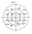
- FIG. 5 an example of a constellation has been represented. formed of 16 points A1, A2, A3, A4, A5, A6, A7, A8, A9, A10, A11, A12, A13, A14, A15, A16, allowing to achieve a 16-QAM modulation with a acceptable accuracy.
- the couple (0, 0) is used and not the couple (1, 1) capable of generating greater technological drifts.
- the invention can be the subject of numerous variants of realization with respect to the nonlimiting examples described above and represented.
- the modulation signal SCj is generally at a frequency lower than that ( ⁇ e / 2 ⁇ ) of the carrier signal.
- the frequency of the modulation signal SCj can be of the order of 100 MHz.
Landscapes
- Physics & Mathematics (AREA)
- Electromagnetism (AREA)
- Engineering & Computer Science (AREA)
- Computer Networks & Wireless Communication (AREA)
- Signal Processing (AREA)
- Digital Transmission Methods That Use Modulated Carrier Waves (AREA)
- Amplitude Modulation (AREA)
- Transmitters (AREA)
Claims (18)
- Verfahren zum Modulieren eines periodischen Trägersignals (Se) mit einem digitalen Modulationssignal (SCj), ausgeführt mit einer Modulatorschaltung (1), die wenigstens eine Modulationszelle (CMi) zum Empfangen von zwei digitalen Steuersignalen (SCji1, SCji2) umfasst, die gleich 0 oder 1 sein können und die für wenigstens einen Teil des digitalen Modulationssignals (SCj) repräsentativ sind, bei dem für wenigstens einen Wert des digitalen Modulationssignals (SCj) an wenigstens eine selbe Modulationszelle (CMi) zwei digitale Steuersignale (SCji1, SCji2) mit demselben Wert angelegt werden und für wenigstens einen anderen Wert des digitalen Modulationssignals (SCj) an diese Modulationszelle(n) (CMi) zwei digitale Steuersignale (SCji1, SCji2) mit komplementären Werten angelegt werden.
- Verfahren nach Anspruch 1, dadurch gekennzeichnet, dass wenigstens eine Modulationszelle (CMi), die zwei digitale Steuersignale (SCji1, SCji2) desselben Wertes für wenigstens einen Wert des digitalen Modulationssignals (SCj) empfängt, die Aufgabe hat, ein Signal zu erzeugen, moduliertes Grundsignal (Ssi) genannt, das für diesen Wert des digitalen Modulationssignals (SCj) null ist.
- Verfahren nach Anspruch 1 oder 2, dadurch gekennzeichnet, dass wenigstens eine Modulationszelle (CMi) eine durch Phasenverschiebung modulierte Zelle ist.
- Verfahren nach einem der Ansprüche 1 bis 3, dadurch gekennzeichnet, dass wenigstens eine Modulationszelle (CMi) die Aufgabe hat, ein moduliertes Grundsignal (Ssi) mit zwei einander entgegengesetzten Phasenzuständen und einem einzigen Amplitudenzustand zu erzeugen, wenn sie komplementäre digitale Steuersignale (SCji1, SCji2) erhält, und ein moduliertes Grundsignal (Ssi) zu erzeugen, das null ist, wenn es digitale Steuersignale (SCji1, SCji2) desselben Wertes erhält.
- Verfahren nach Anspruch 4, dadurch gekennzeichnet, dass, wenn die beiden digitalen Steuersignale (SCji1, SCji2) denselben Wert haben, beide gleich 0 sind.
- Verfahren nach einem der Ansprüche 1 bis 5, dadurch gekennzeichnet, dass die Modulatorschaltung (1) wenigstens zwei Modulationszellen (CMi) umfasst, und dadurch, dass für wenigstens einen Wert des digitalen Modulationssignals (SCj) an wenigstens eine Modulationszelle (CMi) zwei digitale Steuersignale (SCji1, SCji2) desselben Wertes angelegt werden und an wenigstens eine andere Modulationszelle (CMi) zwei digitale Steuersignale (SCji1, SCji2) mit komplementären Werten angelegt werden.
- Verfahren nach einem der Ansprüche 1 bis 6, dadurch gekennzeichnet, dass ein auf dem Trägersignal (Se) basierendes Eingangssignal (SDi) zu jeder Modulationszelle (CMi) mit Hilfe von Impedanzanpassungsmitteln (2) gesendet wird, die so gestaltet sind, dass die Impedanz der Modulationszelle (CMi) wenigstens im Wesentlichen gleich gut angepasst ist, wenn die digitalen Steuersignale (SCji1, SCji2), die sie empfängt, komplementär sind wie wenn sie gleich sind.
- Verfahren nach Anspruch 7, dadurch gekennzeichnet, dass die Impedanzanpassungsmittel (2) für jede Modulationszelle (CMi) einen Transistor (3), der das Eingangssignal (SDi) empfängt und mit der Modulationszelle (CMi) verbunden ist, und einen parallelen Widerstand (6) zwischen dem Transistor (3) und Masse umfasst.
- Verfahren nach einem der Ansprüche 1 bis 8, dadurch gekennzeichnet, dass eine Modulatorschaltung (1) mit verteilter Struktur verwendet wird, die mehrere abgeleitete Zweige (Bi) umfasst, die jeweils wenigstens eine Modulationszelle (CMi) zum Empfangen von zwei digitalen Steuersignalen (SCji1, SCji2) umfassen, wobei jeder abgeleitete Zweig (Bi) ein Signal liefert, moduliertes Zweigausgangssignal (Ssi) genannt, und dadurch, dass die modulierten Zweigausgangssignale (Ssi) von den verschiedenen abgeleiteten Zweigen (Bi) phasensummiert werden, um ein moduliertes Ausgangssignal (Ss) zu bilden.
- Modulatorschaltung zum Durchführen der Modulation eines periodischen Trägersignals (Se) mit einem digitalen Modulationssignal (SCj), die wenigstens eine Modulationszelle (CMi) zum Empfangen von zwei digitalen Steuersignalen (SCji1, SCji2) umfasst, die gleich 0 oder 1 sein können und die für wenigstens einen Teil des digitalen Modulationssignals (SCj) repräsentativ sind, wobei diese Schaltung so gestaltet ist, dass für wenigstens einen Wert des digitalen Modulationssignals (SCj) wenigstens eine selbe Modulationszelle (CMi) zwei digitale Steuersignale (SCji1, SCji2) desselben Wertes erhält, und dass für wenigstens einen anderen Wert des digitalen Modulationssignals (SCj) diese Modulationszelle(n) (CMi) zwei digitale Steuersignale (SCji1, SCji2) mit komplementären Werten erhält/erhalten.
- Schaltung nach Anspruch 10, dadurch gekennzeichnet, dass wenigstens eine Modulationszelle (CMi), die zwei digitale Steuersignale (SCji1, SCji2) desselben Wertes für wenigstens einen Wert des digitalen Modulationssignals (SCj) empfängt, die Aufgabe hat, ein Signal zu erzeugen, moduliertes Grundsignal (Ssi) genannt, das für diesen Wert des digitalen Modulationssignals (SCj) null ist.
- Schaltung nach Anspruch 10 oder 11, dadurch gekennzeichnet, dass wenigstens eine Modulationszelle (CMi) eine durch Phasenverschiebung modulierte Zelle ist.
- Schaltung nach einem der Ansprüche 10 bis 12, dadurch gekennzeichnet, dass wenigstens eine Modulationszelle (CMi) die Aufgabe hat, ein moduliertes Grundsignal (Ssi) mit zwei einander entgegengesetzten Phasenzuständen und einem einzigen Amplitudenzustand zu erzeugen, wenn sie komplementäre digitale Steuersignale (SCji1, SCji2) erhält, und ein moduliertes Grundsignal (Ssi) zu erzeugen, das null ist, wenn es digitale Steuersignale (SCji1, SCji2) desselben Wertes erhält.
- Schaltung nach Anspruch 13, dadurch gekennzeichnet, dass, wenn die beiden digitalen Steuersignale (SCji1, SCji2) denselben Wert haben, beide gleich 0 sind.
- Schaltung nach einem der Ansprüche 10 bis 14, dadurch gekennzeichnet, dass sie wenigstens zwei Modulationszellen (CMi) umfasst, und dadurch, dass sie so gestaltet ist, dass für wenigstens einen Wert des digitalen Modulationssignals (SCj) wenigstens eine Modulationszelle (CMi) zwei digitale Steuersignale (SCji1, SCji2) desselben Wertes erhält und wenigstens eine andere Modulationszelle (CMi) zwei digitale Steuersignale (SCji1, SCji2) mit komplementären Werten erhält/erhalten.
- Schaltung nach einem der Ansprüche 10 bis 15, dadurch gekennzeichnet, dass sie jeder Modulationszelle (CMi) vorgeschaltet Impedanzanpassungsmittel (2) umfasst, die ein auf dem Trägersignal (Se) basierendes Eingangssignal (SDi) zu jeder Modulationszelle (CMi) senden und so gestaltet sind, dass die Impedanz der Modulationszelle (CMi) wenigstens im Wesentlichen genauso gut angepasst ist, wenn die digitalen Steuersignale (SCji1, SCji2), die sie empfängt, komplementär sind wie wenn sie gleich sind.
- Schaltung nach Anspruch 16, dadurch gekennzeichnet, dass die Impedanzanpassungsmittel (2) für jede Modulationszelle (CMi) einen Transistor (3), der das Eingangssignal (SDi) empfängt und mit der Modulationszelle (CMi) verbunden ist, und einen parallelen Widerstand (6) zwischen dem Transistor (3) und Masse umfasst.
- Schaltung nach einem der Ansprüche 10 bis 17, dadurch gekennzeichnet, dass sie eine verteilte Struktur aufweist, die mehrere abgeleitete Zweige (Bi), die jeweils Folgendes umfassen: wenigstens eine Modulationszelle (CMi) zum Empfangen von zwei digitalen Steuersignalen (SCji1, SCji2) umfassen, wobei jeder abgeleitete Zweig (Bi) ein Signal liefert, moduliertes Zweigausgangssignal (Ssi) genannt, und Mittel (12) zum Phasensummieren der modulierten Zweigausgangssignale (Ssi) von den verschiedenen abgeleiteten Zweigen (Bi), um ein moduliertes Ausgangssignal (Ss) zu bilden.
Applications Claiming Priority (3)
| Application Number | Priority Date | Filing Date | Title |
|---|---|---|---|
| FR0009241A FR2811826B1 (fr) | 2000-07-13 | 2000-07-13 | Procede et circuit de modulation numerique a composantes du signal de sortie module pouvant etre nulles |
| FR0009241 | 2000-07-13 | ||
| PCT/FR2001/002199 WO2002007303A1 (fr) | 2000-07-13 | 2001-07-09 | Circulation de modulation numerique de phase et amplitude et procede |
Publications (2)
| Publication Number | Publication Date |
|---|---|
| EP1316142A1 EP1316142A1 (de) | 2003-06-04 |
| EP1316142B1 true EP1316142B1 (de) | 2004-04-07 |
Family
ID=8852503
Family Applications (1)
| Application Number | Title | Priority Date | Filing Date |
|---|---|---|---|
| EP01984282A Expired - Lifetime EP1316142B1 (de) | 2000-07-13 | 2001-07-09 | Digitaler phasen- und amplitudenmodulator, und verfahren dazu |
Country Status (8)
| Country | Link |
|---|---|
| US (1) | US6831526B2 (de) |
| EP (1) | EP1316142B1 (de) |
| JP (1) | JP4803695B2 (de) |
| AT (1) | ATE264019T1 (de) |
| DE (1) | DE60102709T2 (de) |
| ES (1) | ES2219576T3 (de) |
| FR (1) | FR2811826B1 (de) |
| WO (1) | WO2002007303A1 (de) |
Families Citing this family (17)
| Publication number | Priority date | Publication date | Assignee | Title |
|---|---|---|---|---|
| US7138882B2 (en) | 2002-11-08 | 2006-11-21 | Northrop Grumman Corp | Architecture for universal modulator |
| US7742812B2 (en) | 2006-03-29 | 2010-06-22 | Medtronic, Inc. | Method and apparatus for detecting arrhythmias in a medical device |
| US8874987B2 (en) * | 2011-10-06 | 2014-10-28 | Nec Laboratories America, Inc. | Optimum signal constellation design for high-speed optical transmission |
| CN105264773B (zh) * | 2013-03-15 | 2018-02-09 | Tm Ip 控股有限公司 | 易位调制系统和方法 |
| US9775559B2 (en) | 2013-04-26 | 2017-10-03 | Medtronic, Inc. | Staged rhythm detection system and method |
| US10376705B2 (en) | 2014-04-01 | 2019-08-13 | Medtronic, Inc. | Method and apparatus for discriminating tachycardia events in a medical device |
| US9526908B2 (en) | 2014-04-01 | 2016-12-27 | Medtronic, Inc. | Method and apparatus for discriminating tachycardia events in a medical device |
| US9808640B2 (en) | 2014-04-10 | 2017-11-07 | Medtronic, Inc. | Method and apparatus for discriminating tachycardia events in a medical device using two sensing vectors |
| US9352165B2 (en) | 2014-04-17 | 2016-05-31 | Medtronic, Inc. | Method and apparatus for verifying discriminating of tachycardia events in a medical device having dual sensing vectors |
| US10278601B2 (en) | 2014-04-24 | 2019-05-07 | Medtronic, Inc. | Method and apparatus for selecting a sensing vector configuration in a medical device |
| US10244957B2 (en) | 2014-04-24 | 2019-04-02 | Medtronic, Inc. | Method and apparatus for selecting a sensing vector configuration in a medical device |
| US9795312B2 (en) | 2014-04-24 | 2017-10-24 | Medtronic, Inc. | Method and apparatus for adjusting a blanking period for selecting a sensing vector configuration in a medical device |
| US10252067B2 (en) | 2014-04-24 | 2019-04-09 | Medtronic, Inc. | Method and apparatus for adjusting a blanking period during transitioning between operating states in a medical device |
| US9610025B2 (en) | 2014-07-01 | 2017-04-04 | Medtronic, Inc. | Method and apparatus for verifying discriminating of tachycardia events in a medical device having dual sensing vectors |
| US10188867B2 (en) | 2015-01-23 | 2019-01-29 | Medtronic, Inc. | Method and apparatus for beat acquisition during template generation in a medical device having dual sensing vectors |
| US9561005B2 (en) | 2015-01-23 | 2017-02-07 | Medtronic, Inc. | Method and apparatus for beat acquisition during template generation in a medical device having dual sensing vectors |
| CN115208421B (zh) * | 2022-07-25 | 2024-11-05 | 上海航天测控通信研究所 | 一种宇航器调幅发射机电路 |
Family Cites Families (9)
| Publication number | Priority date | Publication date | Assignee | Title |
|---|---|---|---|---|
| US3867574A (en) * | 1973-06-20 | 1975-02-18 | Gen Motors Corp | Three phase jump encoder and decoder |
| US4994773A (en) * | 1988-10-13 | 1991-02-19 | Chen Tzu H | Digitally controlled monolithic active phase shifter apparatus having a cascode configuration |
| US5063361A (en) * | 1990-12-21 | 1991-11-05 | Raytheon Company | Serrodyne modulator |
| US5237292A (en) * | 1992-07-01 | 1993-08-17 | Space Systems/Loral | Quadrature amplitude modulation system with compensation for transmission system characteristics |
| US5442327A (en) * | 1994-06-21 | 1995-08-15 | Motorola, Inc. | MMIC tunable biphase modulator |
| US5463355A (en) * | 1994-07-15 | 1995-10-31 | Loral Aerospace Corp. | Wideband vector modulator which combines outputs of a plurality of QPSK modulators |
| US5428320A (en) | 1994-08-29 | 1995-06-27 | Motorola, Inc. | Biphase modulator and method without matching elements |
| FR2760301B1 (fr) * | 1997-02-28 | 1999-04-30 | Centre Nat Etd Spatiales | Circuit electronique modulateur par deplacement de phase a structure distribuee |
| US6201452B1 (en) * | 1998-12-10 | 2001-03-13 | Ericsson Inc. | Systems and methods for converting a stream of complex numbers into a modulated radio power signal |
-
2000
- 2000-07-13 FR FR0009241A patent/FR2811826B1/fr not_active Expired - Fee Related
-
2001
- 2001-07-09 JP JP2002513084A patent/JP4803695B2/ja not_active Expired - Fee Related
- 2001-07-09 DE DE60102709T patent/DE60102709T2/de not_active Expired - Lifetime
- 2001-07-09 WO PCT/FR2001/002199 patent/WO2002007303A1/fr not_active Ceased
- 2001-07-09 EP EP01984282A patent/EP1316142B1/de not_active Expired - Lifetime
- 2001-07-09 AT AT01984282T patent/ATE264019T1/de not_active IP Right Cessation
- 2001-07-09 US US10/332,458 patent/US6831526B2/en not_active Expired - Lifetime
- 2001-07-09 ES ES01984282T patent/ES2219576T3/es not_active Expired - Lifetime
Also Published As
| Publication number | Publication date |
|---|---|
| ATE264019T1 (de) | 2004-04-15 |
| US20040021523A1 (en) | 2004-02-05 |
| FR2811826B1 (fr) | 2002-10-11 |
| WO2002007303A8 (fr) | 2002-04-04 |
| ES2219576T3 (es) | 2004-12-01 |
| EP1316142A1 (de) | 2003-06-04 |
| DE60102709T2 (de) | 2005-03-17 |
| JP2004504748A (ja) | 2004-02-12 |
| JP4803695B2 (ja) | 2011-10-26 |
| DE60102709D1 (de) | 2004-05-13 |
| WO2002007303A1 (fr) | 2002-01-24 |
| FR2811826A1 (fr) | 2002-01-18 |
| US6831526B2 (en) | 2004-12-14 |
Similar Documents
| Publication | Publication Date | Title |
|---|---|---|
| EP1316142B1 (de) | Digitaler phasen- und amplitudenmodulator, und verfahren dazu | |
| EP1214780B1 (de) | Sender für funksignale, die mit einer autoadaptiven verstärkerspolarisation moduliert werden | |
| EP3528391B1 (de) | Nfc steureinheit | |
| FR2798244A1 (fr) | Circuit et procede d'amplification de puissance a rendement eleve autorisant une large gamme de reduction de puissance dynamique | |
| FR2696295A1 (fr) | Dispositif pour corriger les distorsions non-linéaires d'un amplificateur électronique. | |
| FR2709217A1 (fr) | Procédé et dispositif d'adaptation d'impédance pour un émetteur et/ou récepteur, circuit intégré et système de transmission les mettant en Óoeuvre. | |
| EP0795957B1 (de) | Vorrichtung mit einer passiven um 180 Grad phasenverschiebenden Kopplungsschaltung | |
| FR2543379A1 (fr) | Dispositif de demodulation directe en hyperfrequence et chaine de reception hyperfrequence comportant un tel dispositif | |
| EP0487386A1 (de) | Frequenzvervielfacher | |
| FR2721156A1 (fr) | Circuit de linéarisation à prédistorsion. | |
| FR3026250A1 (fr) | Dispositif electronique pour une chaine de reception de signaux radiofrequence, comprenant un etage amplificateur transconducteur a faible bruit | |
| FR2545295A1 (fr) | Amplificateur hyperfrequence de puissance | |
| FR2969426A1 (fr) | Circuit de dephasage | |
| FR2666186A1 (fr) | Duplexeur bidirectionnel pour ondes hyperfrequences polarisees realisable notamment en technologie monolithique sur arseniure de gallium. | |
| EP1652293A1 (de) | Verstärker mit grosser ausgangsleistungsdynamik | |
| EP0963623B1 (de) | Elektronische phasenumtastung-modulatorschaltung mit verteilter struktur | |
| EP0195709B1 (de) | Digitaler Wellenformgenerator und zugehöriges Verfahren | |
| EP0645884B1 (de) | Verstärkerkette in Strommode, Operationsverstärker, Verstärkungszelle und zugehöriges Verstärkerelement | |
| EP3824549A1 (de) | Architektur für hf-funkfrequenzsender | |
| EP0032332A1 (de) | Hochfrequenzleistungsteiler und Hochfrequenzschaltungen, insbesondere Halbleiterschaltungen mit einem solchen Teiler | |
| FR2525834A1 (fr) | Amplificateur de puissance a haute frequence a puissance de sortie commutable rapidement par paliers | |
| EP1017171B1 (de) | Phasensteuervorrichtung mit einer Vielzahl von Kettenverstärkerstrukturen mit schaltbaren aktiven Elementen zur Erstellung einer Übertragungsleitung mit programmierbarer Länge | |
| EP0347985A1 (de) | Allpasstyp-Schaltung für ultrahohe Frequenzen | |
| FR2609585A1 (fr) | Circuit realisant la fonction ou-exclusif | |
| WO2000039918A1 (fr) | Procede de modulation analogique et circuit integre monolithique a etage melangeur comprenant des transistors a effet de champ non polarises |
Legal Events
| Date | Code | Title | Description |
|---|---|---|---|
| PUAI | Public reference made under article 153(3) epc to a published international application that has entered the european phase |
Free format text: ORIGINAL CODE: 0009012 |
|
| 17P | Request for examination filed |
Effective date: 20030110 |
|
| AK | Designated contracting states |
Designated state(s): AT BE CH CY DE DK ES FI FR GB GR IE IT LI LU MC NL PT SE TR |
|
| GRAP | Despatch of communication of intention to grant a patent |
Free format text: ORIGINAL CODE: EPIDOSNIGR1 |
|
| GRAS | Grant fee paid |
Free format text: ORIGINAL CODE: EPIDOSNIGR3 |
|
| GRAA | (expected) grant |
Free format text: ORIGINAL CODE: 0009210 |
|
| AK | Designated contracting states |
Kind code of ref document: B1 Designated state(s): AT BE CH CY DE DK ES FI FR GB GR IE IT LI LU MC NL PT SE TR |
|
| PG25 | Lapsed in a contracting state [announced via postgrant information from national office to epo] |
Ref country code: CY Free format text: LAPSE BECAUSE OF FAILURE TO SUBMIT A TRANSLATION OF THE DESCRIPTION OR TO PAY THE FEE WITHIN THE PRESCRIBED TIME-LIMIT Effective date: 20040407 Ref country code: TR Free format text: LAPSE BECAUSE OF FAILURE TO SUBMIT A TRANSLATION OF THE DESCRIPTION OR TO PAY THE FEE WITHIN THE PRESCRIBED TIME-LIMIT Effective date: 20040407 Ref country code: NL Free format text: LAPSE BECAUSE OF FAILURE TO SUBMIT A TRANSLATION OF THE DESCRIPTION OR TO PAY THE FEE WITHIN THE PRESCRIBED TIME-LIMIT Effective date: 20040407 Ref country code: FI Free format text: LAPSE BECAUSE OF FAILURE TO SUBMIT A TRANSLATION OF THE DESCRIPTION OR TO PAY THE FEE WITHIN THE PRESCRIBED TIME-LIMIT Effective date: 20040407 Ref country code: AT Free format text: LAPSE BECAUSE OF FAILURE TO SUBMIT A TRANSLATION OF THE DESCRIPTION OR TO PAY THE FEE WITHIN THE PRESCRIBED TIME-LIMIT Effective date: 20040407 Ref country code: IE Free format text: LAPSE BECAUSE OF FAILURE TO SUBMIT A TRANSLATION OF THE DESCRIPTION OR TO PAY THE FEE WITHIN THE PRESCRIBED TIME-LIMIT Effective date: 20040407 |
|
| REG | Reference to a national code |
Ref country code: GB Ref legal event code: FG4D Free format text: NOT ENGLISH |
|
| REG | Reference to a national code |
Ref country code: CH Ref legal event code: EP |
|
| REF | Corresponds to: |
Ref document number: 60102709 Country of ref document: DE Date of ref document: 20040513 Kind code of ref document: P |
|
| REG | Reference to a national code |
Ref country code: IE Ref legal event code: FG4D Free format text: FRENCH |
|
| PG25 | Lapsed in a contracting state [announced via postgrant information from national office to epo] |
Ref country code: GR Free format text: LAPSE BECAUSE OF FAILURE TO SUBMIT A TRANSLATION OF THE DESCRIPTION OR TO PAY THE FEE WITHIN THE PRESCRIBED TIME-LIMIT Effective date: 20040707 Ref country code: DK Free format text: LAPSE BECAUSE OF FAILURE TO SUBMIT A TRANSLATION OF THE DESCRIPTION OR TO PAY THE FEE WITHIN THE PRESCRIBED TIME-LIMIT Effective date: 20040707 Ref country code: SE Free format text: LAPSE BECAUSE OF FAILURE TO SUBMIT A TRANSLATION OF THE DESCRIPTION OR TO PAY THE FEE WITHIN THE PRESCRIBED TIME-LIMIT Effective date: 20040707 |
|
| PG25 | Lapsed in a contracting state [announced via postgrant information from national office to epo] |
Ref country code: LU Free format text: LAPSE BECAUSE OF NON-PAYMENT OF DUE FEES Effective date: 20040709 |
|
| PG25 | Lapsed in a contracting state [announced via postgrant information from national office to epo] |
Ref country code: MC Free format text: LAPSE BECAUSE OF NON-PAYMENT OF DUE FEES Effective date: 20040731 Ref country code: BE Free format text: LAPSE BECAUSE OF NON-PAYMENT OF DUE FEES Effective date: 20040731 |
|
| GBT | Gb: translation of ep patent filed (gb section 77(6)(a)/1977) |
Effective date: 20040729 |
|
| NLV1 | Nl: lapsed or annulled due to failure to fulfill the requirements of art. 29p and 29m of the patents act | ||
| REG | Reference to a national code |
Ref country code: IE Ref legal event code: FD4D Ref country code: ES Ref legal event code: FG2A Ref document number: 2219576 Country of ref document: ES Kind code of ref document: T3 |
|
| BERE | Be: lapsed |
Owner name: CENTRE NATIONAL D'ETUDES *SPATIALES Effective date: 20040731 |
|
| PLBE | No opposition filed within time limit |
Free format text: ORIGINAL CODE: 0009261 |
|
| STAA | Information on the status of an ep patent application or granted ep patent |
Free format text: STATUS: NO OPPOSITION FILED WITHIN TIME LIMIT |
|
| 26N | No opposition filed |
Effective date: 20050110 |
|
| PG25 | Lapsed in a contracting state [announced via postgrant information from national office to epo] |
Ref country code: LI Free format text: LAPSE BECAUSE OF NON-PAYMENT OF DUE FEES Effective date: 20050731 Ref country code: CH Free format text: LAPSE BECAUSE OF NON-PAYMENT OF DUE FEES Effective date: 20050731 |
|
| REG | Reference to a national code |
Ref country code: CH Ref legal event code: PL |
|
| BERE | Be: lapsed |
Owner name: CENTRE NATIONAL D'ETUDES *SPATIALES Effective date: 20040731 |
|
| PG25 | Lapsed in a contracting state [announced via postgrant information from national office to epo] |
Ref country code: PT Free format text: LAPSE BECAUSE OF NON-PAYMENT OF DUE FEES Effective date: 20040907 |
|
| REG | Reference to a national code |
Ref country code: FR Ref legal event code: PLFP Year of fee payment: 16 |
|
| PGFP | Annual fee paid to national office [announced via postgrant information from national office to epo] |
Ref country code: GB Payment date: 20160719 Year of fee payment: 16 Ref country code: DE Payment date: 20160719 Year of fee payment: 16 Ref country code: IT Payment date: 20160725 Year of fee payment: 16 |
|
| PGFP | Annual fee paid to national office [announced via postgrant information from national office to epo] |
Ref country code: FR Payment date: 20160729 Year of fee payment: 16 |
|
| PGFP | Annual fee paid to national office [announced via postgrant information from national office to epo] |
Ref country code: ES Payment date: 20160729 Year of fee payment: 16 |
|
| REG | Reference to a national code |
Ref country code: DE Ref legal event code: R119 Ref document number: 60102709 Country of ref document: DE |
|
| GBPC | Gb: european patent ceased through non-payment of renewal fee |
Effective date: 20170709 |
|
| REG | Reference to a national code |
Ref country code: FR Ref legal event code: ST Effective date: 20180330 |
|
| PG25 | Lapsed in a contracting state [announced via postgrant information from national office to epo] |
Ref country code: DE Free format text: LAPSE BECAUSE OF NON-PAYMENT OF DUE FEES Effective date: 20180201 Ref country code: GB Free format text: LAPSE BECAUSE OF NON-PAYMENT OF DUE FEES Effective date: 20170709 |
|
| PG25 | Lapsed in a contracting state [announced via postgrant information from national office to epo] |
Ref country code: FR Free format text: LAPSE BECAUSE OF NON-PAYMENT OF DUE FEES Effective date: 20170731 |
|
| PG25 | Lapsed in a contracting state [announced via postgrant information from national office to epo] |
Ref country code: IT Free format text: LAPSE BECAUSE OF NON-PAYMENT OF DUE FEES Effective date: 20170709 |
|
| REG | Reference to a national code |
Ref country code: ES Ref legal event code: FD2A Effective date: 20181030 |
|
| PG25 | Lapsed in a contracting state [announced via postgrant information from national office to epo] |
Ref country code: ES Free format text: LAPSE BECAUSE OF NON-PAYMENT OF DUE FEES Effective date: 20170710 |