EP1315183A2 - Winding for a transformer or a coil - Google Patents
Winding for a transformer or a coil Download PDFInfo
- Publication number
- EP1315183A2 EP1315183A2 EP02024178A EP02024178A EP1315183A2 EP 1315183 A2 EP1315183 A2 EP 1315183A2 EP 02024178 A EP02024178 A EP 02024178A EP 02024178 A EP02024178 A EP 02024178A EP 1315183 A2 EP1315183 A2 EP 1315183A2
- Authority
- EP
- European Patent Office
- Prior art keywords
- winding
- layer
- insulating
- insulating layer
- thickness
- Prior art date
- Legal status (The legal status is an assumption and is not a legal conclusion. Google has not performed a legal analysis and makes no representation as to the accuracy of the status listed.)
- Granted
Links
Images

Classifications
-
- H—ELECTRICITY
- H01—ELECTRIC ELEMENTS
- H01F—MAGNETS; INDUCTANCES; TRANSFORMERS; SELECTION OF MATERIALS FOR THEIR MAGNETIC PROPERTIES
- H01F27/00—Details of transformers or inductances, in general
- H01F27/28—Coils; Windings; Conductive connections
- H01F27/30—Fastening or clamping coils, windings, or parts thereof together; Fastening or mounting coils or windings on core, casing, or other support
-
- H—ELECTRICITY
- H01—ELECTRIC ELEMENTS
- H01F—MAGNETS; INDUCTANCES; TRANSFORMERS; SELECTION OF MATERIALS FOR THEIR MAGNETIC PROPERTIES
- H01F27/00—Details of transformers or inductances, in general
- H01F27/28—Coils; Windings; Conductive connections
- H01F27/2847—Sheets; Strips
-
- H—ELECTRICITY
- H01—ELECTRIC ELEMENTS
- H01F—MAGNETS; INDUCTANCES; TRANSFORMERS; SELECTION OF MATERIALS FOR THEIR MAGNETIC PROPERTIES
- H01F27/00—Details of transformers or inductances, in general
- H01F27/28—Coils; Windings; Conductive connections
- H01F27/32—Insulating of coils, windings, or parts thereof
- H01F27/323—Insulation between winding turns, between winding layers
-
- Y—GENERAL TAGGING OF NEW TECHNOLOGICAL DEVELOPMENTS; GENERAL TAGGING OF CROSS-SECTIONAL TECHNOLOGIES SPANNING OVER SEVERAL SECTIONS OF THE IPC; TECHNICAL SUBJECTS COVERED BY FORMER USPC CROSS-REFERENCE ART COLLECTIONS [XRACs] AND DIGESTS
- Y10—TECHNICAL SUBJECTS COVERED BY FORMER USPC
- Y10T—TECHNICAL SUBJECTS COVERED BY FORMER US CLASSIFICATION
- Y10T29/00—Metal working
- Y10T29/49—Method of mechanical manufacture
- Y10T29/49002—Electrical device making
- Y10T29/4902—Electromagnet, transformer or inductor
Definitions
- the invention relates to a winding for a transformer or a coil with a band-shaped electrical conductor and with an insulating material layer of band-shaped Insulation material that winds together around a winding core are wound, the individual turns of the winding a predetermined Have winding angles with respect to the winding axis of the winding core and are arranged with each other with partial overlap, and wherein between an insulating layer is interposed between two radially adjacent layers of turns is.
- the turns are usually wrapped close together in the axial direction and at least one Layer formed by turns.
- the object of the invention is characterized in that the local voltage differences or a voltage difference curve between the two relevant radially adjacent layers in the direction of Winding axis is determined and that the thickness of the insulating layer locally to each voltage difference determined there is adapted.
- the insulation layer is therefore not in accordance the previously known prior art with an equally large layer thickness designed, but the thickness is related to the voltage difference between the adapted radially adjacent rows. Accordingly, the axial Places where the voltage difference is comparatively small, insulation material be saved. This also ensures that the transformer or the coil overall has a comparatively better surge voltage resistance between the layers.
- An advantageous embodiment of the subject matter of the invention is that at the arrangement of two radially adjacent insulating layers the calculated total thickness these two insulating layers are approximately the same at each axial location Has thickness.
- the first layer 18 of windings is the layer that is directly around the winding core 10 is wound.
- the band-shaped insulation material 16 is included arranged such that it lies between the winding core 10 and the conductor 14.
- the individual turns of the first layer 18 are at a certain angle 20 inclined with respect to the winding axis 12.
- each turn is one certain amount parallel to the direction of the winding axis 12 compared to the previous one Winding arranged offset, such that a next following winding has a partial overlap with the previous turn.
- a second layer 22 of turns is wound radially around the first layer 18.
- an insulation material of a certain width with a predefinable one Feed can be wound continuously. It is not essential necessary that at the first, i.e. thinnest stage, a closed one Layer arises, d. H. the feed can be larger than the width of the winding Material, if the inserted winding insulation is already used for the insulation sufficient between two layers.
- the winding insulation is particularly that tape-shaped insulation material layer, which is applied to the electrical conductor or is placed on the conductor as a strip material or as a film. Will the If the feed is halved, there is an insulating layer of double thickness. In this way a step-like isolation can also be achieved without the isolation process must be interrupted in the meantime.
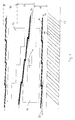
- FIG. 2 shows a first insulating wedge 40 opposite a second insulating wedge 42 lies and which are used in principle as the first 26 or second insulating layer 32 could.
- first insulating wedge 40 opposite a second insulating wedge 42 lies and which are used in principle as the first 26 or second insulating layer 32 could.
- first 26 or second insulating layer 32 could be used in principle as the first 26 or second insulating layer 32 could.
- only the basic structure and the effect of Arrangement of two insulating wedges 40, 42 are shown.
- the dimensions or the proportions in this figure are not to scale and also not the representation comparable to Fig. 1.
Landscapes
- Engineering & Computer Science (AREA)
- Power Engineering (AREA)
- Coils Of Transformers For General Uses (AREA)
- Insulating Of Coils (AREA)
- Transformers For Measuring Instruments (AREA)
Abstract
Description
Die Erfindung betrifft eine Wicklung für einen Transformator oder eine Spule mit einem bandförmigen elektrischen Leiter und mit einer Isoliermaterialschicht aus bandförmigen Isolationsmaterial, die gemeinsam zu Windungen um einen Wicklungskern gewickelt sind, wobei die einzelnen Windungen der Wicklung einen vorgegebenen Wicklungswinkel gegenüber der Wicklungsachse des Wicklungskerns aufweisen und zueinander mit teilweiser Überlappung angeordnet sind, und wobei zwischen zwei radial benachbarten Lagen von Windungen eine Isolierschicht zwischengefügt ist.The invention relates to a winding for a transformer or a coil with a band-shaped electrical conductor and with an insulating material layer of band-shaped Insulation material that winds together around a winding core are wound, the individual turns of the winding a predetermined Have winding angles with respect to the winding axis of the winding core and are arranged with each other with partial overlap, and wherein between an insulating layer is interposed between two radially adjacent layers of turns is.
Bei derartigen, allgemein bekannten Wicklungen werden die Windungen üblicherweise in axialer Richtung dicht nebeneinander liegend gewickelt und wenigstens eine Lage von Windungen gebildet.In such well-known windings, the turns are usually wrapped close together in the axial direction and at least one Layer formed by turns.
Häufig werden aber auch mehrere Lagen radial aneinander gefügt und bilden einen mehrlagigen Transformator oder eine mehrlagige Spule. Im Falle von mehreren Lagen von Windungen ist häufig zwischen zwei benachbarten Lagen jeweils eine Isolierschicht ein- beziehungsweise zwischengefügt. Diese Isolierschicht verhindert Spannungsüberschläge zwischen den Lagen und ist demgemäß auf die größte vorkommende Spannungsdifferenz zwischen zwei Lagen ausgelegt. Frequently, however, several layers are joined together radially and form one multi-layer transformer or a multi-layer coil. In the case of several layers Of turns there is often an insulating layer between two adjacent layers inserted or interposed. This insulating layer prevents Voltage flashovers between the layers and is accordingly the largest occurring Voltage difference between two layers.
Ausgehend von diesem Stand der Technik ist es Aufgabe der Erfindung, eine Wicklung für einen Transformator oder eine Spule anzugeben, bei der lsolationsmater eingespart werden kann und bei der zugleich eine ausreichende Spannungsfestigkeit erreicht wird, insbesondere eine gute Stoßspannungsfestigkeit zwischen zwei radial benachbarten Lagen von Windungen.Starting from this prior art, it is an object of the invention to provide a winding to specify for a transformer or a coil at the insulation mat can be saved and at the same time sufficient voltage resistance is achieved, in particular a good surge voltage resistance between two radial adjacent layers of turns.
Die Aufgabe wird erfindungsgemäß gelöst durch eine Wicklung für einen Transformator oder eine Spule mit den in Anspruch 1 genannten Merkmalen.The object is achieved according to the invention by a winding for a transformer or a coil with the features mentioned in claim 1.
Demgemäß ist der erfindungsgemäße Gegenstand dadurch gekennzeichnet, daß die örtliche Spannungsdifferenzen beziehungsweise ein Spannungsdifferenzenverlauf zwischen den zwei betreffenden radial benachbarten Lagen in Richtung der Wicklungsachse ermittelt ist und daß die Dicke der Isolierschicht örtlich jeweils an die dort ermittelte Spannungsdifferenz angepaßt ist. Die Isolierschicht ist also nicht gemäß dem bisher bekannten Stand der Technik mit einer gleichgroßen Schichtdicke ausgestaltet, sondern die Dicke ist auf die Spannungsdifferenz zwischen den betreffenden radial benachbarten Reihen angepaßt. Dementsprechend kann an den axialen Stellen, an denen die Spannungsdifferenz vergleichsweise gering ist, Isolationsmaterial eingespart werden. Zudem wird hiermit erreicht, daß der Transformator bzw. die Spule insgesamt eine vergleichsweise bessere Stoßspannungsfestigkeit zwischen den Lagen aufweist.Accordingly, the object of the invention is characterized in that the local voltage differences or a voltage difference curve between the two relevant radially adjacent layers in the direction of Winding axis is determined and that the thickness of the insulating layer locally to each voltage difference determined there is adapted. The insulation layer is therefore not in accordance the previously known prior art with an equally large layer thickness designed, but the thickness is related to the voltage difference between the adapted radially adjacent rows. Accordingly, the axial Places where the voltage difference is comparatively small, insulation material be saved. This also ensures that the transformer or the coil overall has a comparatively better surge voltage resistance between the layers.
Eine vorteilhafte Ausgestaltung des Erfindungsgegenstands besteht darin, daß bei der Anordnung zweier radial benachbarter Isolierschichten die rechnerische Gesamtdicke dieser zwei Isolierschichten an jeder axialen Stelle in etwa die gleiche Dicke aufweist. Mit dieser Ausgestaltung wird vorteilhafterweise erreicht, daß die durch die unterschiedlichen Isolierschichtdicken resultierenden verschiedenen Außendurchmesser einer Lage durch das erfindungsgemäße Profil einer weiteren Isolierschicht zwischen der Lage und einer nächst folgenden Lage wieder ausgeglichen ist und derart ein insgesamt einheitlicher Außendurchmesser des Transformators bzw. der Spule erreicht ist. An advantageous embodiment of the subject matter of the invention is that at the arrangement of two radially adjacent insulating layers the calculated total thickness these two insulating layers are approximately the same at each axial location Has thickness. With this configuration it is advantageously achieved that the different outer diameters resulting from the different insulation layer thicknesses a layer through the profile of another insulating layer according to the invention balanced between the location and a next location is and such an overall uniform outer diameter of the transformer or the coil is reached.
Eine günstige Ausgestaltung des erfindungsgemäßen Gegenstandes sieht vor, daß die Dickenänderung der Isolierschicht in axialer Richtung kontinuierlich ausgestaltet ist. Auf diese Weise entsteht in etwa ein keilförmiges Profil der Isolierschicht, für den Fall, daß das Schnittbild durch die Wicklungsachse betrachtet wird. Es ist aber ohne weiteres denkbar, daß ein im Schnittbild sägezahnformiges oder wolliges Profil vorgesehen ist, beispielsweise dann, wenn zwei Spulen direkt nebeneinander angeordnet sind.A favorable embodiment of the object of the invention provides that the change in thickness of the insulating layer is designed continuously in the axial direction is. In this way, a wedge-shaped profile of the insulating layer is created for the Case that the sectional view is viewed through the winding axis. But it is without further conceivable that a sawtooth-shaped or woolly profile is provided in the sectional view is, for example, when two coils are arranged directly next to each other are.
Besonders vorteilhaft ist es jedoch, wenn die Dickenänderung der Isolierschicht in axialer Richtung stufenförmig ausgestaltet ist. Das heißt in axialer Richtung betrachtet, ändert sich die Dicke der Isolierschicht sprunghaft in Stufen, also diskontinuierlich, ohne das dies für die Spannungsfestigkeit nachteilig ist. Zudem kann die Produktion der Isolierschicht bei dieser Ausgestaltung wesentlich einfacher erfolgen und das üblicherweise bandförmige Isoliermaterial Lage für Lage zu der Isolierschicht gewickelt werden.However, it is particularly advantageous if the change in thickness of the insulating layer in axial direction is stepped. That is, viewed in the axial direction, the thickness of the insulating layer changes in steps, i.e. discontinuously, without this being disadvantageous for the dielectric strength. Production can also the insulating layer in this embodiment is much easier and the usually band-shaped insulating material layer by layer to the insulating layer be wrapped.
Weitere vorteilhafte Ausgestaltungen der Erfindung sind in den abhängigen Ansprüchen angegeben.Further advantageous embodiments of the invention are in the dependent claims specified.
Anhand eines in den Zeichnungen dargestellten Ausführungsbeispiels sollen die Erfindung, eine vorteilhafte Ausgestaltung und Verbesserungen der Erfindung, sowie besondere Vorteile der Erfindung näher erläutert und beschrieben werden.Using an exemplary embodiment shown in the drawings, the invention, an advantageous embodiment and improvements of the invention, and Particular advantages of the invention are explained and described in more detail.
Es zeigen:
- Fig. 1
- eine Transformatorwicklung mit drei Lagen und
- Fig. 2
- zwei sich gegenüberliegende Isolierschichten.
- Fig. 1
- a transformer winding with three layers and
- Fig. 2
- two opposite layers of insulation.
In Fig. 1 ist eine dreilagige Wicklung eines Transformators teilweise dargestellt Die
Wicklung ist um einen Wicklungskern 10 mit einer Wicklungsachse 12 gewickelt Die
Wicklung ist aus einem bandförmigen, elektrischen Leiter 14, der mit einem bandförmigen
Isolationsmaterial 16 beschichtet ist, geformt. Alternativ hierzu kann das
bandförmige Isolationsmaterial 16 auch aus einer bandförmigen Folie bestehen. Zudem
ist es unerheblich, ob der elektrische Leiter 14 mit dem Isolationsmaterial beschichtet
ist, oder ob das Isolationsmaterial als eigenes Band zusammen mit dem
elektrischen Leiter 14 zu der Wicklung geformt wird.In Fig. 1, a three-layer winding of a transformer is partially shown
The winding is wound around a winding
Als erste Lage 18 von Windungen soll diejenige Lage bezeichnet sein, die direkt um
den Wicklungskern 10 gewickelt ist. Das bandförmige Isolationsmaterial 16 ist dabei
derart angeordnet, daß es zwischen dem Wicklungskern 10 und dem Leiter 14 liegt.
Die einzelnen Windungen der ersten Lage 18 sind um einen bestimmten Winkel 20
gegenüber der Wicklungsachse 12 geneigt. Außerdem ist jede Windung um einen
bestimmten Betrag parallel zur Richtung der Wicklungsachse 12 gegenüber der vorherigen
Wicklung versetzt angeordnet, derart daß eine nächst folgende Wicklung
eine teilweise Überlappung mit der vorherigen Windung aufweist. Eine zweite Lage
22 von Windungen ist radial um die erste Lage 18 gewickelt. Der Wicklungsaufbau
der zweiten Lage 22 entspricht im wesentlichen dem Wicklungsaufbau der ersten
Lage 18, so daß auch hier der elektrische Leiter 14 und das Isolationsmaterial 16 in
Form einer Anordnung Windung an Windung nebeneinander mit teilweiser Überlappung
ausgestaltet sind. Die axiale Orientierung der Überlappungen der ersten Lage
18 bzw. der zweiten Lage 22 ist so gewählt, daß sie an der gleichen axialen Stelle
der Wicklungsachse 12 zu liegen kommen. Die Art der Überlappung in der zweiten
Lage 22 ist so gewählt, daß ein Wicklungswinkel 24 der zweiten Lage 22 dem Betrag
des bestimmten Winkels 20 entspricht, jedoch mit einer negativen Winkelorientierung.
Das heißt mathematisch gesehen entspricht der Wicklungswinkel 24 einem
Winkel von 180° abzüglich des bestimmten Winkels 20, sofern die Wicklungsachse
12 als Nullwinkel angesehen wird.The first layer 18 of windings is the layer that is directly around
the winding
Zwischen der zweiten Lage 22 und der ersten Lage 18 ist eine erste Isolationsschicht
26 angeordnet, die in dieser Ansicht in etwa ein keilförmiges Schnittbild hat. Dabei ist
die erste Ecke des Keils die den spitzen Winkel aufweist, an einem ersten Ende der
Wicklungsachse 12 und die der ersten Ecke entgegengesetzt liegende breite Seite
des Keils ist an einem zweiten Ende der Wicklungsachse 12 angeordnet. Durch das
Zwischenfügen der ersten Isolierschicht 26 sind die beiden Lagen 18, 22 nicht exakt
parallel zueinander, sondern bilden einen spitzen Winkel miteinander, der sich aus
der Gestaltung der ersten Isolierschicht 26 ergibt. Die der zweiten Lage 22 zugewandte
Seite der Isolierschicht 26 weist mehrere Stufen 28 auf. Die Breite einer derartigen
Stufe entspricht in diesem Beispiel jeweils der dreifachen Breite des elektrischen
Leiters 14. Der Vorteil einer derartig ausgestalteten ersten Isolierschicht 26
liegt darin, daß deren Herstellung in besonders einfacher Weise erfolgen kann.There is a first insulation layer between the second layer 22 and the first layer 18
26 arranged, which in this view has an approximately wedge-shaped sectional view. It is
the first corner of the wedge, which has the acute angle, at a first end of the
Das Isoliermaterial zur Herstellung der ersten Isolierschicht 26 liegt üblicherweise
ebenfalls bandförmig vor. Die Breite des zu verwendenden Isoliermaterials ist in allgemein
bekannter Weise aus dessen Dicke, dem zu füllenden Querschnitt und der
Windungszahl ermittelbar. In diesem Beispiel soll dann mit der Wicklung der ersten
Isolierschicht 26 an dem ersten Ende der Wicklungsachse 12 und die erste Lage 18
begonnen werden. Das bandförmige Isoliermaterial kann jetzt in üblicher Weise zum
Beispiel in der für die Windungen beschriebene Weise, zwischen dem ersten und
dem zweiten Ende der ersten Lage 18 um diese gewickelt werden, bis die gewünschte
Isolierschichtdicke einer ersten Stufe der Stufen 28 erreicht ist. Sodann
wird der Bereich der ersten Stufe nicht weiter umwickelt, sondern die Umwicklung mit
bandförmigem Isoliermaterial lediglich im verbleibenden axialen Bereich der ersten
Lage 18 gewickelt, bis die gewünschte Isolierschichtdicke einer zweiten Stufe der
Stufen 28 erreicht ist. Derart kann Stufe um Stufe eine höhere Schichtdicke erzielt
werden, bis die letzte und damit dickste Stufe erreicht ist.The insulating material for producing the first insulating
Alternativ hierzu kann ein Isolationsmaterial einer bestimmten Breite mit einem vorgebbaren Vorschub kontinuierlich gewickelt werden. Es ist dabei nicht unbedingt notwendig, daß bei der ersten, das heißt dünnsten Stufe bereits eine geschlossene Schicht entsteht, d. h. der Vorschub kann größer sein als die Breite des zu wickelnden Materials, wenn die eingebrachte Windungsisolation bereits auch für die Isolation zwischen zwei Lagen ausreicht. Die Windungsisolation ist insbesondere die bandförmigen Isolationsmaterialschicht, welche auf den elektrischen Leiter aufgebracht oder als Bandmaterial oder als Folie auf den Leiter aufgelegt ist. Wird der Vorschub halbiert, ergibt sich eine Isolierschicht mit doppelter Dicke. Auf diese Weise kann ebenfalls eine stufenförmige Isolation erreicht werden, ohne daß der Isoliervorgang zwischenzeitlich unterbrochen werden muß.As an alternative to this, an insulation material of a certain width with a predefinable one Feed can be wound continuously. It is not essential necessary that at the first, i.e. thinnest stage, a closed one Layer arises, d. H. the feed can be larger than the width of the winding Material, if the inserted winding insulation is already used for the insulation sufficient between two layers. The winding insulation is particularly that tape-shaped insulation material layer, which is applied to the electrical conductor or is placed on the conductor as a strip material or as a film. Will the If the feed is halved, there is an insulating layer of double thickness. In this way a step-like isolation can also be achieved without the isolation process must be interrupted in the meantime.
In der Fig. 1 ist noch eine dritte Lage 30 gezeigt. Diese ist vergleichbar mit der ersten
Lage 18 aufgebaut und schließt sich in radialer Richtung gesehen an die zweite Lage
22 an. Zwischen der dritten Lage 30 und der zweiten Lage 22 ist eine zweite Isolierschicht
32 angeordnet. Diese ist im wesentlichen wie die erste Isolierschicht 26 ausgestaltet.
Jedoch weist die Ecke mit dem spitzen Winkel der keilförmigen zweiten
Isolierschicht 32 zum anderen Ende der Wicklungsachse 12 als die erste Ecke der
ersten Isolierschicht 26. Die Lage und die Ausgestaltung der ersten Isolierschicht 26
sowie der zweiten Isolierschicht 32 sind so gewählt, daß die radial äußere Seite der
dritten Lage 30 genau parallel zur Wicklungsachse 12 zu liegen kommt. Das Prinzip
einer Anordnung einer ersten Isolierschicht 26 sowie einer zweiten Isolierschicht 32
soll in der Fig. 2 näher erläutert werden.A
Der hier gezeigte Wicklungsaufbau muß nicht zwangsläufig um einen Wicklungskern
gewickelt sein. So ist ohne weiteres vorstellbar, daß die Wicklung um einen Dorn erfolgt,
der nach der Herstellung der Wicklung entfernt wird. Ein derartiger, erfindungsgemäß
vorgesehener Wicklungsaufbau wird besonders erfolgreich eingesetzt ab einer
Transformator bzw. Spulenleistung von ca. 5kVA. Typische Werte für das bandförmige
Leitermaterial 16 können beispielsweise Breiten von 20 mm bei einer Stärke
von 0,1 mm oder Breiten von 150 mm mit einer Dicke von 1 mm sein.The winding structure shown here does not necessarily have to be around a winding core
be wrapped. So it is easily conceivable that the winding takes place around a mandrel,
which is removed after the winding is made. Such, according to the invention
The proposed winding structure is used particularly successfully from one
Transformer or coil power of approx. 5kVA. Typical values for the band-shaped
Die Fig. 2 zeigt einen ersten Isolierkeil 40 dem ein zweiter Isolierkeil 42 gegenüber
liegt und die prinzipiell als erste 26 bzw. zweite Isolierschicht 32 eingesetzt werden
könnten. In dieser Figur sollen jedoch nur der prinzipielle Aufbau und die Wirkung der
Anordnung zweier Isolierkeile 40, 42 dargestellt werden. Insofern sind die Maße bzw.
die Größenverhältnisse in dieser Figur nicht maßstäblich und auch nicht der Darstellung
zu Fig. 1 vergleichbar.2 shows a first insulating
Der zweite Isolierkeil 42 weist eine Basisseite 44 auf. An einem ersten Ende der Basisseite
44 soll eine erste Stufe 46 angeordnet sein, die eine erste Dicke 48 sowie
eine Stufenlänge 50 aufweist. Der ersten Stufe 46 schließt sich eine zweite Stufe 52
an, die um die erste Dicke 48 gegenüber der ersten Stufe 46 versetzt ist, so daß die
Dicke der zweiten Stufe 52 insgesamt zwei ersten Dicken 48 entspricht. Es folgen in
gleicher Weise eine dritte Stufe 54 und eine vierte Stufe 56, welche die ersten beiden
Stufen 46, 52 zu einer treppenartigen Gestalt ergänzen, wobei die dritte Stufe 54 eine
Dicke von drei ersten Dicken 48 bzw. die vierte Stufe 56 eine Dicke von vier ersten
Stufen 48 hat. Alle Stufenlängen der Stufen 46, 52, 54, 56 entsprechen der
Stufenlänge 50. Die Stufenoberseiten, deren Längen als Stufenlängen 50 bezeichnet
sind, sind jeweils parallel zur Basisseite 44 angeordnet. The second insulating
Der erste Isolierkeil 40 entspricht in seinen Abmessungen und Aufbau exakt dem
zweiten Isolierkeil 42. Das Schnittbild des ersten Isolierkeils 40 ist in dieser Ansicht
jedoch um 180° gegenüber dem zweiten Isolierkeil 42 rotiert. Zudem ist der erste
Isolierkeil 40 so positioniert, daß sich die jeweiligen stufenförmigen Seiten der Isolierkeile
40, 42 exakt gegenüberliegen und in einem bestimmten Abstand 58 parallel
zueinander angeordnet sind.The dimensions of the first insulating
In dem in Fig. 1 gezeigten Beispiel könnte derart auf der Basisseite 44 die erste Lage
18, zwischen den Isolierkeilen 40, 42 die zweite Lage 22 sowie gegenüber der, der
Basisseite 44 entsprechenden Basisseite des ersten Isolierkeils 40, die dritte Lage
30 angeordnet sein. Durch die Fig. 2 wird klar, daß die Basisseite 44 sowie die Seite
60 parallel zueinander liegen und demgemäß die diesen Seiten gegenüberliegenden
Lagen von Wicklungen ebenfalls parallel zueinander zu liegen kommen. In the example shown in FIG. 1, the first layer could be on the base side 44
18, between the insulating
- 1010
- Wicklungskernwinding core
- 1212
- Wicklungsachsewinding axis
- 1414
- elektrischer Leiterelectrical conductor
- 1616
- Isolationsmaterialinsulation material
- 1818
- erste Lagefirst layer
- 2020
- bestimmter Winkelcertain angle
- 2222
- zweite Lagesecond layer
- 2424
- Wicklungswinkelwinding angle
- 2626
- erste Isolierschichtfirst insulating layer
- 2828
- Stufenstages
- 3030
- dritte Lagethird layer
- 3232
- zweite Isolierschichtsecond layer of insulation
- 4040
- erster Isolierkeilfirst insulating wedge
- 4242
- zweiter Isolierkeilsecond insulating wedge
- 4444
- Basisseitebase side
- 4646
- erste Stufefirst stage
- 4848
- erste Dickefirst thickness
- 5050
- Stufenlängestep length
- 5252
- zweite Stufesecond step
- 5454
- dritte Stufethird step
- 5656
- vierte Stufefourth stage
- 5858
- Abstanddistance
- 6060
- Seitepage
Claims (6)
Applications Claiming Priority (2)
| Application Number | Priority Date | Filing Date | Title |
|---|---|---|---|
| DE10157591 | 2001-11-23 | ||
| DE10157591A DE10157591A1 (en) | 2001-11-23 | 2001-11-23 | Winding for a transformer or a coil |
Publications (3)
| Publication Number | Publication Date |
|---|---|
| EP1315183A2 true EP1315183A2 (en) | 2003-05-28 |
| EP1315183A3 EP1315183A3 (en) | 2004-12-01 |
| EP1315183B1 EP1315183B1 (en) | 2011-09-21 |
Family
ID=7706777
Family Applications (1)
| Application Number | Title | Priority Date | Filing Date |
|---|---|---|---|
| EP02024178A Expired - Lifetime EP1315183B1 (en) | 2001-11-23 | 2002-10-29 | Winding for a transformer or a coil |
Country Status (7)
| Country | Link |
|---|---|
| US (1) | US7064644B2 (en) |
| EP (1) | EP1315183B1 (en) |
| KR (1) | KR100981379B1 (en) |
| CN (1) | CN1280848C (en) |
| AT (1) | ATE525734T1 (en) |
| CA (1) | CA2412349C (en) |
| DE (1) | DE10157591A1 (en) |
Cited By (2)
| Publication number | Priority date | Publication date | Assignee | Title |
|---|---|---|---|---|
| EP2251877A1 (en) | 2009-05-14 | 2010-11-17 | ABB Technology AG | Method for manufacturing a sandwich winding |
| FR3033198A1 (en) * | 2015-02-26 | 2016-09-02 | Nexans | SYSTEM FOR MONITORING A HIGH VOLTAGE LINE WITH CONTINUOUS CURRENT |
Families Citing this family (5)
| Publication number | Priority date | Publication date | Assignee | Title |
|---|---|---|---|---|
| DE102008033123A1 (en) | 2008-07-15 | 2010-01-21 | Abb Ag | Winding for a transformer |
| JP2012524388A (en) | 2009-04-16 | 2012-10-11 | シーメンス アクチエンゲゼルシヤフト | Winding and winding manufacturing method |
| US8614615B2 (en) * | 2010-12-01 | 2013-12-24 | Power Integrations, Inc. | Energy transfer assembly with tuned leakage inductance and common mode noise compensation |
| AU2023207082A1 (en) * | 2022-01-13 | 2024-07-11 | H3X Technologies Inc. | Electrical winding |
| CN115295293A (en) * | 2022-09-14 | 2022-11-04 | 广州市一变电气设备有限公司 | Transformer with stepless insulating coil and manufacturing method thereof |
Citations (1)
| Publication number | Priority date | Publication date | Assignee | Title |
|---|---|---|---|---|
| US3928832A (en) * | 1973-09-28 | 1975-12-23 | Asea Ab | Transformer winding with helically wound layers of a tape-like conductor |
Family Cites Families (9)
| Publication number | Priority date | Publication date | Assignee | Title |
|---|---|---|---|---|
| DE1819904U (en) * | 1959-03-20 | 1960-10-20 | Schaltbau Gmbh | MULTI-LAYER ELECTRIC COIL. |
| DE3212060A1 (en) * | 1982-04-01 | 1983-10-06 | Aeg Isolier Kunststoff | SURFACE INSULATING FABRIC FOR ALUMINUM FILM WINDINGS, ESPECIALLY FOR DRY TRANSFORMERS OF TEMPERATURE CLASSES F AND H |
| CH664041A5 (en) * | 1984-02-08 | 1988-01-29 | Micafil Ag | METHOD FOR THE LAYER WINDING OF COILS FOR ELECTRICAL DEVICES. |
| JPH01253211A (en) * | 1988-03-31 | 1989-10-09 | Showa Electric Wire & Cable Co Ltd | Coil device and folded coil for use therein |
| EP0632924A4 (en) * | 1992-03-25 | 1995-03-29 | Electric Power Res Inst | Improved core-form transformer. |
| JPH06231937A (en) * | 1993-01-29 | 1994-08-19 | Nippon Petrochem Co Ltd | Flat-wire coil |
| GB2307354A (en) * | 1995-11-14 | 1997-05-21 | Daewoo Electronics Co Ltd | Flyback transformer with a cylindrical printed circuit coil structure |
| DE19854439C2 (en) * | 1998-11-25 | 2000-10-12 | Siemens Ag | Transformer - especially cast resin transformer |
| JP2001085246A (en) * | 1999-09-10 | 2001-03-30 | Sansha Electric Mfg Co Ltd | Coil |
-
2001
- 2001-11-23 DE DE10157591A patent/DE10157591A1/en not_active Withdrawn
-
2002
- 2002-10-29 EP EP02024178A patent/EP1315183B1/en not_active Expired - Lifetime
- 2002-10-29 AT AT02024178T patent/ATE525734T1/en active
- 2002-11-13 KR KR1020020070424A patent/KR100981379B1/en active IP Right Grant
- 2002-11-21 CA CA2412349A patent/CA2412349C/en not_active Expired - Fee Related
- 2002-11-22 CN CNB021557489A patent/CN1280848C/en not_active Expired - Fee Related
- 2002-11-25 US US10/304,118 patent/US7064644B2/en not_active Expired - Lifetime
Patent Citations (1)
| Publication number | Priority date | Publication date | Assignee | Title |
|---|---|---|---|---|
| US3928832A (en) * | 1973-09-28 | 1975-12-23 | Asea Ab | Transformer winding with helically wound layers of a tape-like conductor |
Cited By (6)
| Publication number | Priority date | Publication date | Assignee | Title |
|---|---|---|---|---|
| EP2251877A1 (en) | 2009-05-14 | 2010-11-17 | ABB Technology AG | Method for manufacturing a sandwich winding |
| WO2010130337A3 (en) * | 2009-05-14 | 2011-02-24 | Abb Technology Ag | Method for producing a disk winding |
| CN102422365A (en) * | 2009-05-14 | 2012-04-18 | Abb技术有限公司 | Method for producing a disk winding |
| US8410888B2 (en) | 2009-05-14 | 2013-04-02 | Abb Technology Ag | Method for producing a disk winding and disk winding |
| CN102422365B (en) * | 2009-05-14 | 2015-01-14 | Abb技术有限公司 | Method for producing a disk winding |
| FR3033198A1 (en) * | 2015-02-26 | 2016-09-02 | Nexans | SYSTEM FOR MONITORING A HIGH VOLTAGE LINE WITH CONTINUOUS CURRENT |
Also Published As
| Publication number | Publication date |
|---|---|
| CN1280848C (en) | 2006-10-18 |
| US7064644B2 (en) | 2006-06-20 |
| CA2412349A1 (en) | 2003-05-23 |
| EP1315183B1 (en) | 2011-09-21 |
| ATE525734T1 (en) | 2011-10-15 |
| CN1459807A (en) | 2003-12-03 |
| KR20030043652A (en) | 2003-06-02 |
| US20030156004A1 (en) | 2003-08-21 |
| KR100981379B1 (en) | 2010-09-10 |
| DE10157591A1 (en) | 2003-06-05 |
| EP1315183A3 (en) | 2004-12-01 |
| CA2412349C (en) | 2012-08-07 |
Similar Documents
| Publication | Publication Date | Title |
|---|---|---|
| DE3050139C2 (en) | Oil cooler stand of a generator | |
| EP1315182B1 (en) | Winding for a tranformer or a coil | |
| DE102011081030A1 (en) | Winding support for use in an electrical machine and winding arrangement | |
| DE3943296A1 (en) | SLEEVE TO SHELL A CONNECTION OR END OF AN ELECTRIC CABLE | |
| EP2678872B1 (en) | Continuously transposed conductor | |
| DE2120923A1 (en) | Armature for DC machines | |
| DE112020006842T5 (en) | Insulated wire, coil using the insulated wire, variable gauge insulating tape used in manufacturing the insulated wire, and manufacturing method thereof | |
| WO1992016955A1 (en) | Process for producing cast resin coils and cast resin coils thus produced | |
| EP1315183B1 (en) | Winding for a transformer or a coil | |
| WO2005098881A1 (en) | Winding for a transformer or a coil and method for the production thereof | |
| DE69406271T2 (en) | PIEZOELECTRIC COMPONENT AND METHOD FOR THE PRODUCTION THEREOF | |
| DE2830471A1 (en) | ELECTRIC CAPACITOR AND CAPACITOR ELEMENT | |
| DE3108161C2 (en) | Winding for a transformer or a choke | |
| DE3106850C2 (en) | Condenser bushing | |
| EP3399528A1 (en) | Superconductive solenoid assembly with multiple layered wound strip-shaped superconductors | |
| DE102018105337A1 (en) | Stator arrangement with winding arrangement | |
| EP0761009B1 (en) | Process and device for winding a closed ring core for high-power transformers and chokes | |
| DE1242265B (en) | Power cryotron | |
| EP0839402B1 (en) | Winding element for an electrical machine | |
| EP0510149B1 (en) | Coil former, in particular a coil former for small and safety transformers | |
| DE1904214A1 (en) | Winding capacitor with low self-inductance | |
| EP2387047B1 (en) | Electrical conductor and method for producing an electrical coil | |
| EP0389892B1 (en) | Transformer | |
| DE3022070C2 (en) | Screen body for wound core legs of transformers, inductors and the like. | |
| DE3223902C2 (en) | Process for the production of a connection sleeve for power cables and a connection sleeve produced therefrom |
Legal Events
| Date | Code | Title | Description |
|---|---|---|---|
| PUAI | Public reference made under article 153(3) epc to a published international application that has entered the european phase |
Free format text: ORIGINAL CODE: 0009012 |
|
| AK | Designated contracting states |
Designated state(s): AT BE BG CH CY CZ DE DK EE ES FI FR GB GR IE IT LI LU MC NL PT SE SK TR |
|
| AX | Request for extension of the european patent |
Extension state: AL LT LV MK RO SI |
|
| PUAL | Search report despatched |
Free format text: ORIGINAL CODE: 0009013 |
|
| AK | Designated contracting states |
Kind code of ref document: A3 Designated state(s): AT BE BG CH CY CZ DE DK EE ES FI FR GB GR IE IT LI LU MC NL PT SE SK TR |
|
| AX | Request for extension of the european patent |
Extension state: AL LT LV MK RO SI |
|
| RIC1 | Information provided on ipc code assigned before grant |
Ipc: 7H 01F 27/32 B Ipc: 7H 01F 27/28 A |
|
| 17P | Request for examination filed |
Effective date: 20050531 |
|
| AKX | Designation fees paid |
Designated state(s): AT BE BG CH CY CZ DE DK EE ES FI FR GB GR IE IT LI LU MC NL PT SE SK TR |
|
| 17Q | First examination report despatched |
Effective date: 20090130 |
|
| GRAP | Despatch of communication of intention to grant a patent |
Free format text: ORIGINAL CODE: EPIDOSNIGR1 |
|
| GRAS | Grant fee paid |
Free format text: ORIGINAL CODE: EPIDOSNIGR3 |
|
| GRAA | (expected) grant |
Free format text: ORIGINAL CODE: 0009210 |
|
| AK | Designated contracting states |
Kind code of ref document: B1 Designated state(s): AT BE BG CH CY CZ DE DK EE ES FI FR GB GR IE IT LI LU MC NL PT SE SK TR |
|
| REG | Reference to a national code |
Ref country code: GB Ref legal event code: FG4D Free format text: NOT ENGLISH |
|
| REG | Reference to a national code |
Ref country code: CH Ref legal event code: EP |
|
| REG | Reference to a national code |
Ref country code: DE Ref legal event code: R081 Ref document number: 50215213 Country of ref document: DE Owner name: ABB SCHWEIZ AG, CH Free format text: FORMER OWNER: ABB TECHNOLOGY AG, ZUERICH, CH |
|
| REG | Reference to a national code |
Ref country code: IE Ref legal event code: FG4D Free format text: LANGUAGE OF EP DOCUMENT: GERMAN |
|
| REG | Reference to a national code |
Ref country code: DE Ref legal event code: R096 Ref document number: 50215213 Country of ref document: DE Effective date: 20111124 |
|
| REG | Reference to a national code |
Ref country code: NL Ref legal event code: VDEP Effective date: 20110921 |
|
| PG25 | Lapsed in a contracting state [announced via postgrant information from national office to epo] |
Ref country code: FI Free format text: LAPSE BECAUSE OF FAILURE TO SUBMIT A TRANSLATION OF THE DESCRIPTION OR TO PAY THE FEE WITHIN THE PRESCRIBED TIME-LIMIT Effective date: 20110921 Ref country code: SE Free format text: LAPSE BECAUSE OF FAILURE TO SUBMIT A TRANSLATION OF THE DESCRIPTION OR TO PAY THE FEE WITHIN THE PRESCRIBED TIME-LIMIT Effective date: 20110921 |
|
| PG25 | Lapsed in a contracting state [announced via postgrant information from national office to epo] |
Ref country code: GR Free format text: LAPSE BECAUSE OF FAILURE TO SUBMIT A TRANSLATION OF THE DESCRIPTION OR TO PAY THE FEE WITHIN THE PRESCRIBED TIME-LIMIT Effective date: 20111222 Ref country code: CY Free format text: LAPSE BECAUSE OF FAILURE TO SUBMIT A TRANSLATION OF THE DESCRIPTION OR TO PAY THE FEE WITHIN THE PRESCRIBED TIME-LIMIT Effective date: 20110921 |
|
| REG | Reference to a national code |
Ref country code: IE Ref legal event code: FD4D |
|
| BERE | Be: lapsed |
Owner name: ABB T&D TECHNOLOGY LTD. Effective date: 20111031 |
|
| PG25 | Lapsed in a contracting state [announced via postgrant information from national office to epo] |
Ref country code: CZ Free format text: LAPSE BECAUSE OF FAILURE TO SUBMIT A TRANSLATION OF THE DESCRIPTION OR TO PAY THE FEE WITHIN THE PRESCRIBED TIME-LIMIT Effective date: 20110921 Ref country code: SK Free format text: LAPSE BECAUSE OF FAILURE TO SUBMIT A TRANSLATION OF THE DESCRIPTION OR TO PAY THE FEE WITHIN THE PRESCRIBED TIME-LIMIT Effective date: 20110921 Ref country code: IE Free format text: LAPSE BECAUSE OF FAILURE TO SUBMIT A TRANSLATION OF THE DESCRIPTION OR TO PAY THE FEE WITHIN THE PRESCRIBED TIME-LIMIT Effective date: 20110921 |
|
| PG25 | Lapsed in a contracting state [announced via postgrant information from national office to epo] |
Ref country code: PT Free format text: LAPSE BECAUSE OF FAILURE TO SUBMIT A TRANSLATION OF THE DESCRIPTION OR TO PAY THE FEE WITHIN THE PRESCRIBED TIME-LIMIT Effective date: 20120123 Ref country code: NL Free format text: LAPSE BECAUSE OF FAILURE TO SUBMIT A TRANSLATION OF THE DESCRIPTION OR TO PAY THE FEE WITHIN THE PRESCRIBED TIME-LIMIT Effective date: 20110921 Ref country code: IT Free format text: LAPSE BECAUSE OF FAILURE TO SUBMIT A TRANSLATION OF THE DESCRIPTION OR TO PAY THE FEE WITHIN THE PRESCRIBED TIME-LIMIT Effective date: 20110921 Ref country code: MC Free format text: LAPSE BECAUSE OF NON-PAYMENT OF DUE FEES Effective date: 20111031 Ref country code: EE Free format text: LAPSE BECAUSE OF FAILURE TO SUBMIT A TRANSLATION OF THE DESCRIPTION OR TO PAY THE FEE WITHIN THE PRESCRIBED TIME-LIMIT Effective date: 20110921 |
|
| REG | Reference to a national code |
Ref country code: CH Ref legal event code: PL |
|
| PLBE | No opposition filed within time limit |
Free format text: ORIGINAL CODE: 0009261 |
|
| STAA | Information on the status of an ep patent application or granted ep patent |
Free format text: STATUS: NO OPPOSITION FILED WITHIN TIME LIMIT |
|
| PG25 | Lapsed in a contracting state [announced via postgrant information from national office to epo] |
Ref country code: DK Free format text: LAPSE BECAUSE OF FAILURE TO SUBMIT A TRANSLATION OF THE DESCRIPTION OR TO PAY THE FEE WITHIN THE PRESCRIBED TIME-LIMIT Effective date: 20110921 Ref country code: BE Free format text: LAPSE BECAUSE OF NON-PAYMENT OF DUE FEES Effective date: 20111031 Ref country code: CH Free format text: LAPSE BECAUSE OF NON-PAYMENT OF DUE FEES Effective date: 20111031 Ref country code: LI Free format text: LAPSE BECAUSE OF NON-PAYMENT OF DUE FEES Effective date: 20111031 |
|
| 26N | No opposition filed |
Effective date: 20120622 |
|
| GBPC | Gb: european patent ceased through non-payment of renewal fee |
Effective date: 20111221 |
|
| REG | Reference to a national code |
Ref country code: FR Ref legal event code: ST Effective date: 20120817 |
|
| REG | Reference to a national code |
Ref country code: DE Ref legal event code: R097 Ref document number: 50215213 Country of ref document: DE Effective date: 20120622 |
|
| PG25 | Lapsed in a contracting state [announced via postgrant information from national office to epo] |
Ref country code: GB Free format text: LAPSE BECAUSE OF NON-PAYMENT OF DUE FEES Effective date: 20111221 |
|
| PGRI | Patent reinstated in contracting state [announced from national office to epo] |
Ref country code: IT Effective date: 20120630 |
|
| REG | Reference to a national code |
Ref country code: AT Ref legal event code: MM01 Ref document number: 525734 Country of ref document: AT Kind code of ref document: T Effective date: 20111029 |
|
| PG25 | Lapsed in a contracting state [announced via postgrant information from national office to epo] |
Ref country code: AT Free format text: LAPSE BECAUSE OF NON-PAYMENT OF DUE FEES Effective date: 20111029 |
|
| PG25 | Lapsed in a contracting state [announced via postgrant information from national office to epo] |
Ref country code: FR Free format text: LAPSE BECAUSE OF NON-PAYMENT OF DUE FEES Effective date: 20111121 Ref country code: ES Free format text: LAPSE BECAUSE OF FAILURE TO SUBMIT A TRANSLATION OF THE DESCRIPTION OR TO PAY THE FEE WITHIN THE PRESCRIBED TIME-LIMIT Effective date: 20120101 |
|
| PG25 | Lapsed in a contracting state [announced via postgrant information from national office to epo] |
Ref country code: LU Free format text: LAPSE BECAUSE OF NON-PAYMENT OF DUE FEES Effective date: 20111029 |
|
| PG25 | Lapsed in a contracting state [announced via postgrant information from national office to epo] |
Ref country code: BG Free format text: LAPSE BECAUSE OF FAILURE TO SUBMIT A TRANSLATION OF THE DESCRIPTION OR TO PAY THE FEE WITHIN THE PRESCRIBED TIME-LIMIT Effective date: 20111221 |
|
| PG25 | Lapsed in a contracting state [announced via postgrant information from national office to epo] |
Ref country code: TR Free format text: LAPSE BECAUSE OF FAILURE TO SUBMIT A TRANSLATION OF THE DESCRIPTION OR TO PAY THE FEE WITHIN THE PRESCRIBED TIME-LIMIT Effective date: 20110921 |
|
| REG | Reference to a national code |
Ref country code: DE Ref legal event code: R081 Ref document number: 50215213 Country of ref document: DE Owner name: ABB POWER GRIDS SWITZERLAND AG, CH Free format text: FORMER OWNER: ABB T&D TECHNOLOGY LTD., ZUERICH, CH Ref country code: DE Ref legal event code: R081 Ref document number: 50215213 Country of ref document: DE Owner name: ABB SCHWEIZ AG, CH Free format text: FORMER OWNER: ABB T&D TECHNOLOGY LTD., ZUERICH, CH |
|
| PGFP | Annual fee paid to national office [announced via postgrant information from national office to epo] |
Ref country code: IT Payment date: 20201026 Year of fee payment: 19 Ref country code: DE Payment date: 20201022 Year of fee payment: 19 |
|
| REG | Reference to a national code |
Ref country code: DE Ref legal event code: R081 Ref document number: 50215213 Country of ref document: DE Owner name: ABB POWER GRIDS SWITZERLAND AG, CH Free format text: FORMER OWNER: ABB SCHWEIZ AG, BADEN, CH |
|
| REG | Reference to a national code |
Ref country code: DE Ref legal event code: R119 Ref document number: 50215213 Country of ref document: DE |
|
| PG25 | Lapsed in a contracting state [announced via postgrant information from national office to epo] |
Ref country code: DE Free format text: LAPSE BECAUSE OF NON-PAYMENT OF DUE FEES Effective date: 20220503 |
|
| PG25 | Lapsed in a contracting state [announced via postgrant information from national office to epo] |
Ref country code: IT Free format text: LAPSE BECAUSE OF FAILURE TO SUBMIT A TRANSLATION OF THE DESCRIPTION OR TO PAY THE FEE WITHIN THE PRESCRIBED TIME-LIMIT Effective date: 20211029 |