EP1315062A1 - Circuit de génération de courant pour applications haute-tension - Google Patents
Circuit de génération de courant pour applications haute-tension Download PDFInfo
- Publication number
- EP1315062A1 EP1315062A1 EP01204556A EP01204556A EP1315062A1 EP 1315062 A1 EP1315062 A1 EP 1315062A1 EP 01204556 A EP01204556 A EP 01204556A EP 01204556 A EP01204556 A EP 01204556A EP 1315062 A1 EP1315062 A1 EP 1315062A1
- Authority
- EP
- European Patent Office
- Prior art keywords
- voltage
- generator circuit
- output
- current generator
- current
- Prior art date
- Legal status (The legal status is an assumption and is not a legal conclusion. Google has not performed a legal analysis and makes no representation as to the accuracy of the status listed.)
- Granted
Links
- 230000015556 catabolic process Effects 0.000 description 6
- 238000005516 engineering process Methods 0.000 description 6
- CNQCVBJFEGMYDW-UHFFFAOYSA-N lawrencium atom Chemical compound [Lr] CNQCVBJFEGMYDW-UHFFFAOYSA-N 0.000 description 5
- 230000008901 benefit Effects 0.000 description 3
- 238000004519 manufacturing process Methods 0.000 description 3
- 238000000034 method Methods 0.000 description 3
- 230000003321 amplification Effects 0.000 description 2
- 238000010586 diagram Methods 0.000 description 2
- 230000006872 improvement Effects 0.000 description 2
- 238000003199 nucleic acid amplification method Methods 0.000 description 2
- 230000008569 process Effects 0.000 description 2
- 230000004913 activation Effects 0.000 description 1
- 230000000295 complement effect Effects 0.000 description 1
- 230000001419 dependent effect Effects 0.000 description 1
- 230000005669 field effect Effects 0.000 description 1
- 239000007943 implant Substances 0.000 description 1
- 238000012986 modification Methods 0.000 description 1
- 230000004048 modification Effects 0.000 description 1
- 230000004044 response Effects 0.000 description 1
- 230000000630 rising effect Effects 0.000 description 1
Images


Classifications
-
- G—PHYSICS
- G05—CONTROLLING; REGULATING
- G05F—SYSTEMS FOR REGULATING ELECTRIC OR MAGNETIC VARIABLES
- G05F3/00—Non-retroactive systems for regulating electric variables by using an uncontrolled element, or an uncontrolled combination of elements, such element or such combination having self-regulating properties
- G05F3/02—Regulating voltage or current
- G05F3/08—Regulating voltage or current wherein the variable is DC
- G05F3/10—Regulating voltage or current wherein the variable is DC using uncontrolled devices with non-linear characteristics
- G05F3/16—Regulating voltage or current wherein the variable is DC using uncontrolled devices with non-linear characteristics being semiconductor devices
- G05F3/20—Regulating voltage or current wherein the variable is DC using uncontrolled devices with non-linear characteristics being semiconductor devices using diode- transistor combinations
- G05F3/26—Current mirrors
- G05F3/262—Current mirrors using field-effect transistors only
-
- G—PHYSICS
- G05—CONTROLLING; REGULATING
- G05F—SYSTEMS FOR REGULATING ELECTRIC OR MAGNETIC VARIABLES
- G05F3/00—Non-retroactive systems for regulating electric variables by using an uncontrolled element, or an uncontrolled combination of elements, such element or such combination having self-regulating properties
- G05F3/02—Regulating voltage or current
- G05F3/08—Regulating voltage or current wherein the variable is DC
- G05F3/10—Regulating voltage or current wherein the variable is DC using uncontrolled devices with non-linear characteristics
- G05F3/16—Regulating voltage or current wherein the variable is DC using uncontrolled devices with non-linear characteristics being semiconductor devices
- G05F3/20—Regulating voltage or current wherein the variable is DC using uncontrolled devices with non-linear characteristics being semiconductor devices using diode- transistor combinations
- G05F3/24—Regulating voltage or current wherein the variable is DC using uncontrolled devices with non-linear characteristics being semiconductor devices using diode- transistor combinations wherein the transistors are of the field-effect type only
- G05F3/242—Regulating voltage or current wherein the variable is DC using uncontrolled devices with non-linear characteristics being semiconductor devices using diode- transistor combinations wherein the transistors are of the field-effect type only with compensation for device parameters, e.g. channel width modulation, threshold voltage, processing, or external variations, e.g. temperature, loading, supply voltage
Definitions
- the present invention generally relates to the field of circuits current generators. More particularly, the present invention relates to current generator circuit supplied by a high supply voltage (of the order from ten to a few tens of Volts).
- FIG. 1 shows an example of a typical current generator circuit globally identified by the reference numeral 10.
- This current generator circuit 10 constitutes a current generator circuit voltage controlled.
- the current generator circuit 10 typically comprises an amplification means formed by an operational amplifier or differential amplifier 100, a transistor 102 and a resistive element 103.
- the differential amplifier 100 comprises a positive input terminal (non-inverting input) 100a to which is applied an input voltage designated V IN , a negative input terminal (inverting input) 100b and an output 100c. Note that terminal 100a of the differential amplifier 100 forms an input or control terminal A of the current generator circuit.
- This amplification means 100 supplies a voltage at its output 100c in response to the difference between the voltages applied respectively to its first and second input terminals 100a and 100b.
- the transistor 102 is formed in this example of an n-MOS field effect transistor (n-MOSFET) whose gate 102c is connected to the output 100c of the differential amplifier 100.
- the source 102a of the transistor 102 is connected to the negative input 100b of the differential amplifier 100 as well as to a first terminal of the resistive element 103.
- the other terminal of the resistive element 103 is connected to a supply potential V SS here forming mass.
- the drain-source branch 102a-102b of the transistor 102 is crossed by a current designated I REF .
- the differential amplifier 100 modifies the voltage at its output 100c so that the voltage present at its negative input 100b is substantially equal to the voltage present at its positive input 100a, that is to say substantially equal to the input voltage V IN .
- the current I REF generated is thus proportional to the input voltage V IN applied to the positive input 100a of the differential amplifier.
- the generator circuit of FIG. 1 further comprises a current mirror, generally designated by the reference 110, comprising a reference branch connected to the source 102b of the transistor 102 and at least one output branch delivering an output current I OUT to the image of the current I REF flowing through the reference branch.
- the reference branch of the current mirror 110 typically comprises a first p-MOSFET transistor 111 whose source 111a is connected to a second supply potential, designated V DD , the gate 111c and the drain 111b of this transistor being both connected at the drain terminal 102b of the transistor 102.
- the output branch of the current mirror 110 comprises for its part a second p-MOSFET transistor 112 whose source 112a is connected to the potential V DD , the gate 112c of this transistor 112 being connected to the gate 111c of the transistor 111 of the reference branch.
- the drain terminal 112b of transistor 112 forms the output terminal B of the current generator circuit 10.
- the current I OUT delivered on this output B is the image of the current I REF in the reference branch of the current mirror in a ratio determined by the dimensioning of transistors 111 and 112.
- a drawback of the solution of FIG. 1 is that it is not suitable for use in applications using voltages high feed.
- the transistors 102 and 112 of the voltage generator circuit could be subjected to drain-source voltages too high which would cause the breakdown of these components.
- Another drawback of this solution for high-voltage applications power supply resides in the fact that the output terminal B of the generator circuit could be brought to too high voltage levels which could potentially damage the circuits connected to the current generator circuit.
- An object of the present invention is thus to propose a circuit for generating current which overcomes in particular the aforementioned drawbacks.
- Another goal of the present invention is also to provide a solution that is simple and relatively inexpensive to manufacture.
- the present invention thus relates to a current generator circuit of which the features are set out in claim 1.
- the reference current of the current generator circuit is thus advantageously generated by means of a high-voltage MOSFET transistor specific likely to see at its terminals a drain-source voltage of the order of a few tens of Volts.
- the high-voltage MOSFET transistor preferably and advantageously used a channel MOSFET transistor n (or p-channel), comprising a gate oxide having a greater thickness larger on the drain side than on the source side and a buffer zone on the drain side consisting of an n (or p) type box.
- the current generator circuit further comprises advantageously an additional circuit making it possible to limit the level of potential of the output (relative to a reference potential) at a maximum level, in order to avoid cause possible damage to the circuits connected to this output, especially when no load is connected to it.
- FIG. 2 shows an embodiment of a current generator circuit according to the present invention, generally designated by the reference numeral 20.
- the current generator circuit 20 includes a differential amplifier 200, a transistor 202, a resistive element 203 and a mirror stream 210 comprising first and second p-MOSFET transistors 211, 212 connected in the manner of elements 100, 102, 103, 111 and 112 of FIG. 1.
- transistor 202 is a high-voltage MOSFET transistor specific. This high-voltage MOSFET transistor 202, here of the n-channel type, is already known to those skilled in the art.
- this high-voltage transistor 202 resides in particular in the specific structure of the gate oxide which exhibits greater thickness on the drain side than on the source side as well as in the presence of a buffer zone on the drain side consisting of an n-type box (or p for a p-channel high-voltage MOSFET transistor.
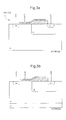
- FIGS 3a and 3b respectively show the diagrams of a transistor High-voltage n-channel MOSFET, or HVNMOS, and a p-channel MOSFET high-voltage, or HVPMOS.
- HVNMOS transistors include the advantage of a high breakdown voltage typically greater than 30 volts.
- a another advantage of this type of transistor lies in the fact that their manufacture is fully compatible with standard CMOS technology.
- the high-voltage MOSFET 202 is thus connected by its drain terminal 202b to the drain terminal 211b of the p-MOS transistor 211 of the current mirror 210 and through its source terminal 202 to the resistive element 203.
- the current generator circuit of FIG. 2 is supplied by a high supply voltage V HV - V SS of the order of ten to a few tens of Volts.
- V HV - V SS of the order of ten to a few tens of Volts.
- This supply voltage can for example be delivered by means of a high-voltage regulator circuit.
- Such a high-voltage regulator comprising an external regulation device is for example described in European patent application No. 01202429.5 filed on June 25, 2001, also in the name of the present Applicant.
- the use of the high-voltage MOSFET transistor 202 in the reference branch of the current mirror 210 makes it possible to prevent any breakdown of the components in this reference branch. Furthermore, due to the high breakdown voltage of the transistor 202 (of the order of 30 Volts), the circuit has great flexibility of use with respect to the supply voltage V HV - V SS .
- the current generator circuit 20 further comprises means, globally identified by the reference numeral 400, making it possible to limit the potential level of the output B of the circuit on which the output current I OUT is delivered to a determined extreme potential level, in particular in the case where the output is not connected to any circuit (open circuit - load resistance R L infinite).
- these means 400 are arranged to limit the potential level of the output B to a maximum value, designated V OUT, MAX , fixed by way of purely illustrative example at 10 Volts.
- the means 400 thus comprise a voltage divider circuit formed in this example of a resistive divider comprising first and second resistive elements 411 and 412, of value R 1 and R 2 , connected between the output terminal B and a third potential of reference, chosen equal to the supply potential V SS forming mass.
- the connection node between the resistive elements 411 and 412 is connected to a positive input terminal (non-inverting terminal) 401a of a second differential amplifier 401, a reference voltage V REF being applied to the negative input terminal ( inverting terminal) 401b of this differential amplifier 401.
- the reference voltage V REF (in the same way as the input voltage V IN of the current generator circuit) can for example be a voltage stable voltage reference of the type "Bandgap" well known to those skilled in the art (the so-called bandgap voltage is a voltage of the order of 1.2 Volts).
- the output terminal 401c of the differential amplifier 401 is connected to the gate 402c of a second high-voltage MOSFET transistor, also of the n-channel type, the drain of which is connected to the output B of the current generator circuit 20 and the source is connected to the supply potential V SS .
- the values R 1 and R 2 of the resistive elements 411 and 412 are chosen so as to fix the potential level of the output B at the extreme value (here maximum) V OUT, MAX designated above.
- the values R 1 and R 2 of the resistive elements 411, 412 are also chosen so as to limit the current flowing in this branch.
- the dimensioning of the components of the current generator circuit can be chosen so that the output current I QUT delivered is of the order of 10 mA.
- resistance values R1 and R2 respectively equal to 88 k ⁇ and 12 k ⁇ allow the level of maximum potential of output B at 10 Volts, while only drawing a maximum current of the order of 0.1 mA in the branch of the resistive voltage divider circuit.
- the means 400 thus ensures that the potential level of the output B of the current generator circuit does not exceed the value V OUT, MAX defined at 10 Volts in this case. Indeed, as soon as the potential level of the output exceeds the fixed threshold, the output of the differential amplifier commands the activation of the high-voltage MOSFET transistor 402 to counterbalance this increase and maintain the output B at the maximum potential level. defined.
- the current generator circuit 20 also preferably includes protection means 300 to prevent the breakdown in particular of the transistor 212 of the output branch of the current mirror 210, for example in the event of a short- ground circuit of output B of the current generator circuit.
- protection means 300 may for example comprise a cascode arrangement of one or more transistors connected in the output branch of the current mirror 210. In this example, for a supply voltage V HV - Vss of the order of 15 Volts, two additional transistors 301 and 302 connected in series with transistor 212 are sufficient.
- a resistive divider circuit 311, 312, 313 makes it possible to fix the gate potentials of the transistors 301 and 302 at suitable levels, for example 10 and 5 Volts respectively.
- the means 400 prevent the potential of the output B from rising towards V HV (in the case of an infinite load resistance R L ), which would have the consequence, for example, that the gate voltage- drain of transistor 302 may exceed a critical value.
- the means 300 and 400 thus act in a complementary manner in order to ensure the integrity of components of the current generator circuit according to this invention.
- the protection means 300 could perfectly include a third high-voltage MOSFET transistor of the transistor type 202 and 402 connected in series by its drain and source terminals in the branch of the current mirror 210.
Landscapes
- Engineering & Computer Science (AREA)
- Microelectronics & Electronic Packaging (AREA)
- Physics & Mathematics (AREA)
- Nonlinear Science (AREA)
- Electromagnetism (AREA)
- General Physics & Mathematics (AREA)
- Radar, Positioning & Navigation (AREA)
- Automation & Control Theory (AREA)
- Control Of Electrical Variables (AREA)
Abstract
Description
- la figure 1, déjà présentée, montre un diagramme schématique d'un circuit de génération de courant typique alimenté par une basse tension d'alimentation ;
- la figure 2 montre un mode de réalisation d'un circuit générateur de courant selon la présente invention ; et
- les figures 3a et 3b sont des vues en coupe schématiques de transistors MOSFET haute tension, respectivement à canal n et à canal p, réalisés selon un technologie CMOS standard.
Claims (7)
- Circuit générateur de courant (20) comprenant des moyens de génération (200, 202, 203) d'un courant de référence (IREF) et un miroir de courant (210) relié à un premier potentiel d'alimentation (VHV) et comportant une branche de référence (211) dans laquelle est appliqué ledit courant de référence (IREF) et une branche de sortie (212) délivrant, à une sortie (B) dudit circuit générateur de courant, un courant de sortie (IOUT) à l'image dudit courant de référence (IREF) et dans un rapport déterminé par rapport au dit courant de référence (IREF),
lesdits moyens de génération du courant de référence comportantcaractérisé en ce que ledit transistor MOSFET (202) est un transistor MOSFET haute-tension et en ce que le circuit générateur de courant (20) comporte en outre des moyens de limitation (400) permettant de limiter à une valeur extrême le niveau de potentiel de ladite sortie (B) du circuit générateur de courant.un transistor MOSFET (202) comprenant des terminaux de drain, de source et de grille, ce transistor MOSFET (202) étant connecté par ses terminaux de drain et de source en série dans ladite branche de référence (211) ;un élément résistif (203) connecté entre le terminal de source dudit transistor MOSFET (202) et un second potentiel d'alimentation (VSS) ; etun amplificateur différentiel (200) comportant une première entrée reliée à une tension d'entrée de référence (VIN), une seconde entrée reliée au dit terminal de source du transistor MOSFET (202), et une sortie reliée au dit terminal de grille du transistor MOSFET, - Circuit générateur de courant selon la revendication 1, caractérisé en ce que lesdits moyens de limitation (400) comportent :un circuit diviseur de tension (411, 412) connecté entre ladite sortie (B) du circuit générateur de courant et un troisième potentiel d'alimentation (VSS), et délivrant en sortie une tension divisée proportionnelle, dans un rapport déterminé, au niveau de potentiel de ladite sortie (B) du circuit générateur de courant ;un second transistor MOSFET haute-tension (402) comprenant des terminaux de drain, de source et de grille, ce second transistor MOSFET haute-tension étant connecté par ses terminaux de drain et de source entre ladite sortie (B) du circuit générateur de courant ledit troisième potentiel d'alimentation (VSS) ; etun second amplificateur différentiel (401) comportant une première entrée reliée à une tension de référence (VREF), une seconde entrée reliée à la sortie dudit circuit diviseur de tension (411, 412), et une sortie reliée au terminal de grille dudit second transistor MOSFET haute-tension (402).
- Circuit générateur de courant selon la revendication 2, caractérisé en ce que ledit circuit diviseur de tension (411, 412) est un circuit diviseur résistif.
- Circuit générateur de courant selon l'une quelconque des revendications précédentes, caractérisé en ce que le ou lesdits transistors MOSFET haute-tension sont des transistors MOSFET à canal n ou p, comprenant un oxyde de grille présentant une épaisseur plus importante du côté drain que du côté source et une zone tampon du côté drain constituée d'un caisson de type n ou p.
- Circuit générateur de courant selon l'une quelconque des revendications précédentes, caractérisé en ce que ladite branche de sortie (212) du miroir de courant (210) comporte en outre un montage cascode de un ou plusieurs transistors (301, 302).
- Circuit générateur de courant selon la revendication 2 ou 3, caractérisé en ce que ladite tension de référence (VREF) appliquée sur la première entrée du second amplificateur différentiel (401) est dérivée d'une référence de tension stable en température de type bandgap.
- Circuit générateur de courant selon l'une quelconque des revendications précédentes, caractérisé en ce que ladite tension d'entrée de référence (VIN) appliquée sur la première entrée du premier amplificateur différentiel (200) est dérivée d'une référence de tension stable en température de type bandgap.
Priority Applications (1)
| Application Number | Priority Date | Filing Date | Title |
|---|---|---|---|
| EP20010204556 EP1315062B1 (fr) | 2001-11-26 | 2001-11-26 | Circuit de génération de courant pour applications haute-tension |
Applications Claiming Priority (1)
| Application Number | Priority Date | Filing Date | Title |
|---|---|---|---|
| EP20010204556 EP1315062B1 (fr) | 2001-11-26 | 2001-11-26 | Circuit de génération de courant pour applications haute-tension |
Publications (2)
| Publication Number | Publication Date |
|---|---|
| EP1315062A1 true EP1315062A1 (fr) | 2003-05-28 |
| EP1315062B1 EP1315062B1 (fr) | 2011-05-18 |
Family
ID=8181307
Family Applications (1)
| Application Number | Title | Priority Date | Filing Date |
|---|---|---|---|
| EP20010204556 Expired - Lifetime EP1315062B1 (fr) | 2001-11-26 | 2001-11-26 | Circuit de génération de courant pour applications haute-tension |
Country Status (1)
| Country | Link |
|---|---|
| EP (1) | EP1315062B1 (fr) |
Citations (3)
| Publication number | Priority date | Publication date | Assignee | Title |
|---|---|---|---|---|
| EP0319047A2 (fr) * | 1987-12-04 | 1989-06-07 | Nissan Motor Co., Ltd. | Circuit intégré de puissance |
| US6057727A (en) * | 1997-10-20 | 2000-05-02 | Stmicroelectronics S.A. | Accurate constant current generator |
| US6087820A (en) * | 1999-03-09 | 2000-07-11 | Siemens Aktiengesellschaft | Current source |
-
2001
- 2001-11-26 EP EP20010204556 patent/EP1315062B1/fr not_active Expired - Lifetime
Patent Citations (3)
| Publication number | Priority date | Publication date | Assignee | Title |
|---|---|---|---|---|
| EP0319047A2 (fr) * | 1987-12-04 | 1989-06-07 | Nissan Motor Co., Ltd. | Circuit intégré de puissance |
| US6057727A (en) * | 1997-10-20 | 2000-05-02 | Stmicroelectronics S.A. | Accurate constant current generator |
| US6087820A (en) * | 1999-03-09 | 2000-07-11 | Siemens Aktiengesellschaft | Current source |
Also Published As
| Publication number | Publication date |
|---|---|
| EP1315062B1 (fr) | 2011-05-18 |
Similar Documents
| Publication | Publication Date | Title |
|---|---|---|
| EP0733961B1 (fr) | Générateur de courant de référence en technologie CMOS | |
| FR2755318A1 (fr) | Circuit regulateur et dispositif a circuit integre a semi-conducteur le comprenant | |
| CH697322B1 (fr) | Procédé de génération d'un courant sensiblement indépendent de la température et dispositif permettant de mettre en oeuvre ce procédé. | |
| EP0424264B1 (fr) | Source de courant à faible coefficient de température | |
| FR2890259A1 (fr) | Circuit de generation d'un courant de reference et circuit de polarisation | |
| EP0788047B1 (fr) | Dispositif de référence de courant en circuit intégré | |
| FR2862448A1 (fr) | Generateur de rampe de tension avec un asservissement de pente | |
| EP0583203B1 (fr) | Circuit de tirage vers un état déterminé d'une entrée de circuit intégré | |
| EP0700151A1 (fr) | Etage amplificateur de puissance, de type suiveur | |
| EP0678802A1 (fr) | Circuit de limitation de tension avec comparateur à hystérésis | |
| FR2678399A1 (fr) | Miroir de courant fonctionnant sous faible tension. | |
| EP0756223A1 (fr) | Générateur de référence de tension et/ou de courant en circuit intégré | |
| EP2913849B1 (fr) | Dispositif electronique avec transistor hemt polarisé en inverse | |
| FR2825806A1 (fr) | Circuit de polarisation a point de fonctionnement stable en tension et en temperature | |
| EP0687967B1 (fr) | Source de courant stable en température | |
| FR2797086A1 (fr) | Cellule logique a programmation unique | |
| EP0571302A1 (fr) | Amplificateur avec limitation de courant de sortie | |
| EP1315062B1 (fr) | Circuit de génération de courant pour applications haute-tension | |
| FR2795557A1 (fr) | Dispositif d'ajustement des circuits apres mise en boitier et procede de fabrication correspondant | |
| EP0738038A1 (fr) | Amplificateur de courant | |
| FR2744299A1 (fr) | Convertisseur continu/continu a faible tension d'alimentation | |
| FR2648643A1 (fr) | Circuit d'interface entre deux circuits numeriques de natures differentes | |
| FR2802315A1 (fr) | Regulateur de tension a transistor ballast et a limiteur de courant | |
| FR2757964A1 (fr) | Regulateur de tension serie | |
| FR2872648A1 (fr) | Amplificateur a transconductance rapide |
Legal Events
| Date | Code | Title | Description |
|---|---|---|---|
| PUAI | Public reference made under article 153(3) epc to a published international application that has entered the european phase |
Free format text: ORIGINAL CODE: 0009012 |
|
| AK | Designated contracting states |
Designated state(s): AT BE CH CY DE DK ES FI FR GB GR IE IT LI LU MC NL PT SE TR |
|
| AX | Request for extension of the european patent |
Extension state: AL LT LV MK RO SI |
|
| 17P | Request for examination filed |
Effective date: 20031128 |
|
| AKX | Designation fees paid |
Designated state(s): CH DE FR GB IT LI |
|
| 17Q | First examination report despatched |
Effective date: 20060707 |
|
| GRAP | Despatch of communication of intention to grant a patent |
Free format text: ORIGINAL CODE: EPIDOSNIGR1 |
|
| GRAS | Grant fee paid |
Free format text: ORIGINAL CODE: EPIDOSNIGR3 |
|
| GRAA | (expected) grant |
Free format text: ORIGINAL CODE: 0009210 |
|
| AK | Designated contracting states |
Kind code of ref document: B1 Designated state(s): CH DE FR GB IT LI |
|
| REG | Reference to a national code |
Ref country code: GB Ref legal event code: FG4D Free format text: NOT ENGLISH |
|
| REG | Reference to a national code |
Ref country code: CH Ref legal event code: EP Ref country code: CH Ref legal event code: NV Representative=s name: ICB INGENIEURS CONSEILS EN BREVETS SA |
|
| REG | Reference to a national code |
Ref country code: DE Ref legal event code: R096 Ref document number: 60144656 Country of ref document: DE Effective date: 20110630 |
|
| PLBE | No opposition filed within time limit |
Free format text: ORIGINAL CODE: 0009261 |
|
| STAA | Information on the status of an ep patent application or granted ep patent |
Free format text: STATUS: NO OPPOSITION FILED WITHIN TIME LIMIT |
|
| 26N | No opposition filed |
Effective date: 20120221 |
|
| PG25 | Lapsed in a contracting state [announced via postgrant information from national office to epo] |
Ref country code: IT Free format text: LAPSE BECAUSE OF FAILURE TO SUBMIT A TRANSLATION OF THE DESCRIPTION OR TO PAY THE FEE WITHIN THE PRESCRIBED TIME-LIMIT Effective date: 20110518 |
|
| REG | Reference to a national code |
Ref country code: DE Ref legal event code: R097 Ref document number: 60144656 Country of ref document: DE Effective date: 20120221 |
|
| GBPC | Gb: european patent ceased through non-payment of renewal fee |
Effective date: 20121126 |
|
| PG25 | Lapsed in a contracting state [announced via postgrant information from national office to epo] |
Ref country code: GB Free format text: LAPSE BECAUSE OF NON-PAYMENT OF DUE FEES Effective date: 20121126 |
|
| REG | Reference to a national code |
Ref country code: FR Ref legal event code: PLFP Year of fee payment: 15 |
|
| REG | Reference to a national code |
Ref country code: FR Ref legal event code: PLFP Year of fee payment: 16 |
|
| REG | Reference to a national code |
Ref country code: FR Ref legal event code: PLFP Year of fee payment: 17 |
|
| REG | Reference to a national code |
Ref country code: FR Ref legal event code: PLFP Year of fee payment: 18 |
|
| PGFP | Annual fee paid to national office [announced via postgrant information from national office to epo] |
Ref country code: DE Payment date: 20191021 Year of fee payment: 19 |
|
| PGFP | Annual fee paid to national office [announced via postgrant information from national office to epo] |
Ref country code: FR Payment date: 20191022 Year of fee payment: 19 |
|
| PGFP | Annual fee paid to national office [announced via postgrant information from national office to epo] |
Ref country code: CH Payment date: 20191022 Year of fee payment: 19 |
|
| REG | Reference to a national code |
Ref country code: DE Ref legal event code: R119 Ref document number: 60144656 Country of ref document: DE |
|
| REG | Reference to a national code |
Ref country code: CH Ref legal event code: PL |
|
| PG25 | Lapsed in a contracting state [announced via postgrant information from national office to epo] |
Ref country code: LI Free format text: LAPSE BECAUSE OF NON-PAYMENT OF DUE FEES Effective date: 20201130 Ref country code: CH Free format text: LAPSE BECAUSE OF NON-PAYMENT OF DUE FEES Effective date: 20201130 |
|
| PG25 | Lapsed in a contracting state [announced via postgrant information from national office to epo] |
Ref country code: FR Free format text: LAPSE BECAUSE OF NON-PAYMENT OF DUE FEES Effective date: 20201130 |
|
| PG25 | Lapsed in a contracting state [announced via postgrant information from national office to epo] |
Ref country code: DE Free format text: LAPSE BECAUSE OF NON-PAYMENT OF DUE FEES Effective date: 20210601 |