EP1314342B1 - Method, apparatus and use of applying viscous medium on a substrate - Google Patents
Method, apparatus and use of applying viscous medium on a substrate Download PDFInfo
- Publication number
- EP1314342B1 EP1314342B1 EP01950142A EP01950142A EP1314342B1 EP 1314342 B1 EP1314342 B1 EP 1314342B1 EP 01950142 A EP01950142 A EP 01950142A EP 01950142 A EP01950142 A EP 01950142A EP 1314342 B1 EP1314342 B1 EP 1314342B1
- Authority
- EP
- European Patent Office
- Prior art keywords
- jetting
- viscous medium
- substrate
- screen printing
- correction
- Prior art date
- Legal status (The legal status is an assumption and is not a legal conclusion. Google has not performed a legal analysis and makes no representation as to the accuracy of the status listed.)
- Expired - Lifetime
Links
Images
Classifications
-
- B—PERFORMING OPERATIONS; TRANSPORTING
- B23—MACHINE TOOLS; METAL-WORKING NOT OTHERWISE PROVIDED FOR
- B23K—SOLDERING OR UNSOLDERING; WELDING; CLADDING OR PLATING BY SOLDERING OR WELDING; CUTTING BY APPLYING HEAT LOCALLY, e.g. FLAME CUTTING; WORKING BY LASER BEAM
- B23K3/00—Tools, devices, or special appurtenances for soldering, e.g. brazing, or unsoldering, not specially adapted for particular methods
- B23K3/06—Solder feeding devices; Solder melting pans
- B23K3/0607—Solder feeding devices
-
- H—ELECTRICITY
- H05—ELECTRIC TECHNIQUES NOT OTHERWISE PROVIDED FOR
- H05K—PRINTED CIRCUITS; CASINGS OR CONSTRUCTIONAL DETAILS OF ELECTRIC APPARATUS; MANUFACTURE OF ASSEMBLAGES OF ELECTRICAL COMPONENTS
- H05K3/00—Apparatus or processes for manufacturing printed circuits
- H05K3/30—Assembling printed circuits with electric components, e.g. with resistor
- H05K3/32—Assembling printed circuits with electric components, e.g. with resistor electrically connecting electric components or wires to printed circuits
- H05K3/34—Assembling printed circuits with electric components, e.g. with resistor electrically connecting electric components or wires to printed circuits by soldering
- H05K3/3457—Solder materials or compositions; Methods of application thereof
- H05K3/3485—Applying solder paste, slurry or powder
-
- B—PERFORMING OPERATIONS; TRANSPORTING
- B23—MACHINE TOOLS; METAL-WORKING NOT OTHERWISE PROVIDED FOR
- B23K—SOLDERING OR UNSOLDERING; WELDING; CLADDING OR PLATING BY SOLDERING OR WELDING; CUTTING BY APPLYING HEAT LOCALLY, e.g. FLAME CUTTING; WORKING BY LASER BEAM
- B23K2101/00—Articles made by soldering, welding or cutting
- B23K2101/36—Electric or electronic devices
- B23K2101/40—Semiconductor devices
-
- H—ELECTRICITY
- H05—ELECTRIC TECHNIQUES NOT OTHERWISE PROVIDED FOR
- H05K—PRINTED CIRCUITS; CASINGS OR CONSTRUCTIONAL DETAILS OF ELECTRIC APPARATUS; MANUFACTURE OF ASSEMBLAGES OF ELECTRICAL COMPONENTS
- H05K1/00—Printed circuits
- H05K1/02—Details
- H05K1/0266—Marks, test patterns or identification means
- H05K1/0269—Marks, test patterns or identification means for visual or optical inspection
-
- H—ELECTRICITY
- H05—ELECTRIC TECHNIQUES NOT OTHERWISE PROVIDED FOR
- H05K—PRINTED CIRCUITS; CASINGS OR CONSTRUCTIONAL DETAILS OF ELECTRIC APPARATUS; MANUFACTURE OF ASSEMBLAGES OF ELECTRICAL COMPONENTS
- H05K2203/00—Indexing scheme relating to apparatus or processes for manufacturing printed circuits covered by H05K3/00
- H05K2203/01—Tools for processing; Objects used during processing
- H05K2203/0104—Tools for processing; Objects used during processing for patterning or coating
- H05K2203/0126—Dispenser, e.g. for solder paste, for supplying conductive paste for screen printing or for filling holes
-
- H—ELECTRICITY
- H05—ELECTRIC TECHNIQUES NOT OTHERWISE PROVIDED FOR
- H05K—PRINTED CIRCUITS; CASINGS OR CONSTRUCTIONAL DETAILS OF ELECTRIC APPARATUS; MANUFACTURE OF ASSEMBLAGES OF ELECTRICAL COMPONENTS
- H05K2203/00—Indexing scheme relating to apparatus or processes for manufacturing printed circuits covered by H05K3/00
- H05K2203/14—Related to the order of processing steps
- H05K2203/1476—Same or similar kind of process performed in phases, e.g. coarse patterning followed by fine patterning
-
- H—ELECTRICITY
- H05—ELECTRIC TECHNIQUES NOT OTHERWISE PROVIDED FOR
- H05K—PRINTED CIRCUITS; CASINGS OR CONSTRUCTIONAL DETAILS OF ELECTRIC APPARATUS; MANUFACTURE OF ASSEMBLAGES OF ELECTRICAL COMPONENTS
- H05K2203/00—Indexing scheme relating to apparatus or processes for manufacturing printed circuits covered by H05K3/00
- H05K2203/16—Inspection; Monitoring; Aligning
- H05K2203/163—Monitoring a manufacturing process
-
- H—ELECTRICITY
- H05—ELECTRIC TECHNIQUES NOT OTHERWISE PROVIDED FOR
- H05K—PRINTED CIRCUITS; CASINGS OR CONSTRUCTIONAL DETAILS OF ELECTRIC APPARATUS; MANUFACTURE OF ASSEMBLAGES OF ELECTRICAL COMPONENTS
- H05K3/00—Apparatus or processes for manufacturing printed circuits
- H05K3/10—Apparatus or processes for manufacturing printed circuits in which conductive material is applied to the insulating support in such a manner as to form the desired conductive pattern
- H05K3/12—Apparatus or processes for manufacturing printed circuits in which conductive material is applied to the insulating support in such a manner as to form the desired conductive pattern using thick film techniques, e.g. printing techniques to apply the conductive material or similar techniques for applying conductive paste or ink patterns
- H05K3/1216—Apparatus or processes for manufacturing printed circuits in which conductive material is applied to the insulating support in such a manner as to form the desired conductive pattern using thick film techniques, e.g. printing techniques to apply the conductive material or similar techniques for applying conductive paste or ink patterns by screen printing or stencil printing
-
- Y—GENERAL TAGGING OF NEW TECHNOLOGICAL DEVELOPMENTS; GENERAL TAGGING OF CROSS-SECTIONAL TECHNOLOGIES SPANNING OVER SEVERAL SECTIONS OF THE IPC; TECHNICAL SUBJECTS COVERED BY FORMER USPC CROSS-REFERENCE ART COLLECTIONS [XRACs] AND DIGESTS
- Y10—TECHNICAL SUBJECTS COVERED BY FORMER USPC
- Y10T—TECHNICAL SUBJECTS COVERED BY FORMER US CLASSIFICATION
- Y10T29/00—Metal working
- Y10T29/49—Method of mechanical manufacture
- Y10T29/49002—Electrical device making
- Y10T29/49117—Conductor or circuit manufacturing
- Y10T29/49124—On flat or curved insulated base, e.g., printed circuit, etc.
- Y10T29/4913—Assembling to base an electrical component, e.g., capacitor, etc.
- Y10T29/49144—Assembling to base an electrical component, e.g., capacitor, etc. by metal fusion
Landscapes
- Engineering & Computer Science (AREA)
- Mechanical Engineering (AREA)
- Manufacturing & Machinery (AREA)
- Microelectronics & Electronic Packaging (AREA)
- Application Of Or Painting With Fluid Materials (AREA)
- Screen Printers (AREA)
- Electric Connection Of Electric Components To Printed Circuits (AREA)
- Manufacturing Of Printed Wiring (AREA)
- Printing Methods (AREA)
- Ink Jet (AREA)
- Non-Metallic Protective Coatings For Printed Circuits (AREA)
- Coating Apparatus (AREA)
Abstract
Description
- The present invention generally relates to the field of providing substrates with viscous medium. More specifically, the invention relates to a method of applying a viscous medium on a substrate, said method comprising the step of screen printing predetermined amounts of the viscous medium on predetermined positions on the substrate; an apparatus for application of a viscous medium onto a substrate, said apparatus comprising screen printing means for screen printing predetermined amounts of the viscous medium on predetermined positions on the substrate; and an apparatus for application of additional viscous medium onto a screen printed substrate.
- The most common method of applying viscous medium, such as solder paste, to a substrate, such as a PCB, in electronics production is by using screen printing. The vast majority of viscous medium deposits can be applied by this method. However, in specific circumstances there is a need for different viscous mediums at different locations on the substrate. This poses a problem, since there are a number of difficulties to overcome when adding viscous medium by performing an extra screen printing procedure, after an initial application of viscous medium. Further, it is sometimes desired to produce patterns of viscous medium that are very difficult to achieve through screen printing, such as the pattern of an unfilled circle.
- It can also be desired that the applied viscous medium presents different heights at different positions on the substrate in order to accommodate, e.g., chip components having different heights, components having different lead angle accuracy, or co-planarity requirements. A solution to the latter problem that has been suggested in the art is to use so called stepped stencils for the screen printing. However, these stencils present a number of drawbacks that have prevented widespread use of this solution.
- Also, the application of very small deposits, primarily circular, i.e. dots, of viscous medium is not possible to obtain through screen printing, since the adhesion forces from the stencil would become to great in comparison to the adhesion forces from the substrate. As a consequence, very small deposits would attach to and follow the stencil when the stencil is removed. It could be imagined that this problem is overcome by using a thinner stencil. However, that would have undesired drawbacks in that it would result in an overall decrease of the height of the deposits, and thus the overall volume, which is undesired and would pose a problem for larger deposits.
- According to the state of the art, efforts have been made to solve the above stated problems by using a conventional dispensing equipment. By using a conventional dispenser it is possible to add viscous medium following an initial screen printing of the substrate for producing said patterns of viscous medium that are not easily achieved through screen printing. With a conventional dispenser it can also be possible to apply viscous medium having different height at different locations on the board. However, the conventional dispensers have a number of disadvantages. The process of conventional dispensing of viscous medium is relatively slow, the application of very small deposits of viscous medium through conventional dispensing is difficult, and it is also difficult to apply additional viscous medium onto a location on the substrate that has already been provided with viscous medium.
- Thus, an object of the present invention is to provide a solution to the above stated problems in relation to the application of additional viscous medium to a substrate that already has been subject to initial application of viscous medium through screen printing.
- This and other objects are achieved according to the present invention by providing a method and an apparatus having the features defined in the independent claims. Preferred embodiments are defined in the dependent claims.
- According to the invention, there is provided a method of applying viscous medium on a substrate, comprising the steps of screen printing predetermined amounts of the viscous medium on predetermined positions on the substrate, and add-on jetting of predetermined additional amounts of viscous medium on predetermined positions on the screen printed substrate.
- According to the invention, there is further provided an apparatus for application of a viscous medium onto a substrate, comprising screen printing means for screen printing predetermined amounts of the viscous medium on predetermined positions on the substrate, and jetting means for jetting predetermined additional amounts of viscous medium on predetermined positions on the screen printed substrate.
- According to the invention, there is also provided an apparatus for application of additional viscous medium onto a screen printed substrate, comprising jetting means for jetting said additional amounts of viscous medium on predetermined positions on the screen printed substrate.
- According to the invention, there is further provided use of screen printing and subsequent jetting for applying a viscous medium on a substrate.
- According to the invention, there is still provided use of viscous medium jetting for applying additional viscous medium on a screen printed substrate.
- For the purposes of this application, it is to be noted that the term "viscous medium" should be interpreted as solder paste, flux, adhesive, conductive adhesive, or any other kind of medium used for fastening components on a substrate, or resistive paste; and that the term "substrate" should be interpreted as a printed circuit board (PCB), a substrate for ball grid arrays (BGA), chip scale packages (CSP), quad flat packages (QFP), and flip-chips or the like. It is also to be noted that the term "jetting" should be interpreted as a non-contact dispensing process that utilises a fluid jet to form and shoot droplets of a viscous medium from a jet nozzle onto a substrate, e.g. as described in the published International Application
WO 99/64167 - Thus, the present invention is based on the advantageous idea of using add-on jetting for the application of additional viscous medium onto a substrate onto which viscous medium previously has been applied through screen printing.
- The use of jetting overcomes a number of the above stated problems relating to screen printing. First, jetting enables the application of viscous medium of a different type or sort than what has been initially applied. The use of jetting also enables the application of viscous medium in any desired pattern, which is not possible through screen printing. The application of viscous medium of varying height is also achievable through jetting. Also, jetting is advantageous to conventional dispensing in that it is faster, more accurate, and more flexible. In fact, the use of conventional dispensing often provide a bottle neck that increases the cycle time in the overall component mounting process, as compared to the use of jetting. It has also been found that it is possible to achieve smaller dots when using jetting than when using conventional dispensing.
- Further, one of the main advantages obtained by using jetting for applying additional viscous medium onto a screen printed substrate, is that it is possible to apply viscous medium at positions where viscous medium already has been applied. Thereby, it will be possible to easily increase the height of the applied viscous medium at a specific location without any danger of the nozzle of the jetting device being smeared by the viscous medium already applied on the substrate.
- According to a specific embodiment of the present invention, the results of the application of viscous medium onto the substrate is inspected, errors of the application is determined based on said inspection, and at least some of said errors are corrected, wherein said correction comprises jetting of additional viscous medium onto the substrate. This means that not only the predetermined additional amounts of viscous medium is applied onto the substrate through jetting, but also any additional amount of viscous medium that is determined to be required as a result of errors in the regular viscous medium application.
- Said inspection can be performed between the screen printing and the add-on jetting of viscous medium, following the add-on jetting of viscous medium, or both. If the inspection is performed between the screen printing and the add-on jetting, the predetermined add-on jetting can be combined with the correction jetting, either by determining the positions where jetting is required and the amount, or by performing the add-on jetting and the jetting correction in sequence.
- Preferably, a single jetting means performs both the add-on jetting and the jetting correction, which decreases the physical complexity of the system. Alternatively, this is performed by separate jetting means.
- When the inspection is performed following the add-on jetting only, the correction can be performed in a separate machine. This decreases the cycle time for the overall viscous medium application process, but increases the line length. If a separate machine is used for the jetting correction, the inspection, evaluation and determination of errors is preferably, but not necessarily, performed in the same machine.
- According to a further embodiment of the invention, the correction of applied viscous medium also comprises the removal of surplus viscous medium. Preferably, this is performed at specific locations on the substrate only, at which the inspection has revealed that too much viscous medium has been applied. This can refer to the amount of viscous medium for a given location, the height of the applied viscous medium, the applied viscous medium being offset from the intended position, or that viscous medium has been applied at a position where it was not supposed to.
- According to a further embodiment of the present invention, following the inspection of a substrate, an evaluation is performed to determine whether the number or the severity of detected errors are such that correction of applied viscous medium is worthwhile. Such an evaluation can be performed regardless of whether the inspection is performed before or after the add-on jetting of additional viscous medium. That is, if there are a large number of corrective actions required, then it might be more economical to simply discard the substrate. This is of course dependent on the type of substrate and the cost involved for the substrate. If correction is not deemed worthwhile, the substrate is preferably cleaned from any applied viscous medium and reused. On the other hand, if cleaning the substrate is not considered economical, the substrate is preferably discarded.
- It should be noted that the screen printing and the subsequent jetting of viscous medium is for the purposes of this application not limited to the use of one viscous medium for both the screen printing and the jetting. Consequently, a number of different types and sorts of viscous medium can be used. For instance, the screen printing is performed for a viscous medium, then add-on jetting of another viscous medium is performed. Additionally, the subsequent jetting, the add-on jetting and/or the correction jetting, can be performed in sequences with different sorts of viscous medium. Then, more than one jetting means is preferably used to avoid unwanted mixing of the different viscous medium and/or to avoid increased cycle time due to change of the viscous medium supply and possible cleaning of the jetting means.
- The above mentioned and other aspects, advantages, and features of the invention will be more fully understood from the following description of exemplifying embodiments thereof.
- Exemplifying embodiments of the invention will be described below with reference to the accompanying drawings, in which:
-
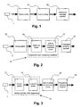
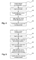
Figs 1-3 are block diagrams illustrating arrangements according to alternative embodiments of the present invention. -
Figs 4-6 illustrate in flow chart form the alternative embodiments shown inFigs 1-3 . - In the block diagrams of
Figs 1-3 , the thick-lined arrows depict the movement of asubstrate 1 through the production line. The dashed boxes simply indicate that the means or apparatus depicted within the box can be incorporated in a single machine. - With reference to
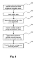
Figs 1-6 , there are illustrated exemplary embodiments of the present invention. As to the specific means used for screen printing, jetting, inspection of application results, removing solder paste, and component mounting, use can be made of suitable means which by themselves are known within the art, and the constructional features of which are also known. Therefore, detailed constructional and functional description of each separate means have been omitted. Furthermore, the viscous medium of the description of exemplary embodiments below is solder paste. However, the invention is not restricted to using solder paste. On the contrary, any type of viscous medium can be used. - Turning first to
Figs 1 and4 , there is shown a first exemplary embodiment of the present invention. Asubstrate 1 is atstep 100 transferred to ascreen printer 12 where an initial application of solder paste is performed, atstep 102. Then, thesubstrate 1 is transferred atstep 104 to amachine 16 for performing add-on jetting of additional amounts of solder paste, atstep 106. The amounts, patterns, heights, type of solder paste, etc., that is added onto thesubstrate 1 is predetermined. Thus, there is no inspection if the screen printing results performed prior to the jetting of additional solder paste. Following the add-on jetting step, thesubstrate 1 is atstep 108 transferred to acomponent mounting machine 18, where electrical components are mounted on thesubstrate 1. As an alternative, there may be included a step of inspecting the final results of the combined solder paste application, i.e. both the screen printing and the add-on jetting. - With reference now to
Figs 2 and5 , there is shown another exemplary embodiment of the present invention. This embodiment also includes inspection means 14 provided for inspection of the screen printing results. Following screen printing atstep 202, the substrate is atstep 204 transferred to inspection means 14 that performs the inspection atstep 206. The results of the inspection is recorded and relayed to the means 16' for performing the add-on jetting. With the information as to the results of said inspection, the jetting means 16' can also perform any required jetting of additional solder paste onto positions on the substrate where insufficient amounts have been applied due to some error in the initial screen printing. Thus, the jetting means 16' is a combined add-on jetting and correction means 16'. Further, according to this embodiment, the add-on jetting and correction means 16' can also comprise means for removing amounts of solder paste from the substrate. According to this embodiment, the removal is performed through suction of the solder paste at the selected position of the substrate. If the inspection reveals that correction of thesubstrate 1 is not worthwhile, thesubstrate 1 is passed by the add-on jetting and correction means 16' without any measures taking place. Then, thesubstrate 1 is simply taken out of the production line before reaching thecomponent mounting machine 18. - The inspection means 14 is preferably incorporated in the same machine as the add-on jetting and correction means 16', thus forming a combined inspection and
correction machine 15. Then, the inspection means 14 could be used to inspect the result of the add-on jetting to further minimise the application errors on the substrate. However, the inspection means 14 can naturally also be a separate machine. - Following the correction and add-on jetting, at
step 208, the substrate is transferred to thecomponent mounting machine 18, atstep 210. - Finally, the block diagram of
Fig. 3 and the flow chart ofFig. 6 illustrate yet another exemplary embodiment of the present invention. Here, thescreen printer 12 and the inspection means 14 is incorporated in asingle machine 10. Following the screen printing of thesubstrate 1 and the subsequent inspection of the screen printing results in the screen printer and inspection means 10, at steps 300-304, thesubstrate 1 is transferred to an add-on jetting and correction means 16'. The add-on jetting and correction means 16' have the similar features as do the corresponding means 16' ofFig. 2 . When the substrate enters the add-on jetting and correction means 16', said means 16' has received information as to the required corrections, if any, to be performed on thesubstrate 1. The additional solder paste is then added and any application errors corrected, atstep 308, and thesubstrate 1 is transferred atstep 310 to thecomponent mounting machine 18. Again, if the inspection reveals that thesubstrate 1 is provided with a number of errors resulting from the screen printing, and that correction is deemed not to be worthwhile, thesubstrate 1 is taken out of the production line. In this embodiment, this is performed before thesubstrate 1 reaches the add-on jetting and correction means 16'. - As is understood by the man skilled in the art, the above-mentioned steps would require a certain amount of processing, transferring and evaluating information. This, however, can be performed by conventional processing means which is not shown or further described.
Claims (20)
- A method of applying viscous medium on a substrate, e.g., a PCB comprising the steps of
screen printing predetermined amounts of a viscous medium on predetermined positions on the substrate, and
add-on jetting of predetermined additional amounts of viscous medium on predetermined positions on the screen printed substrate. - The method according to claim 1, comprising the steps of
inspecting the results of said screen printing and add-on jetting,
determining errors of said screen printing and add-on jetting based on said inspection,
determining whether correction is required, and
correcting, if correction is required, at least some of said errors, wherein said correction comprises supplemental jetting of additional viscous medium onto the screen printed substrate. - The method according to claim 1, comprising the steps of
inspecting the results of said screen printing prior to said add-on jetting,
determining errors of said screen printing based on said inspection,
and determining whether correction is required, and
correcting, if correction is required, at least some of said errors, wherein said correcting comprises supplemental jetting of additional viscous medium onto the screen printed substrate. - The method according to claim 3, wherein said supplemental jetting is performed in connection with performing said add-on jetting.
- The method according to any one of claims 2-4, wherein said add-on jetting and said supplemental jetting is performed by the same jetting means.
- The method according to any one of claims 2-5, wherein said step of correcting comprises the step of,
removing amounts of viscous medium from positions on the substrate. - The method according to any one of claims 2-6, wherein said step of determining whether correction is required comprises the step of
evaluating all of the determined errors and deciding on whether the determined errors shall be corrected. - The method according to any one of the preceding claims, wherein at least one viscous medium applied through said add-on jetting is different from the viscous medium applied through screen printing.
- An apparatus for application of viscous medium onto a substrate, e.g., a PCB
comprising screen printing means for screen printing predetermined amounts of a viscous medium on predetermined positions on the substrate, and
jetting means for jetting predetermined additional amounts of viscous medium on predetermined positions on the screen printed substrate. - The apparatus according to claim 9, comprising
inspection means for inspecting the results of said screen printing and jetting,
processing means for determining errors of said screen printing and jetting based on said inspection, and
correction means for correcting at least some of said errors, wherein said correction means comprises jetting means arranged for supplemental jetting of amounts of viscous medium onto the screen printed substrate. - The apparatus according to claim 9, comprising
inspection means for inspecting the results of said screen printing,
processing means for determining errors of said screen printing based on said inspection, and
correction means for correcting at least some of said errors, wherein said correction means comprises jetting means arranged for supplemental jetting of amounts of viscous medium onto the screen printed substrate. - The apparatus according to claim 10 or 11, wherein the correction means comprises removing means for removing viscous medium from the screen printed substrate.
- The apparatus according to any one of claims 10-12, wherein the jetting means for jetting additional amounts of viscous medium on predetermined positions on the substrate and the supplemental jetting means is the same jetting means.
- An apparatus for application of additional viscous medium onto a screen printed substrate, comprising jetting means for jetting said additional amounts of viscous medium on predetermined positions on the substrate.
- The apparatus according to claim 14, comprising
inspection means for inspecting the results of said screen printing and jetting,
processing means for determining errors of said screen printing and jetting based on said inspection, and
correction means for correcting at least some of said errors, wherein said correction means comprises jetting means arranged for supplemental jetting of amounts of viscous medium onto the screen printed substrate. - The apparatus according to claim 14, comprising
inspection means for inspecting the results of said screen printing,
processing means for determining errors of said screen printing based on said inspection, and
correction means for correcting at least some of said errors, wherein said correction means comprises jetting means arranged for supplemental jetting of amounts of viscous medium onto the screen printed substrate. - The apparatus according to claim 15 or 16, wherein the correction means comprises removing means for removing viscous medium from the screen printed substrate.
- The apparatus according to any one of claims 15-17, wherein the jetting means for jetting additional amounts of viscous medium on predetermined positions on the substrate and the supplemental jetting means is the same jetting means.
- Use of screen printing and subsequent jetting for applying a viscous medium on a substrate e.g., a PCB
- Use of viscous medium jetting for applying additional viscous medium on a screen printed substrate e.g., a PCB
Applications Claiming Priority (3)
| Application Number | Priority Date | Filing Date | Title |
|---|---|---|---|
| SE0002619A SE518640C2 (en) | 2000-07-11 | 2000-07-11 | Method, apparatus for applying a viscous medium to a substrate, apparatus for applying additional viscous medium and the use of screen printing |
| SE0002619 | 2000-07-11 | ||
| PCT/SE2001/001567 WO2002005608A1 (en) | 2000-07-11 | 2001-07-06 | Method, apparatus and use of applying viscous medium on a substrate |
Publications (2)
| Publication Number | Publication Date |
|---|---|
| EP1314342A1 EP1314342A1 (en) | 2003-05-28 |
| EP1314342B1 true EP1314342B1 (en) | 2008-08-20 |
Family
ID=20280455
Family Applications (1)
| Application Number | Title | Priority Date | Filing Date |
|---|---|---|---|
| EP01950142A Expired - Lifetime EP1314342B1 (en) | 2000-07-11 | 2001-07-06 | Method, apparatus and use of applying viscous medium on a substrate |
Country Status (8)
| Country | Link |
|---|---|
| US (2) | US7757391B2 (en) |
| EP (1) | EP1314342B1 (en) |
| JP (1) | JP5198709B2 (en) |
| AT (1) | ATE406085T1 (en) |
| AU (1) | AU2001271170A1 (en) |
| DE (1) | DE60135467D1 (en) |
| SE (1) | SE518640C2 (en) |
| WO (1) | WO2002005608A1 (en) |
Cited By (1)
| Publication number | Priority date | Publication date | Assignee | Title |
|---|---|---|---|---|
| WO2011054432A1 (en) * | 2009-11-06 | 2011-05-12 | Ekra Automatisierungssysteme Gmbh | Method and apparatus for printing a substrate, in particular a printed circuit board, with a printing paste |
Families Citing this family (15)
| Publication number | Priority date | Publication date | Assignee | Title |
|---|---|---|---|---|
| SE518642C2 (en) | 2000-07-11 | 2002-11-05 | Mydata Automation Ab | Method, device for providing a substrate with viscous medium, device for correcting application errors and the use of projecting means for correcting application errors |
| JP4618085B2 (en) * | 2005-09-30 | 2011-01-26 | 株式会社日立プラントテクノロジー | Solder paste printing system |
| US8453595B2 (en) * | 2005-11-14 | 2013-06-04 | Mydata Automation Ab | Jetting apparatus and method of improving the performance of a jetting apparatus |
| JP4869776B2 (en) * | 2006-04-28 | 2012-02-08 | ヤマハ発動機株式会社 | Printing inspection apparatus and printing apparatus |
| US7823762B2 (en) * | 2006-09-28 | 2010-11-02 | Ibiden Co., Ltd. | Manufacturing method and manufacturing apparatus of printed wiring board |
| KR100807090B1 (en) * | 2007-03-28 | 2008-02-26 | 에스엔유 프리시젼 주식회사 | A device for supporting substrate and examiner for seal pattern of lcd cell using the same |
| US9398697B2 (en) | 2013-03-13 | 2016-07-19 | Mycronic AB | Methods and devices for jetting viscous medium on workpiece |
| EP3032933B8 (en) * | 2013-08-07 | 2018-11-14 | FUJI Corporation | Electronic component mounting machine and transfer confirmation method |
| JP6155468B2 (en) * | 2013-12-06 | 2017-07-05 | パナソニックIpマネジメント株式会社 | Electronic component mounting method and electronic component mounting system |
| JP2015109397A (en) * | 2013-12-06 | 2015-06-11 | パナソニックIpマネジメント株式会社 | Electronic component mounting method and electronic component mounting system |
| DE102014202170A1 (en) * | 2014-02-06 | 2015-08-20 | Ekra Automatisierungssysteme Gmbh | Apparatus and method for printing on substrates |
| JP2017535066A (en) * | 2014-09-09 | 2017-11-24 | マイクロニック アーベーMycronic Ab | Method and apparatus for applying solder paste flux |
| CN112040760B (en) * | 2014-11-20 | 2022-04-01 | 株式会社高迎科技 | Inspection device and component mounting system with same |
| DE102016116201B4 (en) * | 2016-08-31 | 2018-06-21 | Asm Assembly Systems Gmbh & Co. Kg | A method of applying paste material to a substrate and supplementing application of paste material to a paste deposit of the substrate, controller, computer program product and screen printer |
| US11544836B2 (en) * | 2021-03-18 | 2023-01-03 | Inventec (Pudong) Technology Corporation | Grid clustering-based system for locating an abnormal area of solder paste printing and method thereof |
Family Cites Families (51)
| Publication number | Priority date | Publication date | Assignee | Title |
|---|---|---|---|---|
| US3580462A (en) | 1967-12-14 | 1971-05-25 | Louis Vanyi | Soldering apparatus |
| GB1270926A (en) * | 1968-04-05 | 1972-04-19 | Johnson Matthey Co Ltd | Improvements in and relating to a method of making metal articles |
| US3738760A (en) * | 1971-10-13 | 1973-06-12 | Plastic Kote Co | Paint touch-up container |
| US3962487A (en) * | 1975-02-03 | 1976-06-08 | Texas Instruments Incorporated | Method of making ceramic semiconductor elements with ohmic contact surfaces |
| US4239827A (en) * | 1979-01-15 | 1980-12-16 | Union Carbide Corporation | Flame-sprayed thermoplastic substrate is coated with an adhesive layer which bonds particles of an adsorbent like carbon to the substrate |
| FR2552345B1 (en) * | 1983-09-27 | 1985-12-20 | Sames Sa | ELECTROSTATIC PAINT APPARATUS WITH PNEUMATIC SPRAYER ON MOBILE SUPPORT, ADJUSTABLE IN OPERATION |
| JPH07109935B2 (en) | 1989-01-27 | 1995-11-22 | オムロン株式会社 | Method and apparatus for automatically correcting solder defects |
| SE465713B (en) * | 1990-02-12 | 1991-10-21 | Mydata Automation Ab | DEVICE FOR PREPARING PASTORS AND LIMS |
| JPH03297102A (en) * | 1990-04-17 | 1991-12-27 | Cmk Corp | Formation of carbon resistor in printed wiring board |
| JPH04239797A (en) | 1991-01-23 | 1992-08-27 | Sharp Corp | Screen printing device |
| US5097516A (en) * | 1991-02-28 | 1992-03-17 | At&T Bell Laboratories | Technique for illuminating a surface with a gradient intensity line of light to achieve enhanced two-dimensional imaging |
| US5155904A (en) * | 1991-04-03 | 1992-10-20 | Compaq Computer Corporation | Reflow and wave soldering techniques for bottom side components |
| US5108024A (en) | 1991-06-03 | 1992-04-28 | Motorola, Inc. | Method of inspecting solder joints |
| US5159171A (en) * | 1991-09-03 | 1992-10-27 | Motorola, Inc. | Method and apparatus for solder laser printing |
| US5320250A (en) | 1991-12-02 | 1994-06-14 | Asymptotic Technologies, Inc. | Method for rapid dispensing of minute quantities of viscous material |
| JPH05183263A (en) * | 1992-01-07 | 1993-07-23 | Matsushita Electric Ind Co Ltd | Cream solder supplying method |
| JP3583462B2 (en) * | 1993-04-05 | 2004-11-04 | フォード モーター カンパニー | Micro soldering apparatus and method for electronic components |
| JPH06334321A (en) * | 1993-05-20 | 1994-12-02 | Mitsubishi Electric Corp | Supplying method for cream solder |
| JP3288128B2 (en) | 1993-05-21 | 2002-06-04 | 松下電器産業株式会社 | Printing apparatus and printing method |
| US5831828A (en) * | 1993-06-03 | 1998-11-03 | International Business Machines Corporation | Flexible circuit board and common heat spreader assembly |
| EP0638801B1 (en) | 1993-08-12 | 1998-12-23 | International Business Machines Corporation | Method of inspecting the array of balls of an integrated circuit module |
| JP3034438B2 (en) * | 1994-03-31 | 2000-04-17 | キヤノン株式会社 | Color filter manufacturing equipment |
| JP2982617B2 (en) * | 1994-06-27 | 1999-11-29 | 松下電器産業株式会社 | Inspection method of print amount of cream solder |
| JP3241251B2 (en) | 1994-12-16 | 2001-12-25 | キヤノン株式会社 | Method of manufacturing electron-emitting device and method of manufacturing electron source substrate |
| EP0736892B1 (en) * | 1995-04-03 | 2003-09-10 | Canon Kabushiki Kaisha | Manufacturing method for electron-emitting device, electron source, and image forming apparatus |
| US6026176A (en) | 1995-07-25 | 2000-02-15 | Cognex Corporation | Machine vision methods and articles of manufacture for ball grid array inspection |
| US6036944A (en) * | 1995-08-08 | 2000-03-14 | Enamelon, Inc. | Processes for the remineralization and mineralization of teeth |
| US5639010A (en) * | 1995-08-31 | 1997-06-17 | Ford Motor Company | Simultaneous process for surface mount adhesive cure and solder paste reflow for surface mount technology devices |
| US5839188A (en) * | 1996-01-05 | 1998-11-24 | Alliedsignal Inc. | Method of manufacturing a printed circuit assembly |
| JP3310540B2 (en) | 1996-05-22 | 2002-08-05 | 松下電器産業株式会社 | Screen printing method and device |
| JPH09326551A (en) * | 1996-06-04 | 1997-12-16 | Mitsubishi Electric Corp | Semiconductor device and manufacture thereof |
| US5912732A (en) * | 1996-07-05 | 1999-06-15 | Kabushiki Kaisha Topcon | Surface detecting apparatus |
| JPH10128220A (en) * | 1996-10-28 | 1998-05-19 | Suzuki Motor Corp | Coating defect removing device |
| US5988480A (en) | 1997-12-12 | 1999-11-23 | Micron Technology, Inc. | Continuous mode solder jet apparatus |
| JPH10282322A (en) * | 1997-04-02 | 1998-10-23 | Toray Ind Inc | Correcting method and device for partial defect of substrate as well as manufacture of color filter and device thereof |
| JPH10297127A (en) * | 1997-04-28 | 1998-11-10 | Mitsubishi Electric Corp | Sheet for correcting defect of printed pattern, defect correcting device of printed pattern, and defect correcting method therefor |
| US6033503A (en) | 1997-05-05 | 2000-03-07 | Steven K. Radowicz | Adhesive sensing assembly for end jointed beam |
| US6100787A (en) * | 1997-05-28 | 2000-08-08 | Motorola, Inc. | Multilayer ceramic package with low-variance embedded resistors |
| JP3332854B2 (en) * | 1997-06-17 | 2002-10-07 | キヤノン株式会社 | Manufacturing method of color filter |
| EP0913857B1 (en) * | 1997-10-30 | 2004-01-28 | ESEC Trading SA | Method and device for positioning the bonding head of a machine for the bonding of semiconductor chips as a carrier material |
| US5947022A (en) * | 1997-11-07 | 1999-09-07 | Speedline Technologies, Inc. | Apparatus for dispensing material in a printer |
| SE513527C2 (en) | 1998-06-11 | 2000-09-25 | Mydata Automation Ab | Device and method for ejecting small droplets |
| JP2000156215A (en) * | 1998-11-19 | 2000-06-06 | Mitsubishi Plastics Ind Ltd | Silicone resin-coated metal composite and manufacture thereof |
| SE514859C2 (en) | 1999-01-18 | 2001-05-07 | Mydata Automation Ab | Method and apparatus for examining objects on a substrate by taking pictures of the substrate and analyzing them |
| JP3403677B2 (en) * | 1999-09-06 | 2003-05-06 | マイクロ・テック株式会社 | Solder ball forming method |
| US6271060B1 (en) * | 1999-09-13 | 2001-08-07 | Vishay Intertechnology, Inc. | Process of fabricating a chip scale surface mount package for semiconductor device |
| US6541063B1 (en) | 1999-11-04 | 2003-04-01 | Speedline Technologies, Inc. | Calibration of a dispensing system |
| US6411545B1 (en) | 1999-11-19 | 2002-06-25 | John Millard And Pamela Ann Caywood 1989 Revokable Living Trust | Non-volatile latch |
| US6613240B2 (en) * | 1999-12-06 | 2003-09-02 | Epion Corporation | Method and apparatus for smoothing thin conductive films by gas cluster ion beam |
| JP3758463B2 (en) * | 2000-05-09 | 2006-03-22 | 松下電器産業株式会社 | Screen printing inspection method |
| SE518642C2 (en) | 2000-07-11 | 2002-11-05 | Mydata Automation Ab | Method, device for providing a substrate with viscous medium, device for correcting application errors and the use of projecting means for correcting application errors |
-
2000
- 2000-07-11 SE SE0002619A patent/SE518640C2/en unknown
-
2001
- 2001-07-06 JP JP2002508879A patent/JP5198709B2/en not_active Expired - Lifetime
- 2001-07-06 AU AU2001271170A patent/AU2001271170A1/en not_active Abandoned
- 2001-07-06 AT AT01950142T patent/ATE406085T1/en not_active IP Right Cessation
- 2001-07-06 WO PCT/SE2001/001567 patent/WO2002005608A1/en active Application Filing
- 2001-07-06 DE DE60135467T patent/DE60135467D1/en not_active Expired - Lifetime
- 2001-07-06 EP EP01950142A patent/EP1314342B1/en not_active Expired - Lifetime
- 2001-07-11 US US09/901,592 patent/US7757391B2/en not_active Expired - Fee Related
-
2006
- 2006-08-11 US US11/502,477 patent/US7600548B2/en not_active Expired - Lifetime
Cited By (1)
| Publication number | Priority date | Publication date | Assignee | Title |
|---|---|---|---|---|
| WO2011054432A1 (en) * | 2009-11-06 | 2011-05-12 | Ekra Automatisierungssysteme Gmbh | Method and apparatus for printing a substrate, in particular a printed circuit board, with a printing paste |
Also Published As
| Publication number | Publication date |
|---|---|
| US7757391B2 (en) | 2010-07-20 |
| US20070137558A1 (en) | 2007-06-21 |
| WO2002005608A1 (en) | 2002-01-17 |
| US20020015780A1 (en) | 2002-02-07 |
| US7600548B2 (en) | 2009-10-13 |
| DE60135467D1 (en) | 2008-10-02 |
| JP5198709B2 (en) | 2013-05-15 |
| EP1314342A1 (en) | 2003-05-28 |
| SE0002619D0 (en) | 2000-07-11 |
| SE518640C2 (en) | 2002-11-05 |
| AU2001271170A1 (en) | 2002-01-21 |
| SE0002619L (en) | 2002-03-08 |
| ATE406085T1 (en) | 2008-09-15 |
| JP2004502539A (en) | 2004-01-29 |
Similar Documents
| Publication | Publication Date | Title |
|---|---|---|
| US7600548B2 (en) | Method and apparatus for applying viscous medium onto a substrate | |
| US7931933B2 (en) | Method and apparatus for providing a substrate with viscous medium | |
| US5553538A (en) | Method and apparatus for stencil printing printed circuit boards | |
| EP1723837B1 (en) | Method and apparatus for simultaneous inspection and cleaning of a stencil | |
| US20210352808A1 (en) | Method and device for applying solder paste flux | |
| JP2000514005A (en) | Screen printing method and screen printing apparatus | |
| KR20110065869A (en) | Screen printer and method for processing board thereof | |
| JP2000103033A (en) | Cream solder printing machine | |
| KR20010089196A (en) | Apparatus for inspecting solder paste printed on a PCB and supplementarily dispensing solder paste | |
| JPH1051125A (en) | Mask for solder paste printing and solder paste printing apparatus | |
| JP3185247B2 (en) | How to apply cream solder | |
| JPH09232701A (en) | Printing, circuit board and printed-circuit board mounting structure | |
| JPH03114868A (en) | Printing method of mask pattern | |
| JP3848109B2 (en) | Board mounting method | |
| JPH08222830A (en) | Printed wiring board | |
| JP2004268475A (en) | Stencil printing method and its apparatus | |
| Yamamoto et al. | Development of a New Solder Paste Printer | |
| Hwang | Application Techniques | |
| JPH07202398A (en) | Method of applying adhesive for mounted component for mount and circuit board with adhesive for tentative mount |
Legal Events
| Date | Code | Title | Description |
|---|---|---|---|
| PUAI | Public reference made under article 153(3) epc to a published international application that has entered the european phase |
Free format text: ORIGINAL CODE: 0009012 |
|
| 17P | Request for examination filed |
Effective date: 20030123 |
|
| AK | Designated contracting states |
Designated state(s): AT BE CH CY DE DK ES FI FR GB GR IE IT LI LU MC NL PT SE TR |
|
| AX | Request for extension of the european patent |
Extension state: AL LT LV MK RO SI |
|
| GRAP | Despatch of communication of intention to grant a patent |
Free format text: ORIGINAL CODE: EPIDOSNIGR1 |
|
| GRAS | Grant fee paid |
Free format text: ORIGINAL CODE: EPIDOSNIGR3 |
|
| GRAA | (expected) grant |
Free format text: ORIGINAL CODE: 0009210 |
|
| AK | Designated contracting states |
Kind code of ref document: B1 Designated state(s): AT BE CH CY DE DK ES FI FR GB GR IE IT LI LU MC NL PT SE TR |
|
| REG | Reference to a national code |
Ref country code: GB Ref legal event code: FG4D |
|
| REG | Reference to a national code |
Ref country code: CH Ref legal event code: EP |
|
| REG | Reference to a national code |
Ref country code: IE Ref legal event code: FG4D |
|
| REF | Corresponds to: |
Ref document number: 60135467 Country of ref document: DE Date of ref document: 20081002 Kind code of ref document: P |
|
| PG25 | Lapsed in a contracting state [announced via postgrant information from national office to epo] |
Ref country code: ES Free format text: LAPSE BECAUSE OF FAILURE TO SUBMIT A TRANSLATION OF THE DESCRIPTION OR TO PAY THE FEE WITHIN THE PRESCRIBED TIME-LIMIT Effective date: 20081201 |
|
| PG25 | Lapsed in a contracting state [announced via postgrant information from national office to epo] |
Ref country code: AT Free format text: LAPSE BECAUSE OF FAILURE TO SUBMIT A TRANSLATION OF THE DESCRIPTION OR TO PAY THE FEE WITHIN THE PRESCRIBED TIME-LIMIT Effective date: 20080820 |
|
| PG25 | Lapsed in a contracting state [announced via postgrant information from national office to epo] |
Ref country code: BE Free format text: LAPSE BECAUSE OF FAILURE TO SUBMIT A TRANSLATION OF THE DESCRIPTION OR TO PAY THE FEE WITHIN THE PRESCRIBED TIME-LIMIT Effective date: 20080820 |
|
| PG25 | Lapsed in a contracting state [announced via postgrant information from national office to epo] |
Ref country code: DK Free format text: LAPSE BECAUSE OF FAILURE TO SUBMIT A TRANSLATION OF THE DESCRIPTION OR TO PAY THE FEE WITHIN THE PRESCRIBED TIME-LIMIT Effective date: 20080820 |
|
| PG25 | Lapsed in a contracting state [announced via postgrant information from national office to epo] |
Ref country code: PT Free format text: LAPSE BECAUSE OF FAILURE TO SUBMIT A TRANSLATION OF THE DESCRIPTION OR TO PAY THE FEE WITHIN THE PRESCRIBED TIME-LIMIT Effective date: 20090120 |
|
| PLBE | No opposition filed within time limit |
Free format text: ORIGINAL CODE: 0009261 |
|
| STAA | Information on the status of an ep patent application or granted ep patent |
Free format text: STATUS: NO OPPOSITION FILED WITHIN TIME LIMIT |
|
| 26N | No opposition filed |
Effective date: 20090525 |
|
| PG25 | Lapsed in a contracting state [announced via postgrant information from national office to epo] |
Ref country code: IT Free format text: LAPSE BECAUSE OF FAILURE TO SUBMIT A TRANSLATION OF THE DESCRIPTION OR TO PAY THE FEE WITHIN THE PRESCRIBED TIME-LIMIT Effective date: 20080820 |
|
| PG25 | Lapsed in a contracting state [announced via postgrant information from national office to epo] |
Ref country code: SE Free format text: LAPSE BECAUSE OF FAILURE TO SUBMIT A TRANSLATION OF THE DESCRIPTION OR TO PAY THE FEE WITHIN THE PRESCRIBED TIME-LIMIT Effective date: 20081120 |
|
| PG25 | Lapsed in a contracting state [announced via postgrant information from national office to epo] |
Ref country code: MC Free format text: LAPSE BECAUSE OF NON-PAYMENT OF DUE FEES Effective date: 20090731 |
|
| REG | Reference to a national code |
Ref country code: CH Ref legal event code: PL |
|
| PG25 | Lapsed in a contracting state [announced via postgrant information from national office to epo] |
Ref country code: LI Free format text: LAPSE BECAUSE OF NON-PAYMENT OF DUE FEES Effective date: 20090731 Ref country code: CH Free format text: LAPSE BECAUSE OF NON-PAYMENT OF DUE FEES Effective date: 20090731 |
|
| PG25 | Lapsed in a contracting state [announced via postgrant information from national office to epo] |
Ref country code: IE Free format text: LAPSE BECAUSE OF NON-PAYMENT OF DUE FEES Effective date: 20090706 |
|
| PG25 | Lapsed in a contracting state [announced via postgrant information from national office to epo] |
Ref country code: GR Free format text: LAPSE BECAUSE OF FAILURE TO SUBMIT A TRANSLATION OF THE DESCRIPTION OR TO PAY THE FEE WITHIN THE PRESCRIBED TIME-LIMIT Effective date: 20081121 |
|
| PG25 | Lapsed in a contracting state [announced via postgrant information from national office to epo] |
Ref country code: LU Free format text: LAPSE BECAUSE OF NON-PAYMENT OF DUE FEES Effective date: 20090706 |
|
| PG25 | Lapsed in a contracting state [announced via postgrant information from national office to epo] |
Ref country code: TR Free format text: LAPSE BECAUSE OF FAILURE TO SUBMIT A TRANSLATION OF THE DESCRIPTION OR TO PAY THE FEE WITHIN THE PRESCRIBED TIME-LIMIT Effective date: 20080820 |
|
| PG25 | Lapsed in a contracting state [announced via postgrant information from national office to epo] |
Ref country code: CY Free format text: LAPSE BECAUSE OF FAILURE TO SUBMIT A TRANSLATION OF THE DESCRIPTION OR TO PAY THE FEE WITHIN THE PRESCRIBED TIME-LIMIT Effective date: 20080820 |
|
| REG | Reference to a national code |
Ref country code: DE Ref legal event code: R081 Ref document number: 60135467 Country of ref document: DE Owner name: MYCRONIC AB, SE Free format text: FORMER OWNER: MYDATA AUTOMATION AB, BROMMA, SE Ref country code: DE Ref legal event code: R081 Ref document number: 60135467 Country of ref document: DE Owner name: MYCRONIC AB (PUBL), SE Free format text: FORMER OWNER: MYDATA AUTOMATION AB, BROMMA, SE Ref country code: FR Ref legal event code: PLFP Year of fee payment: 16 |
|
| REG | Reference to a national code |
Ref country code: FR Ref legal event code: TP Owner name: MYCRONIC AB, SE Effective date: 20160912 |
|
| REG | Reference to a national code |
Ref country code: NL Ref legal event code: PD Owner name: MYCRONIC AB; SE Free format text: DETAILS ASSIGNMENT: VERANDERING VAN EIGENAAR(S), SAMENVOEGEN; FORMER OWNER NAME: MYCRONIC TECHNOLOGIES AB Effective date: 20161004 Ref country code: NL Ref legal event code: HC Owner name: MYCRONIC TECHNOLOGIES AB; SE Free format text: DETAILS ASSIGNMENT: VERANDERING VAN EIGENAAR(S), VERANDERING VAN NAAM VAN DE EIGENAAR(S); FORMER OWNER NAME: MYDATA AUTOMATION AB Effective date: 20161004 |
|
| REG | Reference to a national code |
Ref country code: GB Ref legal event code: 732E Free format text: REGISTERED BETWEEN 20161117 AND 20161123 |
|
| REG | Reference to a national code |
Ref country code: DE Ref legal event code: R082 Ref document number: 60135467 Country of ref document: DE Representative=s name: GRUENECKER PATENT- UND RECHTSANWAELTE PARTG MB, DE |
|
| REG | Reference to a national code |
Ref country code: FR Ref legal event code: PLFP Year of fee payment: 17 |
|
| REG | Reference to a national code |
Ref country code: FR Ref legal event code: PLFP Year of fee payment: 18 |
|
| PGFP | Annual fee paid to national office [announced via postgrant information from national office to epo] |
Ref country code: FR Payment date: 20200623 Year of fee payment: 20 Ref country code: FI Payment date: 20200623 Year of fee payment: 20 |
|
| PGFP | Annual fee paid to national office [announced via postgrant information from national office to epo] |
Ref country code: GB Payment date: 20200624 Year of fee payment: 20 Ref country code: NL Payment date: 20200625 Year of fee payment: 20 |
|
| PGFP | Annual fee paid to national office [announced via postgrant information from national office to epo] |
Ref country code: DE Payment date: 20200622 Year of fee payment: 20 |
|
| REG | Reference to a national code |
Ref country code: DE Ref legal event code: R071 Ref document number: 60135467 Country of ref document: DE |
|
| REG | Reference to a national code |
Ref country code: NL Ref legal event code: MK Effective date: 20210705 |
|
| REG | Reference to a national code |
Ref country code: GB Ref legal event code: PE20 Expiry date: 20210705 |
|
| REG | Reference to a national code |
Ref country code: FI Ref legal event code: MAE |
|
| PG25 | Lapsed in a contracting state [announced via postgrant information from national office to epo] |
Ref country code: GB Free format text: LAPSE BECAUSE OF EXPIRATION OF PROTECTION Effective date: 20210705 |