EP1312973A2 - Transflective color liquid crystal display and method for fabricating a substrate therefor - Google Patents
Transflective color liquid crystal display and method for fabricating a substrate therefor Download PDFInfo
- Publication number
- EP1312973A2 EP1312973A2 EP02023751A EP02023751A EP1312973A2 EP 1312973 A2 EP1312973 A2 EP 1312973A2 EP 02023751 A EP02023751 A EP 02023751A EP 02023751 A EP02023751 A EP 02023751A EP 1312973 A2 EP1312973 A2 EP 1312973A2
- Authority
- EP
- European Patent Office
- Prior art keywords
- portions
- liquid crystal
- light
- crystal display
- light transmission
- Prior art date
- Legal status (The legal status is an assumption and is not a legal conclusion. Google has not performed a legal analysis and makes no representation as to the accuracy of the status listed.)
- Withdrawn
Links
Images

Classifications
-
- G—PHYSICS
- G02—OPTICS
- G02F—OPTICAL DEVICES OR ARRANGEMENTS FOR THE CONTROL OF LIGHT BY MODIFICATION OF THE OPTICAL PROPERTIES OF THE MEDIA OF THE ELEMENTS INVOLVED THEREIN; NON-LINEAR OPTICS; FREQUENCY-CHANGING OF LIGHT; OPTICAL LOGIC ELEMENTS; OPTICAL ANALOGUE/DIGITAL CONVERTERS
- G02F1/00—Devices or arrangements for the control of the intensity, colour, phase, polarisation or direction of light arriving from an independent light source, e.g. switching, gating or modulating; Non-linear optics
- G02F1/01—Devices or arrangements for the control of the intensity, colour, phase, polarisation or direction of light arriving from an independent light source, e.g. switching, gating or modulating; Non-linear optics for the control of the intensity, phase, polarisation or colour
- G02F1/13—Devices or arrangements for the control of the intensity, colour, phase, polarisation or direction of light arriving from an independent light source, e.g. switching, gating or modulating; Non-linear optics for the control of the intensity, phase, polarisation or colour based on liquid crystals, e.g. single liquid crystal display cells
- G02F1/133—Constructional arrangements; Operation of liquid crystal cells; Circuit arrangements
- G02F1/1333—Constructional arrangements; Manufacturing methods
- G02F1/1335—Structural association of cells with optical devices, e.g. polarisers or reflectors
- G02F1/133553—Reflecting elements
- G02F1/133555—Transflectors
-
- G—PHYSICS
- G02—OPTICS
- G02F—OPTICAL DEVICES OR ARRANGEMENTS FOR THE CONTROL OF LIGHT BY MODIFICATION OF THE OPTICAL PROPERTIES OF THE MEDIA OF THE ELEMENTS INVOLVED THEREIN; NON-LINEAR OPTICS; FREQUENCY-CHANGING OF LIGHT; OPTICAL LOGIC ELEMENTS; OPTICAL ANALOGUE/DIGITAL CONVERTERS
- G02F1/00—Devices or arrangements for the control of the intensity, colour, phase, polarisation or direction of light arriving from an independent light source, e.g. switching, gating or modulating; Non-linear optics
- G02F1/01—Devices or arrangements for the control of the intensity, colour, phase, polarisation or direction of light arriving from an independent light source, e.g. switching, gating or modulating; Non-linear optics for the control of the intensity, phase, polarisation or colour
- G02F1/13—Devices or arrangements for the control of the intensity, colour, phase, polarisation or direction of light arriving from an independent light source, e.g. switching, gating or modulating; Non-linear optics for the control of the intensity, phase, polarisation or colour based on liquid crystals, e.g. single liquid crystal display cells
- G02F1/133—Constructional arrangements; Operation of liquid crystal cells; Circuit arrangements
- G02F1/1333—Constructional arrangements; Manufacturing methods
- G02F1/1335—Structural association of cells with optical devices, e.g. polarisers or reflectors
- G02F1/133509—Filters, e.g. light shielding masks
- G02F1/133514—Colour filters
Definitions
- the present invention relates to a transflective color liquid crystal display having light transmission portions and light reflection portions on an inner surface and a method for fabricating a substrate therefor, in particular, a technique capable of realizing good color purity and brightness on both light transmission and light reflection in that sort of liquid crystal display.
- a transflective color liquid crystal display is generally configured to have a semi-reflection layer as a thin layer made of, e.g., aluminum provided on one of the substrates and color filters provided on the semi-reflection layer or the other substrate.
- a full reflection layer 2 is deposited on one of the substrates 1 forming a liquid crystal display, the full reflection layer has some portions removed so as to form light transmission portions 2a and light reflection portions 2b by etching, and color filters 3 are provided on the light transmission portions and the light reflection portions.
- a bright image is obtained by turning on the backlight and using light irradiated through the light transmission portions 2a.
- a bright image is obtained by external light reflected by the light reflection portions 2b made of the full reflection layer 2.
- each of the color filters 3 is formed to have portions having different thicknesses by providing the full reflection layer 2 with a greater thickness to form a sufficient stepwise difference between a light transmission portion 2a and its adjacent light reflection portion 2b so that the light passing through the color filters 3 has substantially the same path length on either of transmission and reflection to obtain both transmission properties and reflection properties in a good fashion.
- this is not a favorable method since there is a possibility that a problem of peeling is created since stress increases by increasing the thickness of the full reflection layer 2, which is normally around 0.2 ⁇ m.
- a transflective color liquid crystal display wherein one of transparent substrates has an inner surface formed with light reflection portions made of a full reflection layer and light transmission portions formed as openings without the full reflection layer, and wherein a color filter is provided on each paired light reflection portion and light transmission portion, characterized in that the full reflection film has a transparent resist having a thickness provided thereon, and the light transmission portions are formed as holes having a certain depth, whereby the color filters have a greater thickness at the light transmission portions than at the light reflection portions.
- the path length of light that passes through the color filters on light transmission becomes equal to the path length of light that passes in the color filters on light reflection.
- the magnification is set at a value from 1.2 to 4.5 times, preferably from 2.2 to 4.5 times.
- a method for fabricating a substrate for a transflective color liquid crystal display comprising providing one of substrates with light reflection portions made of a full reflection layer and light transmission portions formed as openings without the full reflection layer, and providing a color filter on each paired light reflection portion and light transmission portion, characterized in that the method further comprises providing a transparent resist made of a photosensitive resin only at the light reflection portions by a lithographic technique and firing the transparent resin before provision of the color filter on each paired light reflection portion and light transmission portion.
- the transparent resist which is provided on the light reflection portions and made of a photosensitive resist, can be utilized as a stepwise arrangement in order that the color filters have a greater thickness at the light transmission portions than at the light reflection portions.
- different color filters do not need to be applied at the light transmission portions and the light reflection portions, reducing loads in the designing process and the fabricating process.
- a liquid crystal display basically includes a pair of transparent substrates, i.e., a substrate on a viewer side and a substrate on a rear side (a side opposite to the viewer side).
- a substrate on a viewer side i.e., a substrate on a viewer side
- a substrate on a rear side a side opposite to the viewer side.
- an arrangement of three pixels (R, G and B) of the substrate 10 on the rear side, which is used as one of the substrates is shown in enlargement in Fig. 1.
- the substrate on the viewer side as the other substrate is not shown in the accompanying drawings since the viewer side substrate includes no characteristic elements.
- the rear side substrate 10 may be a glass or plastic substrate.
- the rear side substrate has an inner surface (a surface facing the unshown viewer side substrate) provided with the respective pixels, each of which includes a light reflection portion 11 made of a full reflection layer 11a and a light transmission portion 12 as an opening formed by removing a portion of the full reflection layer by, e.g., etching.
- Each light reflection portion 11 has a transparent resist 13 formed on the full reflection layer 11a so as to have a certain thickness.
- the transparent resist 13 has a much greater thickness than the full reflection layer 11a, thereby providing the light transmission portion 12 with a hole having a length substantially equal to the thickness of the transparent resist 13.
- the light reflection portion 11 and the light transmission portion 12 have a color filter 14 with a flat and smooth surface in each of the pixels of R, G and B, the color filter 14 has a smaller thickness at the light reflection portion 11 and a greater thickness at the light transmission portion 12 since the light reflection portion 11 has the transparent resist 13 formed thereon.
- Incoming ambient external light is reflected by each light reflection portion 11, and light that is irradiated from an unshown backlight passes through each light transmission portion 12.
- the reflected light contributes to produce a bright image since each color filter 14 is thin at the reflection portion.
- the transmission light contributes to produce an image with good color purity since each color filter 14 is thick at the transmission portion.
- the transparent resist 13 has a thickness set so that the thickness of the color filter 14 at the light transmission portions 12 is 1.2 times to 4.5 times the thickness of the color filter 14 at the light reflection portions 11.
- a transparent substrate which is made of, e.g., glass, has a full reflection layer 11a deposited on one side working as the inner surface, the transparent substrate with the full reflection layer deposited thereon has a photoresist applied thereon, the photoresist is exposed through a photomask having a pattern for forming light transmission portions, and the exposed photoresist is developed to expose desired portions of the full reflection layer. After the portions of the full reflection layer 11a to work as the light transmission portions are removed by etching, the unnecessary photoresist is removed.
- the transparent substrate After the transparent substrate has had the light reflection portions 11 and the light transmission portions 12 formed thereon in that manner, the transparent substrate has a transparent positive photosensitive resin 13a applied at a certain thickness so as to have a flat surface (see Fig. 4). The resin is exposed and developed from the other side (rear side) of the substrate, using the full reflection film 11a at each of the light reflection portions as a photomask.
- the resin at the light transmission portions 12 is removed by the developing step.
- the remaining positive photosensitive resin 13a is baked to form the transparent resist 13 at each of the light reflection portions (see Fig. 5).
- a color filter 14 is provided on each paired light reflection portion 11 and light transmission portion 12 in each pixel.
- the photoresist used for patterning the full reflection layer is once removed to avoid an adverse effect given by the patterning step in the embodiment stated earlier, the photoresist used for this patterning step may be utilized as the transparent photoresist 13 for forming a stepwise arrangement without being removed. In the latter case, the process is further simplified.
- the rear side substrate 10 preferably has a smoothed layer formed on the color filters 14 prior to provision of transparent electrodes and an alignment layer.
- the other substrate as the viewer side substrate also has transparent electrodes and an alignment layer provided on an inner surface, the rear side substrate 10 and the viewer side substrate are press-fitted each other through an edge sealant, and the cell gap thus formed has a liquid crystal, such as TN and STN, sealed therein, providing a transflective color liquid crystal display.
- a full reflection mirror (full reflection film) was deposited on glass substrates, a photoresist was applied on the glass substrates for mirror patterning, the photoresist was exposed and developed so as to provide targeted portions with light transmission portions, the Ag mirror at the light transmission portions was removed by etching, and the unnecessary photoresist was removed.
- a positive photosensitive resist manufactured under the name of PC403 by JSR Corporation as the transparent positive photosensitive resin was applied on the glass substrates at different thicknesses.
- the resist was wholly exposed from the rear side of each of the substrates, using the mirrors left at the light reflection portions as photomasks.
- the substrates were prepared so as to have the light transmission portions formed with holes having a depth 1.0 ⁇ m, a depth of 2.0 ⁇ m and a depth of 3.0 ⁇ m, respectively, by developing the resist.
- color filter materials (commercially available under the names of PERR0402, REGG0402 and REBB0402 by Mitsubishi Chemical Corporation) were applied to the respective substrates, preparing color filters, the thicknesses of which are all set at 1.0 ⁇ m at the light reflection portions, and the thicknesses of which are respectively set at 1.2 ⁇ m, 2.0 ⁇ m, 3.0 ⁇ m and 4.0 ⁇ m at the light transmission portions.
- each color filter is 30 ⁇ m x 270 ⁇ m size, which corresponds to 90 ⁇ m width column electrode and 270 ⁇ m width row electrode line of passive matrix display.
- the area of the color gamut at the light reflection portions is calculated as 30.
- the area of the color gamut is calculated as increasing to 14, 30, 50 and 67, and the transmission rate is calculated as lowering to 58%, 48%, 41% and 36%.
- the transparent resist having a certain thickness on the full reflection layer at the light reflection portions and forming the light transmission portions as the holes having a certain length in order to provide the color filters with different thicknesses at the light reflection portions and the light transmission portions, when one of the substrates has the inner surface provided with the light reflection portions made of the full reflection layer and the light transmission portions formed as openings without the full reflection layer, and each color filter is provided on each paired light reflection portion and light transmission portion.
Abstract
Description
- The present invention relates to a transflective color liquid crystal display having light transmission portions and light reflection portions on an inner surface and a method for fabricating a substrate therefor, in particular, a technique capable of realizing good color purity and brightness on both light transmission and light reflection in that sort of liquid crystal display.
- A transflective color liquid crystal display is generally configured to have a semi-reflection layer as a thin layer made of, e.g., aluminum provided on one of the substrates and color filters provided on the semi-reflection layer or the other substrate.
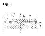
- There has been known a method wherein a full reflection layer is utilized in place of the semi-reflection layer, and that the full reflection layer has openings formed in some portions thereof. This method will be explained, referring to Fig. 3. A
full reflection layer 2 is deposited on one of thesubstrates 1 forming a liquid crystal display, the full reflection layer has some portions removed so as to formlight transmission portions 2a andlight reflection portions 2b by etching, andcolor filters 3 are provided on the light transmission portions and the light reflection portions. - When the display is in a dark place, a bright image is obtained by turning on the backlight and using light irradiated through the
light transmission portions 2a. When the display is in a light place, a bright image is obtained by external light reflected by thelight reflection portions 2b made of thefull reflection layer 2. - In the case of utilizing the
full reflection layer 2 having thelight transmission portions 2a partly formed therein, when the color reproduction properties are set to meet the requirements for thelight reflection portions 2b at the time of providing the color filters, the color purity at thelight transmission portions 2a degrades because of designing for reflection, which gives importance to brightness. On the other hand, when the color reproduction properties are set to meet thelight transmission portions 2a at the time of providing the color filters, thelight reflection portions 2b havea darker image because of designing for transmission, which gives importance to color purity. - Although one of the methods to solve this problem is that color filters are differently applied for transmission and reflection, this method needs to have different steps to provide the color filters, which is unfavorable in terms of costs.
- There is a proposal wherein each of the
color filters 3 is formed to have portions having different thicknesses by providing thefull reflection layer 2 with a greater thickness to form a sufficient stepwise difference between alight transmission portion 2a and its adjacentlight reflection portion 2b so that the light passing through thecolor filters 3 has substantially the same path length on either of transmission and reflection to obtain both transmission properties and reflection properties in a good fashion. However, this is not a favorable method since there is a possibility that a problem of peeling is created since stress increases by increasing the thickness of thefull reflection layer 2, which is normally around 0.2 µm. - There has been known another method wherein the light passing through the color filters has substantially the same path length on either of transmission and reflection by providing a reflection film on each of projected portions of an indented surface of a light diffusion layer and by forming a hole in each of the recessed portions at the time of providing color filters on the uneven surface. However, this method is not practical since the method needs an extremely precise lithographic technique.
- It is an object of the present invention to provide an economical and practical solution capable of realizing good color purity and brightness on both light transmission and light reflection in a transflective color liquid crystal display wherein a full reflection layer is utilized.
- In order to solve the object, according to a first aspect of the present invention, there is provided a transflective color liquid crystal display, wherein one of transparent substrates has an inner surface formed with light reflection portions made of a full reflection layer and light transmission portions formed as openings without the full reflection layer, and wherein a color filter is provided on each paired light reflection portion and light transmission portion, characterized in that the full reflection film has a transparent resist having a thickness provided thereon, and the light transmission portions are formed as holes having a certain depth, whereby the color filters have a greater thickness at the light transmission portions than at the light reflection portions.
- In this case, when the color filters have a 2 times greater thickness at the light transmission portions than at the light reflection portions, the path length of light that passes through the color filters on light transmission becomes equal to the path length of light that passes in the color filters on light reflection. However, it is preferable in terms of compatibility of the color purity on light transmission and the brightness on light reflection that the magnification is set at a value from 1.2 to 4.5 times, preferably from 2.2 to 4.5 times.
- According to a second aspect of the present invention, there is provided a method for fabricating a substrate for a transflective color liquid crystal display, comprising providing one of substrates with light reflection portions made of a full reflection layer and light transmission portions formed as openings without the full reflection layer, and providing a color filter on each paired light reflection portion and light transmission portion, characterized in that the method further comprises providing a transparent resist made of a photosensitive resin only at the light reflection portions by a lithographic technique and firing the transparent resin before provision of the color filter on each paired light reflection portion and light transmission portion.
- In accordance with the method of the present invention, the transparent resist, which is provided on the light reflection portions and made of a photosensitive resist, can be utilized as a stepwise arrangement in order that the color filters have a greater thickness at the light transmission portions than at the light reflection portions. As a result, different color filters do not need to be applied at the light transmission portions and the light reflection portions, reducing loads in the designing process and the fabricating process.
- In drawings:
- Fig. 1 is an enlarged cross-sectional view showing the essential parts of an embodiment of a rear side substrate, which is included in the transflective color liquid crystal display according to the present invention;
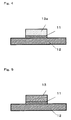
- Fig. 2 is an enlarged cross-sectional view of the essential parts to explain a method for fabricating the rear side substrate;
- Fig. 3 is a cross-sectional view showing the arrangement of a conventional color filter;
- Fig. 4 is a cross-sectional view showing the step in which a photosensitive resin 13a is disposed; and
- Fig. 5 is a cross-sectional view showing the step in
which a
transparent resist 13 is made by baking. -
- In general, a liquid crystal display basically includes a pair of transparent substrates, i.e., a substrate on a viewer side and a substrate on a rear side (a side opposite to the viewer side). For explanation of an embodiment according to the present invention, an arrangement of three pixels (R, G and B) of the
substrate 10 on the rear side, which is used as one of the substrates, is shown in enlargement in Fig. 1. In explanation of the present invention, the substrate on the viewer side as the other substrate is not shown in the accompanying drawings since the viewer side substrate includes no characteristic elements. - The
rear side substrate 10 may be a glass or plastic substrate. The rear side substrate has an inner surface (a surface facing the unshown viewer side substrate) provided with the respective pixels, each of which includes alight reflection portion 11 made of afull reflection layer 11a and alight transmission portion 12 as an opening formed by removing a portion of the full reflection layer by, e.g., etching. - Each
light reflection portion 11 has atransparent resist 13 formed on thefull reflection layer 11a so as to have a certain thickness. Thetransparent resist 13 has a much greater thickness than thefull reflection layer 11a, thereby providing thelight transmission portion 12 with a hole having a length substantially equal to the thickness of thetransparent resist 13. - Although the
light reflection portion 11 and thelight transmission portion 12 have acolor filter 14 with a flat and smooth surface in each of the pixels of R, G and B, thecolor filter 14 has a smaller thickness at thelight reflection portion 11 and a greater thickness at thelight transmission portion 12 since thelight reflection portion 11 has thetransparent resist 13 formed thereon. - Incoming ambient external light is reflected by each
light reflection portion 11, and light that is irradiated from an unshown backlight passes through eachlight transmission portion 12. In that case, the reflected light contributes to produce a bright image since eachcolor filter 14 is thin at the reflection portion. Additionally, the transmission light contributes to produce an image with good color purity since eachcolor filter 14 is thick at the transmission portion. - In order that the brightness on light reflection and the color purity on light transmission are compatible, it is preferable that the
transparent resist 13 has a thickness set so that the thickness of thecolor filter 14 at thelight transmission portions 12 is 1.2 times to 4.5 times the thickness of thecolor filter 14 at thelight reflection portions 11. - Now, referring to Fig. 2, a preferable method for fabricating the
rear side substrate 10 will be described. A transparent substrate, which is made of, e.g., glass, has afull reflection layer 11a deposited on one side working as the inner surface, the transparent substrate with the full reflection layer deposited thereon has a photoresist applied thereon, the photoresist is exposed through a photomask having a pattern for forming light transmission portions, and the exposed photoresist is developed to expose desired portions of the full reflection layer. After the portions of thefull reflection layer 11a to work as the light transmission portions are removed by etching, the unnecessary photoresist is removed. - After the transparent substrate has had the
light reflection portions 11 and thelight transmission portions 12 formed thereon in that manner, the transparent substrate has a transparent positive photosensitive resin 13a applied at a certain thickness so as to have a flat surface (see Fig. 4). The resin is exposed and developed from the other side (rear side) of the substrate, using thefull reflection film 11a at each of the light reflection portions as a photomask. - Since the exposed portions of the positive photosensitive resin are dissolvent, the resin at the
light transmission portions 12 is removed by the developing step. The remaining positive photosensitive resin 13a is baked to form thetransparent resist 13 at each of the light reflection portions (see Fig. 5). After that, acolor filter 14 is provided on each pairedlight reflection portion 11 andlight transmission portion 12 in each pixel. Thus, in accordance with the method of the present invention, it is possible to form thetransparent resist 13 without using a photomask. - Although the photoresist used for patterning the full reflection layer is once removed to avoid an adverse effect given by the patterning step in the embodiment stated earlier, the photoresist used for this patterning step may be utilized as the
transparent photoresist 13 for forming a stepwise arrangement without being removed. In the latter case, the process is further simplified. - Although not shown, the
rear side substrate 10 preferably has a smoothed layer formed on thecolor filters 14 prior to provision of transparent electrodes and an alignment layer. The other substrate as the viewer side substrate also has transparent electrodes and an alignment layer provided on an inner surface, therear side substrate 10 and the viewer side substrate are press-fitted each other through an edge sealant, and the cell gap thus formed has a liquid crystal, such as TN and STN, sealed therein, providing a transflective color liquid crystal display. - A full reflection mirror (full reflection film) was deposited on glass substrates, a photoresist was applied on the glass substrates for mirror patterning, the photoresist was exposed and developed so as to provide targeted portions with light transmission portions, the Ag mirror at the light transmission portions was removed by etching, and the unnecessary photoresist was removed.
- After the light transmission portions were partly provided in the full reflection mirror of each of the glass substrates as stated earlier, a positive photosensitive resist manufactured under the name of PC403 by JSR Corporation as the transparent positive photosensitive resin was applied on the glass substrates at different thicknesses. The resist was wholly exposed from the rear side of each of the substrates, using the mirrors left at the light reflection portions as photomasks. The substrates were prepared so as to have the light transmission portions formed with holes having a depth 1.0 µm, a depth of 2.0 µm and a depth of 3.0 µm, respectively, by developing the resist.
- Then, color filter materials (commercially available under the names of PERR0402, REGG0402 and REBB0402 by Mitsubishi Chemical Corporation) were applied to the respective substrates, preparing color filters, the thicknesses of which are all set at 1.0 µm at the light reflection portions, and the thicknesses of which are respectively set at 1.2 µm, 2.0 µm, 3.0 µm and 4.0 µm at the light transmission portions.
- After that, smoothed layers, transparent row electrodes and alignment layers were provided in this order as in an ordinary liquid crystal display, and paired substrates with the transparent column electrodes and the alignment layers were press-fitted each other through edge sealants, fabricating transflective color liquid crystal displays.
- The light transmission portion of each color filter is 30 µm x 270 µm size, which corresponds to 90 µm width column electrode and 270 µm width row electrode line of passive matrix display.
- In each of the displays, the area of the color gamut at the light reflection portions is calculated as 30. As the thickness increases, the area of the color gamut is calculated as increasing to 14, 30, 50 and 67, and the transmission rate is calculated as lowering to 58%, 48%, 41% and 36%.
- As explained above, in accordance with the present invention, it is possible to realize good color purity and brightness on both light transmission and light reflection by providing the transparent resist having a certain thickness on the full reflection layer at the light reflection portions and forming the light transmission portions as the holes having a certain length in order to provide the color filters with different thicknesses at the light reflection portions and the light transmission portions, when one of the substrates has the inner surface provided with the light reflection portions made of the full reflection layer and the light transmission portions formed as openings without the full reflection layer, and each color filter is provided on each paired light reflection portion and light transmission portion.
- The entire disclosure of Japanese Patent Application No. 2001-335206 filed on October 31, 2001 including specification, claims, drawings and summary is incorporated herein by reference in its entirety.
Claims (11)
- A transflective color liquid crystal display, wherein one of transparent substrates has an inner surface formed with light reflection portions made of a full reflection layer and light transmission portions formed as openings without the full reflection layer, and wherein a color filter is provided on each paired light reflection portion and light transmission portion,
the full reflection layer having a transparent resist provided thereon so as to have a thickness, and the light transmission portions being formed as holes having a depth, whereby the color filters have a greater thickness at the light transmission portions than at the light reflection portions. - The liquid crystal display according to Claim 1, wherein the color filters have a 1.2 to 4.5 times greater thickness at the light transmission portions than at the light reflection portions.
- The liquid crystal display according to Claim 1,
wherein the color filters have 2.2 to 4.5 times greater thickness at the light transmission portions than at the light reflection portions. - The liquid crystal display according to anyone of claims 1 to 3,
wherein TN liquid crystal layer is arranged. - The liquid crystal display according to anyone of claims 1 to 3, wherein STN liquid crystal layer is arranged.
- The liquid crystal display according to anyone of claims 1 to 5, wherein said color filter is used for R, G and B colors.
- The liquid crystal display according to anyone of claims 1 to 6, wherein R, G and B color filters for a pixel is arranged for a row electrode line.
- The liquid crystal display according to anyone of claims 1 to 7, wherein said color filter has a rectangle in a substrate plane.
- The liquid crystal display according to Claim 8, wherein a shorter side of a light transmission portion of said rectangle is equal to or less than 50 µm.
- The liquid crystal display according to anyone of claims 1 to 9, wherein Ag is used for said reflection layer.
- A method for fabricating a substrate for a transflective color liquid crystal display, comprising providing one of substrates with light reflection portions made of a full reflection layer and light transmission portions formed as openings without the full reflection layer, and providing a color filter on each paired light reflection portion and light transmission portion,
the method further comprising providing a transparent resist made of a photosensitive resin only at the light reflection portions by a lithographic technique and baking the transparent resin before provision of the color filter on each paired light reflection portion and light transmission portion.
Applications Claiming Priority (2)
| Application Number | Priority Date | Filing Date | Title |
|---|---|---|---|
| JP2001335206 | 2001-10-31 | ||
| JP2001335206 | 2001-10-31 |
Publications (2)
| Publication Number | Publication Date |
|---|---|
| EP1312973A2 true EP1312973A2 (en) | 2003-05-21 |
| EP1312973A3 EP1312973A3 (en) | 2004-02-11 |
Family
ID=19150218
Family Applications (1)
| Application Number | Title | Priority Date | Filing Date |
|---|---|---|---|
| EP02023751A Withdrawn EP1312973A3 (en) | 2001-10-31 | 2002-10-24 | Transflective color liquid crystal display and method for fabricating a substrate therefor |
Country Status (5)
| Country | Link |
|---|---|
| US (1) | US7158198B2 (en) |
| EP (1) | EP1312973A3 (en) |
| KR (1) | KR20030036058A (en) |
| CN (1) | CN1417626A (en) |
| TW (1) | TWI224696B (en) |
Families Citing this family (8)
| Publication number | Priority date | Publication date | Assignee | Title |
|---|---|---|---|---|
| JP4023470B2 (en) * | 2003-07-29 | 2007-12-19 | セイコーエプソン株式会社 | Electro-optical device, substrate for electro-optical device, electronic apparatus, and method for manufacturing electro-optical device |
| JP4663302B2 (en) * | 2004-11-26 | 2011-04-06 | 京セラ株式会社 | Liquid crystal display device and display body using the same |
| US20060132678A1 (en) * | 2004-12-17 | 2006-06-22 | Sharp Kabushiki Kaisha | Color filter substrate and liquid crystal display device |
| CN102262351B (en) * | 2010-05-25 | 2013-01-23 | 无锡华润上华半导体有限公司 | Photomask layer and its formation method |
| CN102707355A (en) | 2011-10-24 | 2012-10-03 | 京东方科技集团股份有限公司 | Transreflective color filter and manufacturing method thereof |
| TWI507742B (en) | 2013-11-26 | 2015-11-11 | E Ink Holdings Inc | Color filter substrate and display device |
| JP6854898B2 (en) * | 2016-12-30 | 2021-04-07 | トンシュー(クンシャン) ディスプレイ マテリアル カンパニー リミテッドTunghsu (Kunshan) Display Material Co., Ltd. | Manufacturing method of color filter, display device and color filter |
| CN115236895B (en) * | 2022-09-23 | 2023-01-20 | 合肥泰沃达智能装备有限公司 | Double-layer reflection and light transmission type reflection screen and preparation method thereof |
Citations (3)
| Publication number | Priority date | Publication date | Assignee | Title |
|---|---|---|---|---|
| JPH0611711A (en) * | 1992-06-26 | 1994-01-21 | Sharp Corp | Reflection type liquid crystal display device |
| JPH1152366A (en) * | 1997-08-04 | 1999-02-26 | Toppan Printing Co Ltd | Translucent type liquid crystal display device |
| JP2000298271A (en) * | 1999-04-13 | 2000-10-24 | Matsushita Electric Ind Co Ltd | Liquid crystal display device and production therefor |
Family Cites Families (7)
| Publication number | Priority date | Publication date | Assignee | Title |
|---|---|---|---|---|
| EP0576303B1 (en) * | 1992-06-26 | 1998-10-14 | Sharp Kabushiki Kaisha | Reflective type liquid crystal display device |
| KR100681764B1 (en) * | 1999-12-06 | 2007-02-15 | 엘지.필립스 엘시디 주식회사 | Transflective liquid crystal display device |
| KR100661825B1 (en) * | 1999-12-28 | 2006-12-27 | 엘지.필립스 엘시디 주식회사 | Array substrate of transflective liquid crystal display device and method for fabricating the same |
| KR100603846B1 (en) * | 2000-02-10 | 2006-07-24 | 엘지.필립스 엘시디 주식회사 | transflective liquid crystal display device |
| US6690438B2 (en) * | 2001-04-06 | 2004-02-10 | Citizen Watch Co., Ltd. | Liquid crystal display panel |
| JP3644442B2 (en) * | 2001-08-07 | 2005-04-27 | セイコーエプソン株式会社 | Color filter substrate and manufacturing method thereof, liquid crystal display device and manufacturing method thereof, and electronic apparatus |
| JP4264217B2 (en) * | 2001-09-25 | 2009-05-13 | シャープ株式会社 | Substrate with colored layer |
-
2002
- 2002-10-24 EP EP02023751A patent/EP1312973A3/en not_active Withdrawn
- 2002-10-24 TW TW091124782A patent/TWI224696B/en not_active IP Right Cessation
- 2002-10-28 US US10/281,108 patent/US7158198B2/en not_active Expired - Lifetime
- 2002-10-30 KR KR1020020066589A patent/KR20030036058A/en not_active Application Discontinuation
- 2002-10-31 CN CN02148272A patent/CN1417626A/en active Pending
Patent Citations (3)
| Publication number | Priority date | Publication date | Assignee | Title |
|---|---|---|---|---|
| JPH0611711A (en) * | 1992-06-26 | 1994-01-21 | Sharp Corp | Reflection type liquid crystal display device |
| JPH1152366A (en) * | 1997-08-04 | 1999-02-26 | Toppan Printing Co Ltd | Translucent type liquid crystal display device |
| JP2000298271A (en) * | 1999-04-13 | 2000-10-24 | Matsushita Electric Ind Co Ltd | Liquid crystal display device and production therefor |
Non-Patent Citations (3)
| Title |
|---|
| PATENT ABSTRACTS OF JAPAN vol. 018, no. 211 (P-1726), 14 April 1994 (1994-04-14) -& JP 06 011711 A (SHARP CORP), 21 January 1994 (1994-01-21) -& EP 0 576 303 A (SHARP KK) 29 December 1993 (1993-12-29) * |
| PATENT ABSTRACTS OF JAPAN vol. 1999, no. 05, 31 May 1999 (1999-05-31) & JP 11 052366 A (TOPPAN PRINTING CO LTD), 26 February 1999 (1999-02-26) * |
| PATENT ABSTRACTS OF JAPAN vol. 2000, no. 13, 5 February 2001 (2001-02-05) -& JP 2000 298271 A (MATSUSHITA ELECTRIC IND CO LTD), 24 October 2000 (2000-10-24) * |
Also Published As
| Publication number | Publication date |
|---|---|
| US7158198B2 (en) | 2007-01-02 |
| KR20030036058A (en) | 2003-05-09 |
| EP1312973A3 (en) | 2004-02-11 |
| TWI224696B (en) | 2004-12-01 |
| US20030090610A1 (en) | 2003-05-15 |
| CN1417626A (en) | 2003-05-14 |
Similar Documents
| Publication | Publication Date | Title |
|---|---|---|
| KR101113115B1 (en) | Liquid crystal display device and display equipment using the same | |
| JP3032197B1 (en) | Color filter and optical display | |
| US20150253473A1 (en) | Color filter array substrate, method for fabricating the same and display device | |
| US6704075B2 (en) | Color filter substrate, method of fabricating color filter substrate, liquid crystal device, method of fabricating liquid crystal device, and electronic apparatus | |
| US20070182889A1 (en) | Liquid crystal display device and method for manufacturing the same | |
| US6323920B1 (en) | Methods of making LCD devices having color filter | |
| JP2000162625A (en) | Color reflection type liquid crystal display device and its production | |
| US20060028599A1 (en) | Color liquid crystal display device and method of manufacturing the same, and method of manufacturing a color filter substrate | |
| US6037084A (en) | Method of making a color filter plate with multi-gap for LCD | |
| US7158198B2 (en) | Transflective color liquid crystal display including color filters on transparent resists and method of fabricating a substrate therefor | |
| US7102716B2 (en) | LCD with TFT on upper substrate and color filter on each substrate | |
| KR20010007310A (en) | Liquid crystal display device and method for fabricating the same | |
| JP2002236210A (en) | Method for manufacturing color filter | |
| JP2002341333A (en) | Translucent liquid crystal display device and manufacturing method therefor | |
| JP2000098128A (en) | Color filter | |
| JP4864895B2 (en) | Transflective display device | |
| JP4663302B2 (en) | Liquid crystal display device and display body using the same | |
| KR100430948B1 (en) | A color filter for transflective LCD and method for fabricating thereof | |
| JP3234150B2 (en) | Color display | |
| KR20030056246A (en) | Color filter including a scattering layer for a liquid crystal display and a manufacturing method thereof | |
| KR20010004912A (en) | Color filter structure in LCD and method for manufacturing the same | |
| JP2004045782A (en) | Color liquid crystal device | |
| KR20050079813A (en) | Color filter substrate and manufacturing method thereof | |
| KR20050091981A (en) | Color filter substrate, method of manufacturing the same and liquid crystal display apparatus having the same | |
| JPH10161104A (en) | Color liquid crystal display element and its manufacture |
Legal Events
| Date | Code | Title | Description |
|---|---|---|---|
| PUAI | Public reference made under article 153(3) epc to a published international application that has entered the european phase |
Free format text: ORIGINAL CODE: 0009012 |
|
| AK | Designated contracting states |
Designated state(s): AT BE BG CH CY CZ DE DK EE ES FI FR GB GR IE IT LI LU MC NL PT SE SK TR |
|
| AX | Request for extension of the european patent |
Extension state: AL LT LV MK RO SI |
|
| PUAL | Search report despatched |
Free format text: ORIGINAL CODE: 0009013 |
|
| AK | Designated contracting states |
Kind code of ref document: A3 Designated state(s): AT BE BG CH CY CZ DE DK EE ES FI FR GB GR IE IT LI LU MC NL PT SE SK TR |
|
| AX | Request for extension of the european patent |
Extension state: AL LT LV MK RO SI |
|
| 17P | Request for examination filed |
Effective date: 20040304 |
|
| AKX | Designation fees paid |
Designated state(s): DE FR GB |
|
| 17Q | First examination report despatched |
Effective date: 20050221 |
|
| STAA | Information on the status of an ep patent application or granted ep patent |
Free format text: STATUS: THE APPLICATION IS DEEMED TO BE WITHDRAWN |
|
| 18D | Application deemed to be withdrawn |
Effective date: 20050705 |