EP1312907A1 - Pressure detecting apparatus - Google Patents
Pressure detecting apparatus Download PDFInfo
- Publication number
- EP1312907A1 EP1312907A1 EP02006550A EP02006550A EP1312907A1 EP 1312907 A1 EP1312907 A1 EP 1312907A1 EP 02006550 A EP02006550 A EP 02006550A EP 02006550 A EP02006550 A EP 02006550A EP 1312907 A1 EP1312907 A1 EP 1312907A1
- Authority
- EP
- European Patent Office
- Prior art keywords
- external case
- opening
- sensor unit
- lead material
- resin
- Prior art date
- Legal status (The legal status is an assumption and is not a legal conclusion. Google has not performed a legal analysis and makes no representation as to the accuracy of the status listed.)
- Withdrawn
Links
Images


Classifications
-
- G—PHYSICS
- G01—MEASURING; TESTING
- G01L—MEASURING FORCE, STRESS, TORQUE, WORK, MECHANICAL POWER, MECHANICAL EFFICIENCY, OR FLUID PRESSURE
- G01L19/00—Details of, or accessories for, apparatus for measuring steady or quasi-steady pressure of a fluent medium insofar as such details or accessories are not special to particular types of pressure gauges
- G01L19/14—Housings
-
- G—PHYSICS
- G01—MEASURING; TESTING
- G01L—MEASURING FORCE, STRESS, TORQUE, WORK, MECHANICAL POWER, MECHANICAL EFFICIENCY, OR FLUID PRESSURE
- G01L19/00—Details of, or accessories for, apparatus for measuring steady or quasi-steady pressure of a fluent medium insofar as such details or accessories are not special to particular types of pressure gauges
- G01L19/14—Housings
- G01L19/147—Details about the mounting of the sensor to support or covering means
-
- G—PHYSICS
- G01—MEASURING; TESTING
- G01L—MEASURING FORCE, STRESS, TORQUE, WORK, MECHANICAL POWER, MECHANICAL EFFICIENCY, OR FLUID PRESSURE
- G01L19/00—Details of, or accessories for, apparatus for measuring steady or quasi-steady pressure of a fluent medium insofar as such details or accessories are not special to particular types of pressure gauges
- G01L19/0007—Fluidic connecting means
- G01L19/0038—Fluidic connecting means being part of the housing
-
- G—PHYSICS
- G01—MEASURING; TESTING
- G01L—MEASURING FORCE, STRESS, TORQUE, WORK, MECHANICAL POWER, MECHANICAL EFFICIENCY, OR FLUID PRESSURE
- G01L19/00—Details of, or accessories for, apparatus for measuring steady or quasi-steady pressure of a fluent medium insofar as such details or accessories are not special to particular types of pressure gauges
- G01L19/0061—Electrical connection means
- G01L19/0084—Electrical connection means to the outside of the housing
-
- G—PHYSICS
- G01—MEASURING; TESTING
- G01L—MEASURING FORCE, STRESS, TORQUE, WORK, MECHANICAL POWER, MECHANICAL EFFICIENCY, OR FLUID PRESSURE
- G01L19/00—Details of, or accessories for, apparatus for measuring steady or quasi-steady pressure of a fluent medium insofar as such details or accessories are not special to particular types of pressure gauges
- G01L19/14—Housings
- G01L19/148—Details about the circuit board integration, e.g. integrated with the diaphragm surface or encapsulation
Definitions
- the present invention relates to a pressure detecting apparatus and more particularly to a pressure detecting apparatus mounting electronic parts for reducing electric disturbance.
- a conventional pressure detecting apparatus for example, as described in Japanese Application Patent Laid-open Publication no. Hei 10-170380, is a 2-chip sensor unit composed of a semiconductor sensor chip for converting a physical quantity to an electric signal and a semiconductor circuit chip for carrying out operations for a sensor output signal and obtaining a detection signal.
- the 2-chip constitution is a structure that the aforementioned semiconductor circuit chip is arranged on the lead frame, sealed with resin, thereby constitutes a package partially having a cavity, and the sensor unit that the semiconductor sensor chip is arranged in the cavity and electrically connected is arranged in the concave opening of the external case which is formed integratedly with the lead material having the concave opening and partially the connector terminal which is partially exposed into the concave opening, and the lead material is electrically joined with the lead frame, and then the package is closed with the cover.
- the present invention is intended to provide a pressure detecting apparatus capable of easily responding to specification changes.
- the present invention has a lead material partially having a connector terminal for electrical connection with the outside, an external case partially having an opening which is formed integratedly with the lead material, a sensor unit composed of a semiconductor sensor for converting pressure to an electric signal, a signal processing circuit, an output terminal for outputting the processed signal, and a chip case partially having an opening as main component parts, and an electronic part for reducing electric disturbance, and a part of the lead material is exposed into the opening of the external case, and the sensor unit and electronic part are arranged in the opening of the external case, and the lead material, electronic part, and terminal of the sensor unit are electrically connected to each other in the opening of the external case.
- the present invention can easily respond to specification changes.
- the external case is provided with a pressure introduction hole interconnecting with the opening of the external case, and the opening of the sensor unit and the opening of the external case are respectively provided with fitting parts, and the sensor unit and external case are fit into each other so that the semiconductor sensor of the sensor unit and the air introduction hole of the external case are interconnected with each other, and the sensor unit, electronic part, and exposed part of the lead material which are arranged in the opening of the external case are covered overall or partially with resin injected into the opening of the external case and integratedly fixed with injected resin, and the fitting part of the sensor unit and external case is sealed airtightly.
- the present invention has a lead material partially having a connector terminal for electrical connection with the outside, an external case partially having an opening and a pressure introduction hole interconnecting with the opening which is formed integratedly with the lead material, and a sensor unit composed of a semiconductor sensor for converting pressure to an electric signal, a signal processing circuit, an output terminal for outputting the processed signal, and a chip case partially having an opening as main component parts, and a part of the lead material is exposed into the opening of the external case, and the opening of the sensor unit is arranged in the opening of the external case so as to interconnect with the pressure introduction hole, and the lead material and output terminal of the sensor unit are electrically connected in the opening of the external case, and the sensor unit and exposed part of the lead material arranged in the opening of the external case are covered overall or partially with resin injected into the opening of the external case, and the sensor unit and external case are integratedly fixed with the injected resin.
- the present invention can easily respond to specification changes.
- the semiconductor sensor of the sensor unit is an absolute pressure sensor having a reference pressure chamber, and the semiconductor sensor for converting the pressure of the sensor unit to an electric signal and the signal processing circuit are composed of one chip, and the electronic part is composed of chip parts such as a capacitor and a resistor, and the external case is composed of thermoplastic resin, and resin to be injected into the opening of the external case is composed of thermoset resin, and the coefficients of linear expansion of the aforementioned thermoplastic resin and thermoset resin are set within the range from 20 to 40 ppm/°C.
- the output terminal of the sensor unit and the lead material of the external case are electrically connected by welding, and a hollow is formed in the electronic part arrangement portion of the lead material, and a partition or groove for separating the hollows of different lead materials is formed in the external case, and the electrode parts of the electronic parts arranged in the hollows of the lead material are electrically connected with a junction member.
- the welding electrode arrangement area between the lead material of the external case and the output terminal of the sensor unit and the electronic part arrangement area are separated from each other without coexisting.
- the lead materials to be extended across are bent in a crank shape and embedded in the resin of the external case or the lead materials to be extended across are made thinner, and the electronic part arrangement portion of the lead materials is partially made wider.
- the end face of the opening of the sensor unit and the arrangement surface of the output terminal are different from each other and on at least one part between the contact surface with the end face of the opening of the sensor unit of the external case and the arrangement surface of the lead material electrically joined to the output terminal, an inclined surface is provided.
- a cover having a fitting part into the sensor unit or a part of the external case which is arranged so as to block the opening of the external case overall or partially is provided and the cover, sensor unit, and external case are integratedly fixed with injected resin.
- Fig. 1 is a cross sectional view of the pressure detecting apparatus of the first embodiment of the present invention.
- Fig. 2 is a front view of the pressure detecting apparatus of the first embodiment of the present invention.
- a semiconductor sensor chip 1 is composed of silicon.
- a concavity is formed on the lower surface of the center part of the semiconductor sensor chip 1 by etching and a thin diaphragm 2 is formed at the center part.
- a pressure detection circuit not shown in the drawing is integratedly formed by the semiconductor process.
- the pressure detection circuit is composed of four diffused resistors formed on the upper surface of the diaphragm 2 and they are bridged by aluminum conductors.
- the characteristic compensation circuit is composed of a digital-analog mixed circuit for adjusting the relation between pressure and output to a predetermined transfer function.
- the digital-analog mixed circuit is composed of a digital unit having an EPROM for storing and holding a characteristic adjustment signal and an analog unit for amplifying a signal as main units.
- the characteristic adjustment signal is used to adjust each characteristic obtained by zero-span adjustment, sensitivity adjustment, and temperature characteristic adjustment.
- the protection circuit is a circuit installed at the input-output stage connected with the outside for protecting the internal circuit against transient electromagnetic noise for an input-output signal.
- the pressure detection circuit, characteristic adjustment circuit, and protection circuit are electrically connected respectively with aluminum conductors.
- the semiconductor sensor chip 1 is joined to a glass base 3 with Anodic Bonding.
- the semiconductor sensor chip 1 and the glass base 3 constitute a chip assembly.
- a reference pressure chamber 4 which is almost evacuated is installed.
- the linear expansion coefficient of the glass base 3 is structured so as to be almost equal to the linear expansion coefficient of the semiconductor chip 1.
- a chip case 5 is composed of thermoset resin such as epoxy resin or thermoplastic resin such as PPS and a terminal 6 is composed of phosphor bronze.
- the terminal 6 is obtained by pressing a hoop material pre-plated with nickel into shapes and the chip case 5 with a terminal is structured by insert molding using epoxy resin. After the chip case is molded, the terminal is connected in a rectangular shape, though 5 adjustment terminals and 3 input-output terminals are cut off so that the respective terminals become independent.
- a concave chip assembly storage unit 7 is installed on the bottom of the chip case 5 on the opening side.
- the terminal 6 is arranged so that a part thereof is exposed in the periphery of the arrangement portion of the chip assembly and a part thereof is pulled out from the chip case 5.
- the chip assembly composed of the semiconductor sensor chip 1 and the glass base 3 is adhered and fixed to the concavity 7 of the chip case 5 with an silicon series adhesive 8.
- the electrode of the semiconductor sensor chip 1 is wire-bonded to the terminal 6 with a wire 9 composed of gold or aluminum.
- the chip assembly composed of the semiconductor sensor chip 1 and the glass base 3 which is arranged on the chip case 5, the aluminum wire 9, and the exposed part of the lead terminal 6 are covered with a silicone gel 10 of phlorosilicon series or fluorine series.
- the silicone gel 10 prevents transfer of pressure to the semiconductor chip 1 and contact with a corrosive liquid and gas.
- a sensor unit 11 is structured as mentioned above.
- the sensor unit 11 brings a probe into contact with the adjustment terminal and the input-output terminal 12 and electrically communicates with the external pressure adjustment device, thereby adjusts the characteristics of the inner circuit of the semiconductor sensor chip, and then cuts off the parts of the adjustment terminal and the input-output terminal 12 which are projected outside the case to predetermined lengths.
- a lead material 13 is composed of brass.
- the lead material is formed by pressing a hoop material pre-plated with tin.
- the right side of the lead material on the paper sheet is pressed to a shape of a connector terminal 14 and the left side thereof is pressed to a shape of a terminal 15 bent almost perpendicularly to the connector terminal 14.
- a welding projection 16 is installed at the position where the input-output terminal 12 of the sensor unit 11 is welded.
- the lead material 13 is composed of a ground terminal 17, an output terminal 18, and a power terminal 19 sequentially from the upper side of the paper sheet of Fig. 2. In the neighborhood of the center between the ground terminal 17 and the output terminal 18, an almost rectangular hollow 20 for arranging the chip capacitor is formed.
- the depth of the hollow of the lead material is preferably about 1/3 to 1/2 of the thickness of the lead material 13 and the size of the almost rectangular bottom of the hollow is preferably a size almost equal to the arrangement shape of the chip capacitor electrode.
- an almost rectangular hollow for arranging the chip capacitor must be formed in the ground terminal 17 and the power terminal 19.
- the output terminal 18 lies between both terminals, so that a wide terminal 21 is installed in the neighborhood of the chip capacitor arrangement portion of the ground terminal 17 and the power terminal 19 and a hollow 22 is formed in the neighborhood of the end thereof.
- An external case 23 is obtained by insert-molding the lead material 13.
- the lead material 13 of the external case 23 is fixed to the mold by the two faces of an exposed part 24 in the opening and an exposed part 25 in the perpendicular direction to it at the time of insert molding. Therefore, a lead material fixing pin for injection molding is not required, so that the mold cost can be decreased. Furthermore, the trace of the press pin running from the back of the lead material to the outside of the external case is eliminated, so that the air-tightness of the external case is increased.
- the external case 23 is composed of thermoplastic PPS resin.
- the external case 23 is injected by a predetermined mold, thus a connector coupler 26, a flange 27, an opening 28, a pressure introduction pipe 30 having a pressure introduction hole 29 interconnecting with the opening, and a convex fitting part 31 formed in the opening are installed. Further, an inclined surface 33 for connecting an inner arrangement surface 32 of the opening of the sensor unit 11 and the exposed surface 24 of the lead material on the connector coupler side is installed and on the resin portion between the different lead materials of the exposed part 24 of the lead material, an inclined surface is also installed.
- the input-output terminal 12 of the sensor unit 11 is overlaid on the welding projection 16 installed on the exposed part 30 of the lead material.
- the welding projection 16 of the lead material and the input-output terminal 12 of the sensor unit are electrically joined using projection welding.
- the lead material of the external case and the sensor unit terminal are welded by supplying a current between the electrode arranged on the welding projection 16 and the electrode arranged in a welding electrode position 34.
- the loading part of chip capacitors 36 and 37 of the lead material 13 is a different area from the welding current path of the lead material 13 and terminal, so that no failure is generated in tin plating fusion of the lead material of the chip capacitor loading part and resin fusion in the neighborhood of the lead material and the lead material and peripheral resin can load the chip capacitor in a predetermined shape, so that high connection reliability and production yield can be obtained.
- the chip capacitors 36 and 37 having electrodes at both ends are arranged.
- the hollows 20 and 22 of the lead material and the chip capacitor arranged part are almost equal rectangles and have a depth of 1/3 to 1/2 of the thickness of the lead material, so that the chip capacitors 36 and 37 are exactly set in a predetermined position and will not be shifted.
- the external case 23 is preheated at a predetermined temperature and by pressing the upper part of the chip capacitors 36 and 37, the conductive junction member 37 such as string solder is supplied from obliquely aside the chip capacitors 36 and 37.
- the conductive junction member 37 such as string solder is supplied from obliquely aside the chip capacitors 36 and 37.
- string solder is supplied in the neighborhood of the electrodes of the chip capacitors 36 and 37 and the lead material 13
- the solder is fused by irradiating a laser beam and both members are electrically joined.
- the inclined surface 33 for connecting the arrangement surface 32 of the sensor unit opening and the arrangement surface of the exposed part 30 of the lead material is installed between the lead materials, so that the resin between the lead materials is also removed in a groove shape. Therefore, the electrically joined member 37 fused between the lead materials and the chip capacitor electrodes will not short between the electrodes of the chip capacitors. Further, when there is another lead material between the arrangement parts of the chip capacitors, the part of the intermediate lead material extending across the chip capacitors is made thinner, and the lead materials on both sides are inversely set in a wider terminal shape 21, and the hollow 22 for loading the chip capacitors are formed in the neighborhood of the ends of the wider parts.
- the resin between the different terminals is removed in a groove shape in the same way as with the aforementioned, so that the conductive joined member 37 coated on the hollow of the lead material will not short between the electrodes of the chip capacitors and between the electrodes and the lead materials. Further, in this case, instead of making the intermediate lead material thinner, even if the part is bent in a crank shape and embedded in the external case, the same effect is obtained.
- the sensor unit 11 and the chip capacitors 36 and 37 are electrically connected to a predetermined position of the lead material 13 of the external case 23, and then by pressing the top of the sensor unit 11, the epoxy resin 37 is injected from the neighborhood of the exposed part 24 of the lead material of the opening 28 of the external case 23, and the resin is set by adding a predetermined temperature, and the sensor unit and external case are fixed strongly.
- the inclined surface 33 provided in the opening of the external case 23 functions so as to deliver the injected resin equally around the sensor unit arrangement part. By doing this, the sensor unit can be kept airtight and surely fixed to the external case, so that improvement of reliability and yield can be obtained.
- the epoxy resin has good fluidity, so that it can fill up a minute gap generated between an insert lead material and resin when insert parts such as lead materials are integratedly formed using thermoplastic resin and an external case is formed, thus no space is left. Therefore, corrosion and disconnection of the junction due to entering of water or corrosive gas into an electrical junction member such as solder or conductive adhesive can be prevented and a problem of poor air-tightness of the insert terminal which is always imposed in thermoplastic PPS resin can be solved. Therefore, after molding, it is not necessary to coat and set an air-tight seal material such as a silicon adhesive on the connector terminal. Further, in this work, evacuated and deaerated epoxy resin is slowly injected in a vacuum, so that finer filling-up free of bubbles can be carried out, so that further improvement of reliability and yield can be obtained.
- thermoplastic PPS resin constituting the external case 23 and the epoxy resin 31 to be injected in the opening of the external case are almost equal in linear expansion coefficient within the range from 20 to 40 ppm/°C, so that separation of the adhesive interface which is always a problem in adhesion of different kinds of materials is not caused.
- the heat shock durability test of -40°C ⁇ 130°C/hour is executed 2000 cycles, no separation is generated on the adhesive interface, and the electrical connection with the chip capacitors 36 and 37 loaded on the lead material 13 is ensured, and an extremely stable mounting structure is obtained.
- this embodiment is structured so as to load a chip capacitor for improving the transient voltage resistance and failure resistance by radio waves in the input-output terminal beforehand, so that the embodiment is structured so as to fully compensate for the flexibility of the chip resistance which is a disadvantage for use of a 1-chip semiconductor sensor and the development expenses and period can be reduced.
- this embodiment does not require parts such as a cover for the opening 28 of the external case 23, so that the embodiment has a mounting structure for greatly contributing to miniaturization of the external case due to abolition of the fitting space between both members and cost reduction due to reduction in the manufacture man-hour.
- a pressure detector that the sensor unit for detecting pressure and an electronic part for reducing electrical disturbance are electrically joined to the lead material of the opening of the external case, and thermoset resin is injected and set in the aforementioned opening, thus the aforementioned members are fixed to each other can be obtained, so that even if the single 1-chip semiconductor sensor may not satisfy the transient voltage resistance and electromagnetic failure resistance, an external electronic part whose performance is compensated for by a method which is inexpensive and has high connection reliability can be mounted and the cost can be reduced by miniaturization, light in weight, and reduction in the assembly man-hour. Therefore, at the time of changing the specification, the embodiment can easily respond to it.
- Fig. 3 is a cross sectional view of the pressure detector of the second embodiment of the present invention.
- the same numerals shown in Figs. 1 and 2 indicate the same parts.
- a cover 39 for the opening 38 of the external case 23 has a fitting part 40 into the upper part of the sensor unit 11 and a resin injection hole 41.
- the sensor unit 11 and the chip capacitors 36 and 37 are electrically joined to the lead material 13, and then the cover 39 is fit into the sensor unit 11, and by pressing the upper part of the cover 39, epoxy resin 38 is injected from the resin injection hole 41.
- the epoxy resin 38 is injected until the resin injection hole 41 of the cover 39 is stopped up and the cover 39, the sensor unit 11, and the external case 23 are simultaneously fixed by adding a predetermined temperature.
- the cover 39 is fit into the sensor unit 11 so as to cover and enclose the outer periphery of the chip case 5, so that the chip case can be isolated from the effect of the shrinkage stress due to injection and setting of the epoxy resin. Therefore, even if the sensor unit 11 is under a specification for main use of minute pressure detection, a stable pressure detector can be obtained.
- the embodiment can easily respond to it.
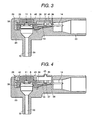
- Fig. 4 is a cross sectional view of the pressure detector of the third embodiment of the present invention.
- the same numerals as those shown in Figs. 1, 2, and 3 indicate the same parts.
- a cover 42 for the opening 38 of the external case 23 has a fitting part 43 into the upper part of the sensor unit 11 and a resin injection hole 44.
- the sensor unit 11 and the chip capacitors 36 and 37 are electrically joined to the lead material 13, and then the cover 42 is fit into the sensor unit 11, and by pressing the upper part of the cover 42, the epoxy resin 38 is injected from the resin injection hole 44.
- the epoxy resin 38 is injected until the chip capacitors 36 and 37 are covered with resin and the peripheral part of the cover 42 inserted in the opening of the external case 23 is filled up with a predetermined amount of injected resin and the cover 39, the sensor unit 11, and the external case 23 are simultaneously fixed by adding a predetermined temperature.
- projected resin around the resin injection hole 44 which is not shown in the drawing is fused by heat caulking so as to form a cap 45 and the opening 28 of the external case 23 is interrupted from the outside.
- the embodiment can easily respond to it.
- Fig. 5 is a cross sectional view of the pressure detector of the fourth embodiment of the present invention.
- the same numerals as those shown in Figs. 1 to 4 indicate the same parts.
- the chip capacitors 36 and 37 shown in Fig. 1 are omitted. Namely, when the performance of the semiconductor sensor chip satisfies the customer required specification, it is not always necessary to arrange the capacitors 36 and 37 on the lead material 13 and the capacitors can be abolished.
- the external case can be miniaturized more and lightweight, reduction in the assembly man-hour, and reduction in the number of parts can be realized.
- the present invention at the time of changing the specification, can easily respond to it.
Landscapes
- Physics & Mathematics (AREA)
- General Physics & Mathematics (AREA)
- Chemical & Material Sciences (AREA)
- Analytical Chemistry (AREA)
- Measuring Fluid Pressure (AREA)
- Structures Or Materials For Encapsulating Or Coating Semiconductor Devices Or Solid State Devices (AREA)
Abstract
The present invention provides a pressure detector capable of easily
responding to changes in the specification. The pressure detector
that the sensor unit (11) for detecting pressure and the electronic
parts (35) and (36) for reducing electrical disturbance are electrically
joined to the exposed part (24) of the lead material (13) of the
opening (28) of the external case (23) and the thermoset resin (38) is
injected and set in the opening (28), thus the members are fixed can
be obtained. An external electronic part for compensating for the
transient voltage resistance and electromagnetic failure resistance of
a single one-chip semiconductor sensor can be mounted and the
cost can be reduced by miniaturization, lightweight, and reduction
in the assembly man-hour.
Description
- The present invention relates to a pressure detecting apparatus and more particularly to a pressure detecting apparatus mounting electronic parts for reducing electric disturbance.
- A conventional pressure detecting apparatus, for example, as described in Japanese Application Patent Laid-open Publication no. Hei 10-170380, is a 2-chip sensor unit composed of a semiconductor sensor chip for converting a physical quantity to an electric signal and a semiconductor circuit chip for carrying out operations for a sensor output signal and obtaining a detection signal. The 2-chip constitution is a structure that the aforementioned semiconductor circuit chip is arranged on the lead frame, sealed with resin, thereby constitutes a package partially having a cavity, and the sensor unit that the semiconductor sensor chip is arranged in the cavity and electrically connected is arranged in the concave opening of the external case which is formed integratedly with the lead material having the concave opening and partially the connector terminal which is partially exposed into the concave opening, and the lead material is electrically joined with the lead frame, and then the package is closed with the cover.
- However, in a conventional sensor unit of 2-chip constitution, when the user-required specification for transient voltage resistance and electromagnetic resistance is graded up more severely, a conventional semiconductor chip may not meet with the specification. If this occurs, it is necessary to re-design a customized chip and respond to it and a problem arises that many man-hours and expenses are required.
- The present invention is intended to provide a pressure detecting apparatus capable of easily responding to specification changes.
- (1) To accomplish the above object, the present invention has a lead material partially having a connector terminal for electrical connection with the outside, an external case partially having an opening which is formed integratedly with the lead material, a sensor unit composed of a semiconductor sensor for converting pressure to an electric signal, a signal processing circuit, an output terminal for outputting the processed signal, and a chip case partially having an opening as main component parts, and an electronic part for reducing electric disturbance, and a part of the lead material is exposed into the opening of the external case, and the sensor unit and electronic part are arranged in the opening of the external case, and the lead material, electronic part, and terminal of the sensor unit are electrically connected to each other in the opening of the external case.
- By use of this constitution, the present invention can easily respond to specification changes.
- (2) In (1) mentioned above, it is preferable that the external case is provided with a pressure introduction hole interconnecting with the opening of the external case, and the opening of the sensor unit and the opening of the external case are respectively provided with fitting parts, and the sensor unit and external case are fit into each other so that the semiconductor sensor of the sensor unit and the air introduction hole of the external case are interconnected with each other, and the sensor unit, electronic part, and exposed part of the lead material which are arranged in the opening of the external case are covered overall or partially with resin injected into the opening of the external case and integratedly fixed with injected resin, and the fitting part of the sensor unit and external case is sealed airtightly.
- (3) To accomplish the above object, the present invention has a lead material partially having a connector terminal for electrical connection with the outside, an external case partially having an opening and a pressure introduction hole interconnecting with the opening which is formed integratedly with the lead material, and a sensor unit composed of a semiconductor sensor for converting pressure to an electric signal, a signal processing circuit, an output terminal for outputting the processed signal, and a chip case partially having an opening as main component parts, and a part of the lead material is exposed into the opening of the external case, and the opening of the sensor unit is arranged in the opening of the external case so as to interconnect with the pressure introduction hole, and the lead material and output terminal of the sensor unit are electrically connected in the opening of the external case, and the sensor unit and exposed part of the lead material arranged in the opening of the external case are covered overall or partially with resin injected into the opening of the external case, and the sensor unit and external case are integratedly fixed with the injected resin.
By use of this constitution, the present invention can easily respond to specification changes. - (4) In (1) or (3) mentioned above, it is preferable that the semiconductor sensor of the sensor unit is an absolute pressure sensor having a reference pressure chamber, and the semiconductor sensor for converting the pressure of the sensor unit to an electric signal and the signal processing circuit are composed of one chip, and the electronic part is composed of chip parts such as a capacitor and a resistor, and the external case is composed of thermoplastic resin, and resin to be injected into the opening of the external case is composed of thermoset resin, and the coefficients of linear expansion of the aforementioned thermoplastic resin and thermoset resin are set within the range from 20 to 40 ppm/°C.
- (5) In (1) or (3) mentioned above, it is preferable that the output terminal of the sensor unit and the lead material of the external case are electrically connected by welding, and a hollow is formed in the electronic part arrangement portion of the lead material, and a partition or groove for separating the hollows of different lead materials is formed in the external case, and the electrode parts of the electronic parts arranged in the hollows of the lead material are electrically connected with a junction member.
- (6) In (5) mentioned above, it is preferable that the welding electrode arrangement area between the lead material of the external case and the output terminal of the sensor unit and the electronic part arrangement area are separated from each other without coexisting.
- (7) In (1) or (3) mentioned above, it is preferable that at least three lead materials are used and when the electronic part is arranged so as to extend across the lead materials, the lead materials to be extended across are bent in a crank shape and embedded in the resin of the external case or the lead materials to be extended across are made thinner, and the electronic part arrangement portion of the lead materials is partially made wider.
- (8) In (1) or (3) mentioned above, it is preferable that the neighboring portion of the opposite end to the connector terminal portion of the lead material integratedly formed with the external case is bent almost at right angles and the coaxial portion of the connector terminal in the opening and the two surfaces perpendicular to it are exposed into the opening of the external case.
- (9) In (1) or (3) mentioned above, it is preferable that the end face of the opening of the sensor unit and the arrangement surface of the output terminal are different from each other and on at least one part between the contact surface with the end face of the opening of the sensor unit of the external case and the arrangement surface of the lead material electrically joined to the output terminal, an inclined surface is provided.
- (10) In (1) or (3) mentioned above, it is preferable that a cover having a fitting part into the sensor unit or a part of the external case which is arranged so as to block the opening of the external case overall or partially is provided and the cover, sensor unit, and external case are integratedly fixed with injected resin.
-
- Fig. 1 is a cross sectional view of the pressure detector relating to the first embodiment of the present invention.
- Fig. 2 is a front view of the pressure detector relating to the first embodiment of the present invention.
- Fig. 3 is a cross sectional view of the pressure detector relating to the second embodiment of the present invention.
- Fig. 4 is a cross sectional view of the pressure detector relating to the third embodiment of the present invention.
- Fig. 5 is a cross sectional view of the pressure detector relating to the fourth embodiment of the present invention.
-
- The constitution of the pressure detecting apparatus of the first embodiment of the present invention will be explained hereunder by referring to Figs. 1 and 2.
- Fig. 1 is a cross sectional view of the pressure detecting apparatus of the first embodiment of the present invention. Fig. 2 is a front view of the pressure detecting apparatus of the first embodiment of the present invention.
- A semiconductor sensor chip 1 is composed of silicon. A concavity is formed on the lower surface of the center part of the semiconductor sensor chip 1 by etching and a thin diaphragm 2 is formed at the center part. On the upper surface of the diaphragm 2 of the semiconductor sensor chip 1, a pressure detection circuit not shown in the drawing is integratedly formed by the semiconductor process. The pressure detection circuit is composed of four diffused resistors formed on the upper surface of the diaphragm 2 and they are bridged by aluminum conductors.
- Further, on the peripheral part of the upper surface of the semiconductor chip 1 except the diaphragm, a characteristic compensation circuit and a protection circuit, which are not shown in the drawing, are integratedly structured by the semiconductor process. The characteristic compensation circuit is composed of a digital-analog mixed circuit for adjusting the relation between pressure and output to a predetermined transfer function. The digital-analog mixed circuit is composed of a digital unit having an EPROM for storing and holding a characteristic adjustment signal and an analog unit for amplifying a signal as main units. The characteristic adjustment signal is used to adjust each characteristic obtained by zero-span adjustment, sensitivity adjustment, and temperature characteristic adjustment. The protection circuit is a circuit installed at the input-output stage connected with the outside for protecting the internal circuit against transient electromagnetic noise for an input-output signal. The pressure detection circuit, characteristic adjustment circuit, and protection circuit are electrically connected respectively with aluminum conductors.
- The semiconductor sensor chip 1 is joined to a
glass base 3 with Anodic Bonding. The semiconductor sensor chip 1 and theglass base 3 constitute a chip assembly. Between the bottom of the diaphragm 2 of the semiconductor sensor chip 1 and the top of theglass base 3, areference pressure chamber 4 which is almost evacuated is installed. The linear expansion coefficient of theglass base 3 is structured so as to be almost equal to the linear expansion coefficient of the semiconductor chip 1. - A
chip case 5 is composed of thermoset resin such as epoxy resin or thermoplastic resin such as PPS and aterminal 6 is composed of phosphor bronze. Theterminal 6 is obtained by pressing a hoop material pre-plated with nickel into shapes and thechip case 5 with a terminal is structured by insert molding using epoxy resin. After the chip case is molded, the terminal is connected in a rectangular shape, though 5 adjustment terminals and 3 input-output terminals are cut off so that the respective terminals become independent. On the bottom of thechip case 5 on the opening side, a concave chipassembly storage unit 7 is installed. Theterminal 6 is arranged so that a part thereof is exposed in the periphery of the arrangement portion of the chip assembly and a part thereof is pulled out from thechip case 5. - The chip assembly composed of the semiconductor sensor chip 1 and the
glass base 3 is adhered and fixed to theconcavity 7 of thechip case 5 with an silicon series adhesive 8. The electrode of the semiconductor sensor chip 1 is wire-bonded to theterminal 6 with awire 9 composed of gold or aluminum. - The chip assembly composed of the semiconductor sensor chip 1 and the
glass base 3 which is arranged on thechip case 5, thealuminum wire 9, and the exposed part of thelead terminal 6 are covered with asilicone gel 10 of phlorosilicon series or fluorine series. Thesilicone gel 10 prevents transfer of pressure to the semiconductor chip 1 and contact with a corrosive liquid and gas. Asensor unit 11 is structured as mentioned above. - The
sensor unit 11 brings a probe into contact with the adjustment terminal and the input-output terminal 12 and electrically communicates with the external pressure adjustment device, thereby adjusts the characteristics of the inner circuit of the semiconductor sensor chip, and then cuts off the parts of the adjustment terminal and the input-output terminal 12 which are projected outside the case to predetermined lengths. - A
lead material 13 is composed of brass. The lead material is formed by pressing a hoop material pre-plated with tin. The right side of the lead material on the paper sheet is pressed to a shape of aconnector terminal 14 and the left side thereof is pressed to a shape of a terminal 15 bent almost perpendicularly to theconnector terminal 14. Further, on thelead material 13, awelding projection 16 is installed at the position where the input-output terminal 12 of thesensor unit 11 is welded. Thelead material 13 is composed of aground terminal 17, anoutput terminal 18, and apower terminal 19 sequentially from the upper side of the paper sheet of Fig. 2. In the neighborhood of the center between theground terminal 17 and theoutput terminal 18, an almost rectangular hollow 20 for arranging the chip capacitor is formed. The depth of the hollow of the lead material is preferably about 1/3 to 1/2 of the thickness of thelead material 13 and the size of the almost rectangular bottom of the hollow is preferably a size almost equal to the arrangement shape of the chip capacitor electrode. In the same way, an almost rectangular hollow for arranging the chip capacitor must be formed in theground terminal 17 and thepower terminal 19. However, theoutput terminal 18 lies between both terminals, so that awide terminal 21 is installed in the neighborhood of the chip capacitor arrangement portion of theground terminal 17 and thepower terminal 19 and a hollow 22 is formed in the neighborhood of the end thereof. - An
external case 23 is obtained by insert-molding thelead material 13. Thelead material 13 of theexternal case 23 is fixed to the mold by the two faces of an exposedpart 24 in the opening and an exposedpart 25 in the perpendicular direction to it at the time of insert molding. Therefore, a lead material fixing pin for injection molding is not required, so that the mold cost can be decreased. Furthermore, the trace of the press pin running from the back of the lead material to the outside of the external case is eliminated, so that the air-tightness of the external case is increased. - The
external case 23 is composed of thermoplastic PPS resin. Theexternal case 23 is injected by a predetermined mold, thus aconnector coupler 26, aflange 27, anopening 28, apressure introduction pipe 30 having apressure introduction hole 29 interconnecting with the opening, and a convexfitting part 31 formed in the opening are installed. Further, aninclined surface 33 for connecting aninner arrangement surface 32 of the opening of thesensor unit 11 and the exposedsurface 24 of the lead material on the connector coupler side is installed and on the resin portion between the different lead materials of the exposedpart 24 of the lead material, an inclined surface is also installed. - When the opening of the
sensor unit 11 is arranged so as to fit into the convexfitting part 29 of theexternal case 23, the input-output terminal 12 of thesensor unit 11 is overlaid on thewelding projection 16 installed on the exposedpart 30 of the lead material. By pressing the top of thesensor unit 11, thewelding projection 16 of the lead material and the input-output terminal 12 of the sensor unit are electrically joined using projection welding. The lead material of the external case and the sensor unit terminal are welded by supplying a current between the electrode arranged on thewelding projection 16 and the electrode arranged in awelding electrode position 34. The loading part ofchip capacitors lead material 13 is a different area from the welding current path of thelead material 13 and terminal, so that no failure is generated in tin plating fusion of the lead material of the chip capacitor loading part and resin fusion in the neighborhood of the lead material and the lead material and peripheral resin can load the chip capacitor in a predetermined shape, so that high connection reliability and production yield can be obtained. - In the
hollows part 24 of the lead material of theexternal case 23, thechip capacitors hollows chip capacitors - After arrangement of the chip capacitor, the
external case 23 is preheated at a predetermined temperature and by pressing the upper part of thechip capacitors conductive junction member 37 such as string solder is supplied from obliquely aside thechip capacitors chip capacitors lead material 13, the solder is fused by irradiating a laser beam and both members are electrically joined. A material whose fusion temperature is lower than the heat distortion temperature 275°C of PPS resin constituting theexternal case 23, for example, tin-silver-copper solder (220°C) is used, so that theexternal case 13 will not be damaged. - The
inclined surface 33 for connecting thearrangement surface 32 of the sensor unit opening and the arrangement surface of the exposedpart 30 of the lead material is installed between the lead materials, so that the resin between the lead materials is also removed in a groove shape. Therefore, the electrically joinedmember 37 fused between the lead materials and the chip capacitor electrodes will not short between the electrodes of the chip capacitors. Further, when there is another lead material between the arrangement parts of the chip capacitors, the part of the intermediate lead material extending across the chip capacitors is made thinner, and the lead materials on both sides are inversely set in awider terminal shape 21, and the hollow 22 for loading the chip capacitors are formed in the neighborhood of the ends of the wider parts. Furthermore, the resin between the different terminals is removed in a groove shape in the same way as with the aforementioned, so that the conductive joinedmember 37 coated on the hollow of the lead material will not short between the electrodes of the chip capacitors and between the electrodes and the lead materials. Further, in this case, instead of making the intermediate lead material thinner, even if the part is bent in a crank shape and embedded in the external case, the same effect is obtained. - The
sensor unit 11 and thechip capacitors lead material 13 of theexternal case 23, and then by pressing the top of thesensor unit 11, theepoxy resin 37 is injected from the neighborhood of the exposedpart 24 of the lead material of theopening 28 of theexternal case 23, and the resin is set by adding a predetermined temperature, and the sensor unit and external case are fixed strongly. - The
inclined surface 33 provided in the opening of theexternal case 23 functions so as to deliver the injected resin equally around the sensor unit arrangement part. By doing this, the sensor unit can be kept airtight and surely fixed to the external case, so that improvement of reliability and yield can be obtained. - In this case, hydrogen bonding is carried out between epoxy resin and the surface of a covered part, so that the epoxy resin realizes extremely good adhesion. Furthermore, the epoxy resin has good fluidity, so that it can fill up a minute gap generated between an insert lead material and resin when insert parts such as lead materials are integratedly formed using thermoplastic resin and an external case is formed, thus no space is left. Therefore, corrosion and disconnection of the junction due to entering of water or corrosive gas into an electrical junction member such as solder or conductive adhesive can be prevented and a problem of poor air-tightness of the insert terminal which is always imposed in thermoplastic PPS resin can be solved. Therefore, after molding, it is not necessary to coat and set an air-tight seal material such as a silicon adhesive on the connector terminal. Further, in this work, evacuated and deaerated epoxy resin is slowly injected in a vacuum, so that finer filling-up free of bubbles can be carried out, so that further improvement of reliability and yield can be obtained.
- In this embodiment, thermoplastic PPS resin constituting the
external case 23 and theepoxy resin 31 to be injected in the opening of the external case are almost equal in linear expansion coefficient within the range from 20 to 40 ppm/°C, so that separation of the adhesive interface which is always a problem in adhesion of different kinds of materials is not caused. In the reliability evaluation by the inventors, even if the heat shock durability test of -40°C ←→ 130°C/hour is executed 2000 cycles, no separation is generated on the adhesive interface, and the electrical connection with thechip capacitors lead material 13 is ensured, and an extremely stable mounting structure is obtained. - Meanwhile, in manufacture of a semiconductor sensor chip by the standard CMOS process, an advantage can be obtained from the viewpoint of manufacture cost, while the bias resistance at the time of application of a transient excessive voltage such as static electricity and surge is generally inferior to that by another process such as the bipolar process and an advise is made for increasing the resistance by a combination with a high breakdown voltage DMOS. Further, for insurance of the failure resistance by radio waves, a countermeasure is taken by the protective circuit arranged in one chip. However, when the request level of customers and the industrial field for these disturbances is increased and the existing protective element in one chip cannot respond, re-development and re-design of a chip are necessary and a great cost and a long period are required.
- On the other hand, this embodiment is structured so as to load a chip capacitor for improving the transient voltage resistance and failure resistance by radio waves in the input-output terminal beforehand, so that the embodiment is structured so as to fully compensate for the flexibility of the chip resistance which is a disadvantage for use of a 1-chip semiconductor sensor and the development expenses and period can be reduced.
- Furthermore, this embodiment does not require parts such as a cover for the
opening 28 of theexternal case 23, so that the embodiment has a mounting structure for greatly contributing to miniaturization of the external case due to abolition of the fitting space between both members and cost reduction due to reduction in the manufacture man-hour. - As explained above, according to this embodiment, a pressure detector that the sensor unit for detecting pressure and an electronic part for reducing electrical disturbance are electrically joined to the lead material of the opening of the external case, and thermoset resin is injected and set in the aforementioned opening, thus the aforementioned members are fixed to each other can be obtained, so that even if the single 1-chip semiconductor sensor may not satisfy the transient voltage resistance and electromagnetic failure resistance, an external electronic part whose performance is compensated for by a method which is inexpensive and has high connection reliability can be mounted and the cost can be reduced by miniaturization, light in weight, and reduction in the assembly man-hour. Therefore, at the time of changing the specification, the embodiment can easily respond to it.
- Next, the constitution of the pressure detector of the second embodiment of the present invention will be explained by referring to Fig. 3.
- Fig. 3 is a cross sectional view of the pressure detector of the second embodiment of the present invention. The same numerals shown in Figs. 1 and 2 indicate the same parts.
- A
cover 39 for theopening 38 of theexternal case 23 has afitting part 40 into the upper part of thesensor unit 11 and aresin injection hole 41. Thesensor unit 11 and thechip capacitors lead material 13, and then thecover 39 is fit into thesensor unit 11, and by pressing the upper part of thecover 39,epoxy resin 38 is injected from theresin injection hole 41. Theepoxy resin 38 is injected until theresin injection hole 41 of thecover 39 is stopped up and thecover 39, thesensor unit 11, and theexternal case 23 are simultaneously fixed by adding a predetermined temperature. - As explained above, according to this embodiment, the
cover 39 is fit into thesensor unit 11 so as to cover and enclose the outer periphery of thechip case 5, so that the chip case can be isolated from the effect of the shrinkage stress due to injection and setting of the epoxy resin. Therefore, even if thesensor unit 11 is under a specification for main use of minute pressure detection, a stable pressure detector can be obtained. - Further, in the same way as with the embodiment shown in Figs. 1 and 2, at the time of changing the specification, the embodiment can easily respond to it.
- Next, the constitution of the pressure detector of the third embodiment of the present invention will be explained by referring to Fig. 4.
- Fig. 4 is a cross sectional view of the pressure detector of the third embodiment of the present invention. The same numerals as those shown in Figs. 1, 2, and 3 indicate the same parts.
- A
cover 42 for theopening 38 of theexternal case 23 has afitting part 43 into the upper part of thesensor unit 11 and aresin injection hole 44. Thesensor unit 11 and thechip capacitors lead material 13, and then thecover 42 is fit into thesensor unit 11, and by pressing the upper part of thecover 42, theepoxy resin 38 is injected from theresin injection hole 44. Theepoxy resin 38 is injected until thechip capacitors cover 42 inserted in the opening of theexternal case 23 is filled up with a predetermined amount of injected resin and thecover 39, thesensor unit 11, and theexternal case 23 are simultaneously fixed by adding a predetermined temperature. Next, projected resin around theresin injection hole 44 which is not shown in the drawing is fused by heat caulking so as to form acap 45 and theopening 28 of theexternal case 23 is interrupted from the outside. - According to this embodiment, only a part of the lower part of the
external case 23 on the opening surface side of thesensor unit 11 is fixed by theepoxy resin 38, so that the chip case side where the semiconductor sensor chip 1 is arranged can be structured so as to be more hardly affected by the epoxy resin, thus a stabler pressure detector can be obtained. - Further, in the same way as with the embodiments shown in Figs. 1 to 3, at the time of changing the specification, the embodiment can easily respond to it.
- Next, the constitution of the pressure detector of the fourth embodiment of the present invention will be explained by referring to Fig. 5.
- Fig. 5 is a cross sectional view of the pressure detector of the fourth embodiment of the present invention. The same numerals as those shown in Figs. 1 to 4 indicate the same parts.
- In this embodiment, compared with Fig. 1, the
chip capacitors capacitors lead material 13 and the capacitors can be abolished. - In this embodiment, the external case can be miniaturized more and lightweight, reduction in the assembly man-hour, and reduction in the number of parts can be realized.
- The present invention, at the time of changing the specification, can easily respond to it.
Claims (10)
- A pressure detector, comprising:a lead material (13) partially having a connector terminal (14) for electrical connection with an outside,an external case (23) partially having an opening (28) which is formed integratedly with said lead material (13),a sensor unit (11) composed of a semiconductor sensor (1) for converting pressure to an electric signal, a signal processing circuit, an output terminal (6) for outputting said processed signal, and a chip case (5) partially having an opening as main component parts, and an electronic part (35, 36) for reducing electric disturbance, wherein:a part (24) of said lead material (13) is exposed into said opening (28) of said external case (23), andsaid sensor unit (11) and said electronic part (35, 36) are arranged in said opening (28) of said external case (23), andsaid lead material (13), said electronic part, and said terminal (6) of said sensor unit (11) are electrically connected in said opening (28) of said external case (23).
- A pressure detector according to Claim 1, wherein:said external case (23) is provided with a pressure introduction hole (29) interconnecting with said opening (28) of said external case (23), andsaid opening of said sensor unit (11) and said opening (28) of said external case (23) are respectively provided with fitting parts, andsaid sensor unit (11) and said external case (23) are fit into each other so that said semiconductor sensor (1) of said sensor unit (11) and an air introduction hole (29) of said external case (23) are interconnected with each other, andsaid sensor unit (11), said electronic part, and said exposed part of said lead material which are arranged in said opening (28) of said external case (23) are covered overall or partially with resin (38) injected into said opening (28) of said external case (23) andintegratedly fixed with injected resin (38), and said fitting part of said sensor unit (11) and said external case (23) is sealed airtightly.
- A pressure detector comprising:a lead material (13) partially having a connector terminal (14) for electrical connection with an outside,an external case (23) partially having an opening (28) and a pressure introduction hole (29) interconnecting with said opening (28) which is formed integratedly with said lead material (13), anda sensor unit (11) composed of a semiconductor sensor (1) for converting pressure to an electric signal, a signal processing circuit, an output terminal (6) for outputting said processed signal, and a chip case (5) partially having an opening as main component parts, wherein:a part (24) of said lead material (13) is exposed into said opening (28) of said external case (23), andsaid opening of said sensor unit (11) is arranged in said opening (28) of said external case (23) so as to interconnect with said pressure introduction hole (29), andsaid lead material (13) and said output terminal (6) of said sensor unit (11) are electrically connected in said opening (28) of said external case (23), andsaid sensor unit (11) and said exposed part (24) of said lead material (13) which are arranged in said opening (28) of said external case (23) are covered overall or partially with resin (38) injected into said opening (28) of said external case (23) andsaid sensor unit (11) and said external case (23) are integratedly fixed with said injected resin (38).
- A pressure detector according to Claim 1 or 3, wherein:said semiconductor sensor (1) of said sensor unit (11) is an absolute pressure sensor having a reference pressure chamber (4), andsaid semiconductor sensor (1) for converting pressure of said sensor unit (11) to an electric signal and said signal processing circuit are composed of one chip, andsaid electronic part (35, 36) is composed of chip parts such as a capacitor and a resistor, andsaid external case (23) is composed of thermoplastic resin, andsaid resin (38) to be injected into said opening (28) of said external case (23) is composed of thermoset resin, andcoefficients of linear expansion of said thermoplastic resin and said thermoset resin are set within a range from 20 to 40 ppm/°C.
- A pressure detector according to Claim 1 or 3, wherein:said output terminal (6) of said sensor unit (11) and said lead material (13) of said external case (23) are electrically connected by welding, anda hollow (20, 22) is formed in said electronic part arrangement portion of said lead material (23), anda partition or groove for separating hollows of different lead materials is formed in said external case (23), andsaid electrodes of said electronic parts (35, 36) arranged in said hollows (20, 22) of said lead material (13) are electrically connected with a junction member.
- A pressure detector according to Claim 5, wherein:a welding electrode arrangement area between said lead material (13) of said external case (23) and said output terminal (6) of said sensor unit (11) and said electronic part arrangement area are separated from each other without coexisting.
- A pressure detector according to Claim 1 or 3, wherein:at least three lead materials (17, 18, 19) are used and when said electronic part (35, 36) is arranged so as to extend across said lead materials (17, 18, 19), said lead materials (17, 18, 19) to be extended across are bent in a crank shape and embedded in said resin of said external case (23) or said lead materials (17, 18, 19) to be extended across are made thinner, and said electronic part arrangement portion of said lead materials (17, 18, 19) is partially made wider.
- A pressure detector according to Claim 1 or 3, wherein:a neighboring portion of an opposite end to said connector terminal (14) of said lead material (13) integratedly formed with said external case (23) is bent almost at right angles and a coaxial portion of said connector terminal (14) in said opening (28) and two surfaces perpendicular to said coaxial portion are exposed into said opening (28) of said external case (23).
- A pressure detector according to Claim 1 or 3, wherein:an end face of said opening of said sensor unit (11) and said arrangement surface of said output terminal (6) are different from each other andon at least one part between a contact surface with said end face of said opening of said sensor unit (11) of said external case (23) and said arrangement surface of said lead material (13) electrically joined to said output terminal (6), an inclined surface is provided.
- A pressure detector according to Claim 1 or 3, wherein:a cover (39) having a fitting part (40) into said sensor unit (11) or a part of said external case (23) which is arranged so as to block said opening (28) of said external case (23) overall or partially is provided and said cover (39), said sensor unit (11), and said external case (23) are integratedly fixed with said injected resin (38).
Applications Claiming Priority (2)
| Application Number | Priority Date | Filing Date | Title |
|---|---|---|---|
| JP2001351539 | 2001-11-16 | ||
| JP2001351539A JP3752444B2 (en) | 2001-11-16 | 2001-11-16 | Pressure detection device |
Publications (1)
| Publication Number | Publication Date |
|---|---|
| EP1312907A1 true EP1312907A1 (en) | 2003-05-21 |
Family
ID=19163840
Family Applications (1)
| Application Number | Title | Priority Date | Filing Date |
|---|---|---|---|
| EP02006550A Withdrawn EP1312907A1 (en) | 2001-11-16 | 2002-03-20 | Pressure detecting apparatus |
Country Status (4)
| Country | Link |
|---|---|
| US (1) | US6601453B2 (en) |
| EP (1) | EP1312907A1 (en) |
| JP (1) | JP3752444B2 (en) |
| KR (1) | KR100694902B1 (en) |
Cited By (5)
| Publication number | Priority date | Publication date | Assignee | Title |
|---|---|---|---|---|
| EP1482291A1 (en) * | 2003-05-30 | 2004-12-01 | Hitachi, Ltd. | Electronic device and pressure sensor |
| WO2006014389A1 (en) * | 2004-07-02 | 2006-02-09 | Honeywell International Inc. | Exhaust back pressure sensor using absolute micromachined pressure sense die |
| US7686651B2 (en) | 2006-04-20 | 2010-03-30 | Mitsubishi Electric Corporation | Sensor apparatus |
| EP2235492A1 (en) * | 2008-01-18 | 2010-10-06 | Robert Bosch GmbH | Pressure measuring module |
| KR20140126602A (en) * | 2013-04-23 | 2014-10-31 | 한국단자공업 주식회사 | Pressure sensor |
Families Citing this family (23)
| Publication number | Priority date | Publication date | Assignee | Title |
|---|---|---|---|---|
| JP2004354294A (en) * | 2003-05-30 | 2004-12-16 | Hitachi Ltd | Pressure sensor |
| JP2005257442A (en) * | 2004-03-11 | 2005-09-22 | Denso Corp | Pressure sensor |
| JP2006078417A (en) * | 2004-09-13 | 2006-03-23 | Toyoda Mach Works Ltd | Pressure sensor |
| JP4249193B2 (en) * | 2006-02-20 | 2009-04-02 | 三菱電機株式会社 | Semiconductor pressure sensor device |
| JP4887959B2 (en) * | 2006-07-28 | 2012-02-29 | 株式会社デンソー | Sensor device and manufacturing method thereof |
| JP5078064B2 (en) * | 2007-01-29 | 2012-11-21 | 学校法人東京電機大学 | Tactile sensor, deterioration detection method, and surface regeneration method |
| DE102007051870A1 (en) * | 2007-10-30 | 2009-05-07 | Robert Bosch Gmbh | Module housing and method for producing a module housing |
| JP4969430B2 (en) * | 2007-12-17 | 2012-07-04 | 日立オートモティブシステムズ株式会社 | Pressure detection device |
| US9341659B2 (en) * | 2010-04-08 | 2016-05-17 | Disney Enterprises, Inc. | User interactive living organisms |
| US8975900B2 (en) * | 2010-04-08 | 2015-03-10 | Disney Enterprises, Inc. | System and method for sensing human activity by monitoring impedance |
| DE102010039599A1 (en) * | 2010-08-20 | 2012-02-23 | Robert Bosch Gmbh | Sensor module for receiving a pressure sensor chip and for mounting in a sensor housing |
| JP2012052809A (en) * | 2010-08-31 | 2012-03-15 | Hitachi Automotive Systems Ltd | Sensor structure |
| JP5212488B2 (en) * | 2011-01-13 | 2013-06-19 | 株式会社デンソー | Sensor module |
| DE102013001159A1 (en) * | 2013-01-24 | 2014-07-24 | Hella Kgaa Hueck & Co. | Fluid pressure sensor |
| JP5953253B2 (en) * | 2013-03-14 | 2016-07-20 | 矢崎総業株式会社 | Sensor and sensor manufacturing method |
| JP6268876B2 (en) * | 2013-09-30 | 2018-01-31 | 株式会社デンソー | Pressure sensor |
| WO2017056698A1 (en) | 2015-09-30 | 2017-04-06 | 日立オートモティブシステムズ株式会社 | Semiconductor sensor device and method for manufacturing same |
| JP2017083362A (en) * | 2015-10-30 | 2017-05-18 | 日立オートモティブシステムズ株式会社 | Pressure sensor |
| JP6315025B2 (en) * | 2016-04-26 | 2018-04-25 | 株式会社デンソー | Physical quantity sensor and manufacturing method thereof |
| JP6809285B2 (en) * | 2017-02-23 | 2021-01-06 | 富士電機株式会社 | Manufacturing method of physical quantity sensor device and physical quantity sensor device |
| JP2018166083A (en) * | 2017-03-28 | 2018-10-25 | アイシン精機株式会社 | Electronic component module and manufacturing method of the same |
| CN209326840U (en) | 2018-12-27 | 2019-08-30 | 热敏碟公司 | Pressure sensor and pressure transmitter |
| CN112304475A (en) * | 2020-10-20 | 2021-02-02 | 苏丽霞 | Controllable contact pin type pressure sensor for pressure detection |
Citations (2)
| Publication number | Priority date | Publication date | Assignee | Title |
|---|---|---|---|---|
| EP0877240A2 (en) * | 1997-05-09 | 1998-11-11 | Fujikoki Corporation | Semiconductive pressure sensor |
| US5948991A (en) * | 1996-12-09 | 1999-09-07 | Denso Corporation | Semiconductor physical quantity sensor device having semiconductor sensor chip integrated with semiconductor circuit chip |
Family Cites Families (6)
| Publication number | Priority date | Publication date | Assignee | Title |
|---|---|---|---|---|
| US5386730A (en) * | 1992-06-25 | 1995-02-07 | Nippondenso Co., Ltd. | Pressure sensor having a sealed water-resistant construction |
| JP3410257B2 (en) * | 1995-07-31 | 2003-05-26 | 株式会社デンソー | Pressure sensor |
| JP3627766B2 (en) * | 1995-07-28 | 2005-03-09 | 株式会社デンソー | Pressure sensor |
| JPH10148590A (en) * | 1996-11-19 | 1998-06-02 | Mitsubishi Electric Corp | Pressure detector |
| JP3620184B2 (en) * | 1996-12-09 | 2005-02-16 | 株式会社デンソー | Pressure sensor |
| JP3620185B2 (en) * | 1996-12-10 | 2005-02-16 | 株式会社デンソー | Semiconductor sensor device |
-
2001
- 2001-11-16 JP JP2001351539A patent/JP3752444B2/en not_active Expired - Lifetime
-
2002
- 2002-03-19 KR KR1020020014775A patent/KR100694902B1/en not_active Expired - Lifetime
- 2002-03-20 EP EP02006550A patent/EP1312907A1/en not_active Withdrawn
- 2002-03-20 US US10/101,526 patent/US6601453B2/en not_active Expired - Lifetime
Patent Citations (2)
| Publication number | Priority date | Publication date | Assignee | Title |
|---|---|---|---|---|
| US5948991A (en) * | 1996-12-09 | 1999-09-07 | Denso Corporation | Semiconductor physical quantity sensor device having semiconductor sensor chip integrated with semiconductor circuit chip |
| EP0877240A2 (en) * | 1997-05-09 | 1998-11-11 | Fujikoki Corporation | Semiconductive pressure sensor |
Cited By (10)
| Publication number | Priority date | Publication date | Assignee | Title |
|---|---|---|---|---|
| EP1482291A1 (en) * | 2003-05-30 | 2004-12-01 | Hitachi, Ltd. | Electronic device and pressure sensor |
| US7414307B2 (en) | 2003-05-30 | 2008-08-19 | Hitachi, Ltd. | Electronic device and pressure sensor |
| US8242587B2 (en) | 2003-05-30 | 2012-08-14 | Hitachi, Ltd. | Electronic device and pressure sensor |
| WO2006014389A1 (en) * | 2004-07-02 | 2006-02-09 | Honeywell International Inc. | Exhaust back pressure sensor using absolute micromachined pressure sense die |
| US7073375B2 (en) | 2004-07-02 | 2006-07-11 | Honeywell International Inc. | Exhaust back pressure sensor using absolute micromachined pressure sense die |
| US7686651B2 (en) | 2006-04-20 | 2010-03-30 | Mitsubishi Electric Corporation | Sensor apparatus |
| DE102006043192B4 (en) * | 2006-04-20 | 2011-02-03 | Mitsubishi Electric Corp. | sensor device |
| EP2235492A1 (en) * | 2008-01-18 | 2010-10-06 | Robert Bosch GmbH | Pressure measuring module |
| KR20140126602A (en) * | 2013-04-23 | 2014-10-31 | 한국단자공업 주식회사 | Pressure sensor |
| KR102046526B1 (en) | 2013-04-23 | 2019-11-19 | 한국단자공업 주식회사 | Pressure sensor |
Also Published As
| Publication number | Publication date |
|---|---|
| US20030094050A1 (en) | 2003-05-22 |
| JP3752444B2 (en) | 2006-03-08 |
| JP2003149068A (en) | 2003-05-21 |
| KR100694902B1 (en) | 2007-03-13 |
| KR20030039985A (en) | 2003-05-22 |
| US6601453B2 (en) | 2003-08-05 |
Similar Documents
| Publication | Publication Date | Title |
|---|---|---|
| US6601453B2 (en) | Pressure detecting apparatus | |
| US7231830B2 (en) | Pressure sensor with processing circuit covered by sensor chip | |
| US5859759A (en) | Semiconductor pressure sensor module | |
| US7370536B2 (en) | Pressure sensor device and pressure sensor cell thereof | |
| US7603908B2 (en) | Semiconductor pressure sensor, manufacturing method thereof, and die for molding semiconductor pressure sensor | |
| US7412894B2 (en) | Pressure sensing device incorporating pressure sensing chip in resin case | |
| JP4550364B2 (en) | Semiconductor pressure sensor | |
| US11624671B2 (en) | Shield structure for pressure sensor, and pressure sensor provided with same | |
| RU2279650C2 (en) | Module with pressure gage | |
| JP3198773B2 (en) | Semiconductor pressure detector and method of manufacturing the same | |
| JP2002071491A (en) | Pressure sensor | |
| US11402274B2 (en) | Temperature sensor device | |
| US11268873B2 (en) | Shield structure for pressure sensor, and pressure sensor provided with same | |
| US10651609B2 (en) | Method of manufacturing physical quantity sensor device and physical quantity sensor device | |
| US7260992B2 (en) | Pressure sensor, flowmeter electronic component, and method for manufacturing the same | |
| JP5278448B2 (en) | Pressure sensor device | |
| JP4127396B2 (en) | Sensor device | |
| CN220356565U (en) | A differential pressure sensor | |
| JP3835317B2 (en) | Pressure sensor | |
| CN115790714B (en) | A temperature and pressure sensor | |
| JP4045988B2 (en) | Pressure sensor | |
| JP2002098607A (en) | Pressure sensor | |
| JPH10253476A (en) | Capacitance type pressure sensor | |
| JP3617441B2 (en) | Sensor device | |
| CN121612473A (en) | pressure sensor |
Legal Events
| Date | Code | Title | Description |
|---|---|---|---|
| PUAI | Public reference made under article 153(3) epc to a published international application that has entered the european phase |
Free format text: ORIGINAL CODE: 0009012 |
|
| AK | Designated contracting states |
Designated state(s): AT BE CH CY DE DK ES FI FR GB GR IE IT LI LU MC NL PT SE TR |
|
| AX | Request for extension of the european patent |
Extension state: AL LT LV MK RO SI |
|
| 17P | Request for examination filed |
Effective date: 20030919 |
|
| AKX | Designation fees paid |
Designated state(s): DE FR GB IT |
|
| 17Q | First examination report despatched |
Effective date: 20061211 |
|
| STAA | Information on the status of an ep patent application or granted ep patent |
Free format text: STATUS: THE APPLICATION IS DEEMED TO BE WITHDRAWN |
|
| 18D | Application deemed to be withdrawn |
Effective date: 20091002 |