EP1312166B1 - Spannungsstabilisierter niedrigpegeltreiber - Google Patents
Spannungsstabilisierter niedrigpegeltreiber Download PDFInfo
- Publication number
- EP1312166B1 EP1312166B1 EP01958069A EP01958069A EP1312166B1 EP 1312166 B1 EP1312166 B1 EP 1312166B1 EP 01958069 A EP01958069 A EP 01958069A EP 01958069 A EP01958069 A EP 01958069A EP 1312166 B1 EP1312166 B1 EP 1312166B1
- Authority
- EP
- European Patent Office
- Prior art keywords
- driver
- output
- input
- terminal
- voltage
- Prior art date
- Legal status (The legal status is an assumption and is not a legal conclusion. Google has not performed a legal analysis and makes no representation as to the accuracy of the status listed.)
- Expired - Lifetime
Links
- 230000007704 transition Effects 0.000 abstract description 2
- 239000003990 capacitor Substances 0.000 description 2
- 230000001419 dependent effect Effects 0.000 description 2
- 230000008713 feedback mechanism Effects 0.000 description 2
- 230000004048 modification Effects 0.000 description 2
- 238000012986 modification Methods 0.000 description 2
- 230000002411 adverse Effects 0.000 description 1
- 230000000694 effects Effects 0.000 description 1
- 230000036039 immunity Effects 0.000 description 1
Images

Classifications
-
- H—ELECTRICITY
- H03—ELECTRONIC CIRCUITRY
- H03K—PULSE TECHNIQUE
- H03K17/00—Electronic switching or gating, i.e. not by contact-making and –breaking
- H03K17/16—Modifications for eliminating interference voltages or currents
- H03K17/161—Modifications for eliminating interference voltages or currents in field-effect transistor switches
- H03K17/165—Modifications for eliminating interference voltages or currents in field-effect transistor switches by feedback from the output circuit to the control circuit
- H03K17/166—Soft switching
-
- H—ELECTRICITY
- H03—ELECTRONIC CIRCUITRY
- H03K—PULSE TECHNIQUE
- H03K19/00—Logic circuits, i.e. having at least two inputs acting on one output; Inverting circuits
- H03K19/003—Modifications for increasing the reliability for protection
Definitions
- the invention generally relates to voltage drivers, and more particularly to voltage stabilized low level drivers for a variety of applications.
- Voltage drivers have been used for providing a voltage level to drive loads for various applications. Different applications require different types of voltage drivers. Many conventional voltage drivers are not stable. Some of them are temperature or Vcc dependent, while others are load current or load capacitance dependent. As a result, these conventional voltage drivers have their limitations in their applications. In a particular application relating an Inter Integrated Circuits (I 2 C) bus interfaces, unstable voltage drivers adversely affect the circuit performance.
- I 2 C Inter Integrated Circuits
- a voltage driver or buffer is known from US 4 992 677 , for example.
- the present invention provides a voltage stabilized low level driver that outputs a low level independent of temperature, Vcc, load current, and load capacitance.
- the invention provides a voltage driver according to claim 1.
- a repeater incorporating a voltage driver of the invention is provided, for use in an I 2 C bus interface, for example.
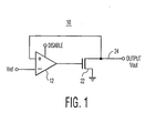
- FIG. 1 shows a voltage stabilized low level driver 10.
- Driver 10 comprises an operational amplifier (op-amp) 12 and a switching circuit, e.g., an output NMOS transistor 22 having an open-drain output V out .
- Op-amp 12 has its positive input terminal connected to an output node 24, forming a feedback loop and its negative input terminal connected to a reference voltage, Vref.
- Op-amp 12 also has its output connected to the gate of transistor 22.
- op-amp 12 drives transistor 22 such that the feedback mechanism causes the output voltage Vout to match the reference voltage, Vref.
- the op-amp 12 is disabled by a disable signal, the op-amp turns off transistor 22 to allow output node 24 to have a high impedance. Therefore, the output voltage Vout can be pulled up to approximately the digital supply voltage level V cc by an external resistor or current source (not shown).
- FIG. 2 shows a voltage stabilized low level driver 30 according to the invention.
- Driver 30 is a variation of driver 10 in FIG. 1 .
- driver 30 includes an output protection circuit 32, input protection circuits 34 and 36, and a slew rate control circuit 38.
- Output protection circuit 32 is placed in series with transistor 22.
- Two input protection circuits 34 and 36 are placed in series with the two input terminals of op-amp 12, respectively, to maintain symmetry and noise rejection.
- slew rate control circuit 38 is connected between output node 24 and the gate of transistor 22.
- op-amp 12 when op-amp 12 is enabled, it acts as a feedback mechanism driving the gate of transistor 22 high to turn the transistor on. Slew rate control circuit 38 limits how quickly transistor 22 can be turned on. As the voltage Vout at output node 24 falls to the reference voltage V ref , op-amp 12 reduces the gate voltage of transistor 22 to the point that transistor 22 sinks just enough current from output node 24 to make the output voltage Vout match the reference voltage V ref .
- an industry standard type band-gap reference is used to generate the reference voltage, Vref.
- V ref is 0.52 V.
- the band-gap is also used to generate a reference current I in (shown in FIG. 3 ) to set the tail current in the op-amp.
- Other types of reference voltage and current may also be used with little or no effect on the circuit behavior.
- the voltage stabilized low level driver provides 100 mV stability of output low level independent of temperature, Vcc, load current and load capacitance.
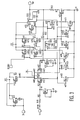
- FIG. 3 shows the schematics of driver 30 in FIG. 2 .
- an input reference current I in is reflected using a current mirror comprised of transistors M138 and M139 to provide the tail current for the input pair of transistors M140 and M141.
- Resistor R150 and NMOS transistor M154 comprise the secondary input gate protection in addition to primary ESD (electrostatic discharge) protection circuit (not shown).
- R150 and M154 are matched with resistor R149 and transistor M153 for noise immunity considerations.
- the output currents from the input pair M140, M141 flow through diode wired transistors M158 and M159 and are mirrored onto transistors M160 and M161, respectively.
- the current through M160 is reflected through a current mirror comprised of transistors M142 and M143 to become the pull-up current which is summed against the pull-down current of M161 for the gate drive of transistor M157, which is the output NMOS transistor.
- the op-amp frequency compensation is provided by capacitor I146 and resistor R148.
- Transistors M144, M145, M162, and M156 are used to disable the pull-up current_mirror M142 and M143 and to pull the gate of the output NMOS transistor M157 down when the output NMOS transistor M157 is switched off.
- Diode wired transistors M182 and M155 along with capacitor I147 and resistor R151 comprise the slew rate control circuit which limits the slew rate of the output high-to-low transition as transistor M157 turns on.
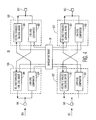
- FIG. 4 shows a repeater 50 according to the present invention. It illustrates the use of the voltage stabilized low level driver of the present invention in an I 2 C bus interface application.
- An I 2 C bus is an industry standard bus interface developed by Philips Corporation which allows integrated circuits to communicated directly with each other via a simple bi-directional 2-wire bus.
- Interfacing devices in a I 2 C based system can be achieved by directly connecting them to the two bus lines: a serial data line (SDA) and a serial clock line (SCL).
- SDA serial data line
- SCL serial clock line
- repeater 50 comprises four identical I/O cells, 52A, 52B, 52C, and 52D.
- Cells 52A and 52B are connected to each other on the SDA line between I/O pads 54A and 54B.
- cells 52C and 52D are connected on the SCL line between I/O pads 54C and 54D.
- Each cell includes a voltage stabilized low level driver and a low level comparator.
- cell 52A includes a voltage stabilized low level driver 58A and a low level comparator 60A.
- a bandgap reference block 56 is connected to the blocks in each I/O cell. Bandgap reference block 56 generates bandgap reference derived voltages Vref and V R , as well as a reference current (not shown) for the op-amps in drivers 58A, 58B, 58C and 58D.
- low level comparator 60A compares it with a bandgap reference derived voltage, V R (e.g., 0.45 V). After determining that L 1 is less than V R , comparator 60A outputs a low signal L 1 to voltage stabilized low level driver 58B.
- the low signal L 1 from comparator 60A causes driver 58B to turn on by enabling the op-amp in driver 58B, which in turn pulls pad 54B to a low level L 2 to match Vref (e.g., 0.52 V).
- Vref which is also a bandgap reference derived voltage
- L 1 received at pad 54A is higher than L 1 received at pad 54A and is thus treated as a high signal by comparator 60B.
- comparator 60B outputs an internal high signal H int (approximately equal to a digital supply voltage V cc ) to driver 58A.
- High signal H int causes driver 58A to remain off.
- the output of driver 58A is off. Therefore, the voltage at pad 54A remains at L 1 . This allows latch-up free I/O pads to be achieved.
- comparator 60A sends a high signal H int to driver 58B after comparing H ext with V R .
- the high signal H int causes driver 58B to turn off. Therefore, the output of driver 58B and pad 54B are pulled up to H ext by an external pull-up resistor or current source (assuming the pad is not otherwise pulled down by other circuits).
- Comparator 60B compares H ext at pad 54B with V R and outputs an internal high signal H int to driver 58A. The internal high signal H int causes driver 58A to stay off.
- the output of driver 58A remains off. Therefore, the voltage at pad 54A remains at H ext caused by the external pull-up resistor or current source. This allows latch-up free I/O pads to be achieved.
- cells 52C and 52D on the SCL line are similar to the operations of 52A and 52B on the SDA line described above and the description is therefore omitted.
- additional capacitive loads are allowed to be added to the I 2 C bus interface (which has a limitation on the total allowed capacitive loads). This is achieved by splitting the capacitive loads on the SDA and SCL lines so that the total capacitive loads may be doubled.
Landscapes
- Physics & Mathematics (AREA)
- Engineering & Computer Science (AREA)
- Computer Hardware Design (AREA)
- Computing Systems (AREA)
- General Engineering & Computer Science (AREA)
- Mathematical Physics (AREA)
- Logic Circuits (AREA)
- Electronic Switches (AREA)
- Continuous-Control Power Sources That Use Transistors (AREA)
- Dc Digital Transmission (AREA)
- Amplifiers (AREA)
Claims (10)
- Spannungstreiber, der einen Ausgangsknoten aufweist, umfassend:eine Umschaltschaltung (22), die einen Steueranschluss und einen mit dem Ausgangsknoten gekoppelten Ausgangsanschluss aufweist;einen Operationsverstärker (12) der einen mit dem Ausgangsknoten verbundenen ersten Eingangsanschluss, einen mit einer Eingangsreferenzspannung verbundenen zweiten Eingangsanschluss, und einen mit dem Steueranschluss der Umschaltschaltung verbundenen Ausgangsanschluss aufweist, wobei der Verstärker durch ein externes Sperrsignal zum Einschalten und Ausschalten des Verstärkers gesteuert wird;eine Flankensteilheitsteuerschaltung (38), die zwischen dem Ausgangsknoten und dem Steueranschluss der Umschaltschaltung angeschlossen ist; wobeider Verstärker beim Einschalten den Steueranschluss der Umschaltschaltung so ansteuert, dass der Ausgangsknoten veranlasst wird, sich an die Referenzspannung anzupassen; und wobei der Verstärker beim Ausschalten den Steueranschluss der Umschaltschaltung so ansteuert, dass der Ausgangsknoten veranlasst wird, eine hohe Impedanz aufzuweisen.
- Treiber nach Anspruch 1, wobei die Umschaltschaltung ein Transistor ist und der Steueranschluss ein Gate-Anschluss des Transistors ist.
- Treiber nach Anspruch 1, wobei die hohe Impedanz des Ausgangsknotens erlaubt, dass der Ausgangknoten durch eine externe Vorrichtung auf einen vorgegebenen Pegel gezogen wird.
- Treiber nach Anspruch 1, ferner umfassend:eine Ausgangsschutzschaltung (32), die zwischen dem Ausgangsknoten und dem Ausgangsanschluss der Umschaltschaltung angeschlossen ist;eine erste Eingangsschutzschaltung (36), die zwischen dem ersten Eingangsanschluss des Verstärkers und dem Ausgangsknoten angeschlossen ist; undeine zweite Eingangsschutzschaltung (34), die zwischen dem zweiten Eingangsanschluss des Verstärkers und einer Eingangsreferenzspannung angeschlossen ist.
- Treiber nach Anspruch 4, wobei die erste und die zweite Eingangsschutzschaltung Symmetrie und Rauschunterdrückung aufrechterhalten.
- Zwischenverstärker (50), der erste und zweite Enden aufweist und einen Treiber nach irgendeinem der vorangehenden Ansprüche umfasst.
- Zwischenverstärker nach Anspruch 6, ferner umfassend:eine erste E/A-Zelle (52A), enthaltend:einen ersten Spannungstreiber (58A) mit einem ersten Eingangsanschluss, einem zweiten Eingangsanschluss, der mit einer ersten Referenzspannung verbunden ist, und einem Ausgangsanschluss, der mit dem ersten Ende gekoppelt ist, undeinen ersten Komparator (60A), dessen erster Eingangsanschluss mit dem ersten Ende gekoppelt ist, und dessen zweiter Eingangsanschluss mit der zweiten Referenzspannung gekoppelt ist, die kleiner ist als die erste Referenzspannung, wobei der erste Komparator ein Eingangssignal über das erste Ende empfängt und ein erstes Ergebnissignal an seinem Ausgangsanschluss auf der Grundlage eines Vergleichs des Eingangssignals mit der zweiten Referenzspannung ausgibt; undeine zweite E/A-Zelle (52B), enthaltend:einen ersten Spannungstreiber (58B), dessen erster Eingangsanschluss mit dem Ausgangsanschluss des ersten Komparators gekoppelt ist, dessen zweiter Eingangsanschluss mit der ersten Referenzspannung gekoppelt ist, und dessen Ausgangsanschluss mit dem zweiten Ende gekoppelt ist, wobei der zweite Spannungstreiber das erste Ergebnissignal empfängt und ein zweites Ansteuersignal über seinen Ausgangsanschluss an das zweite Ende ausgibt, undeinen zweiten Komparator (60B), dessen erster Eingangsanschluss mit dem zweiten Ende gekoppelt ist, dessen zweiter Eingangsanschluss mit der zweiten Referenzspannung gekoppelt ist, und dessen Ausgangsanschluss mit dem ersten Eingangsanschluss des ersten Spannungstreibers gekoppelt ist, wobei der zweite Komparator das erste Ansteuersignal empfängt und ein zweites Ergebnissignal über seinen Ausgangsanschluss an den ersten Spannungstreiber auf der Grundlage eines Vergleichs des ersten Ansteuersignals und der zweiten Referenzspannung ausgibt;wobei der erste Spannungstreiber das zweite Ergebnissignal empfängt und ein erstes Ansteuersignal über seinen Ausgangsanschluss an das erste Ende ausgibt.
- Zwischenverstärker nach Anspruch 7, ferner umfassend:eine dritte E/A-Zelle (52C), die mit der ersten E/A-Zelle identisch ist; undeine vierte E/A-Zelle (52D), die mit der zweiten E/A-Zelle identisch ist und mit der dritten E/A-Zelle in derselben Weise verbunden ist wie die ersten und zweiten E/A-Zellen verbunden sind.
- Zwischenverstärker nach Anspruch 7, wobei die erste und die zweite E/A-Zelle auf einer SDA-Leitung einer 12C-Bus-Schnittstelle verwenden werden.
- Zwischenverstärker nach Anspruch 8, wobei die dritte und die vierte E/A-Zelle auf einer SCL-Leitung einer 12C-Bus-Schnittstelle verwendet werden.
Applications Claiming Priority (3)
| Application Number | Priority Date | Filing Date | Title |
|---|---|---|---|
| US642181 | 1984-08-17 | ||
| US09/642,181 US6433622B1 (en) | 2000-08-17 | 2000-08-17 | Voltage stabilized low level driver |
| PCT/EP2001/009340 WO2002015401A2 (en) | 2000-08-17 | 2001-08-10 | Voltage stabilized low level driver |
Publications (2)
| Publication Number | Publication Date |
|---|---|
| EP1312166A2 EP1312166A2 (de) | 2003-05-21 |
| EP1312166B1 true EP1312166B1 (de) | 2009-04-15 |
Family
ID=24575533
Family Applications (1)
| Application Number | Title | Priority Date | Filing Date |
|---|---|---|---|
| EP01958069A Expired - Lifetime EP1312166B1 (de) | 2000-08-17 | 2001-08-10 | Spannungsstabilisierter niedrigpegeltreiber |
Country Status (8)
| Country | Link |
|---|---|
| US (1) | US6433622B1 (de) |
| EP (1) | EP1312166B1 (de) |
| JP (1) | JP2004507143A (de) |
| KR (1) | KR100849510B1 (de) |
| AT (1) | ATE429074T1 (de) |
| DE (1) | DE60138392D1 (de) |
| TW (1) | TW518822B (de) |
| WO (1) | WO2002015401A2 (de) |
Families Citing this family (5)
| Publication number | Priority date | Publication date | Assignee | Title |
|---|---|---|---|---|
| US7372291B2 (en) * | 2005-09-30 | 2008-05-13 | Stmicroelectronics Asia Pacific Pte. Ltd. | Circuits having precision voltage clamping levels and method |
| US8008953B1 (en) * | 2008-11-07 | 2011-08-30 | Silego Technology, Inc. | Gate control circuit |
| US9225293B2 (en) * | 2011-07-10 | 2015-12-29 | Triune Systems, LLC | Pop and click noise reduction |
| US10574297B2 (en) | 2009-11-25 | 2020-02-25 | Triune Ip, Llc | Multi-use wireless power and data system |
| US7999569B2 (en) * | 2009-12-03 | 2011-08-16 | Nxp B.V. | Edge rate suppression for open drain buses |
Family Cites Families (5)
| Publication number | Priority date | Publication date | Assignee | Title |
|---|---|---|---|---|
| US4992677A (en) | 1988-03-23 | 1991-02-12 | Hitachi, Ltd. | High speed MOSFET output buffer with low noise |
| CA2066929C (en) * | 1991-08-09 | 1996-10-01 | Katsuji Kimura | Temperature sensor circuit and constant-current circuit |
| JP3085562B2 (ja) * | 1992-10-12 | 2000-09-11 | 三菱電機株式会社 | 基準電圧発生回路および内部降圧回路 |
| JP3494488B2 (ja) * | 1994-11-25 | 2004-02-09 | 株式会社ルネサステクノロジ | 半導体装置 |
| KR100294450B1 (ko) * | 1998-09-24 | 2001-09-17 | 윤종용 | 반도체메모리장치의어레이내부전원전압발생회로 |
-
2000
- 2000-08-17 US US09/642,181 patent/US6433622B1/en not_active Expired - Lifetime
-
2001
- 2001-08-10 DE DE60138392T patent/DE60138392D1/de not_active Expired - Lifetime
- 2001-08-10 AT AT01958069T patent/ATE429074T1/de not_active IP Right Cessation
- 2001-08-10 KR KR1020027004854A patent/KR100849510B1/ko not_active Expired - Fee Related
- 2001-08-10 WO PCT/EP2001/009340 patent/WO2002015401A2/en not_active Ceased
- 2001-08-10 EP EP01958069A patent/EP1312166B1/de not_active Expired - Lifetime
- 2001-08-10 JP JP2002520413A patent/JP2004507143A/ja not_active Withdrawn
- 2001-10-16 TW TW090125536A patent/TW518822B/zh not_active IP Right Cessation
Also Published As
| Publication number | Publication date |
|---|---|
| TW518822B (en) | 2003-01-21 |
| US6433622B1 (en) | 2002-08-13 |
| KR100849510B1 (ko) | 2008-07-31 |
| DE60138392D1 (de) | 2009-05-28 |
| EP1312166A2 (de) | 2003-05-21 |
| KR20020064883A (ko) | 2002-08-10 |
| JP2004507143A (ja) | 2004-03-04 |
| WO2002015401A3 (en) | 2002-08-08 |
| WO2002015401A2 (en) | 2002-02-21 |
| ATE429074T1 (de) | 2009-05-15 |
Similar Documents
| Publication | Publication Date | Title |
|---|---|---|
| US5206544A (en) | CMOS off-chip driver with reduced signal swing and reduced power supply disturbance | |
| US6236239B1 (en) | Output buffer circuit achieving stable operation and cost reduction | |
| US5867015A (en) | Low drop-out voltage regulator with PMOS pass element | |
| EP0397268B1 (de) | Integrierte Schaltung mit einem Signalpegelumsetzer | |
| US5367210A (en) | Output buffer with reduced noise | |
| EP0143699A2 (de) | Bus-Sender/Empfänger | |
| TW521494B (en) | Process compensated integrated circuitry | |
| US6600361B2 (en) | Semiconductor device | |
| JP3335183B2 (ja) | バッファ回路 | |
| US5929679A (en) | Voltage monitoring circuit capable of reducing power dissipation | |
| US6639390B2 (en) | Protection circuit for miller compensated voltage regulators | |
| JP3613528B2 (ja) | 制御型スルーレート出力バッファ | |
| EP1312166B1 (de) | Spannungsstabilisierter niedrigpegeltreiber | |
| JP4939895B2 (ja) | レベルシフタ回路 | |
| US5124595A (en) | Gate drive bias circuit for MOSFET power switches | |
| US6236195B1 (en) | Voltage variation correction circuit | |
| US6281744B1 (en) | Voltage drop circuit | |
| US6400177B1 (en) | Output driver and method for meeting specified output impedance and current characteristics | |
| KR100714668B1 (ko) | 부하 커패시턴스 보상 버퍼, 장치 및 그 방법 | |
| JP2001127805A (ja) | 終端回路 | |
| US7113007B2 (en) | Driver circuit and system including driver circuit | |
| US5532617A (en) | CMOS input with temperature and VCC compensated threshold | |
| US7852120B2 (en) | Bi-directional buffer for open-drain or open-collector bus | |
| US11211905B2 (en) | Semiconductor device and memory system | |
| US5999017A (en) | CMOS implemented output buffer circuit for providing ECL level signals |
Legal Events
| Date | Code | Title | Description |
|---|---|---|---|
| PUAI | Public reference made under article 153(3) epc to a published international application that has entered the european phase |
Free format text: ORIGINAL CODE: 0009012 |
|
| 17P | Request for examination filed |
Effective date: 20030317 |
|
| AK | Designated contracting states |
Designated state(s): AT BE CH CY DE DK ES FI FR GB GR IE IT LI LU MC NL PT SE TR |
|
| RAP1 | Party data changed (applicant data changed or rights of an application transferred) |
Owner name: NXP B.V. |
|
| 17Q | First examination report despatched |
Effective date: 20080312 |
|
| GRAP | Despatch of communication of intention to grant a patent |
Free format text: ORIGINAL CODE: EPIDOSNIGR1 |
|
| GRAS | Grant fee paid |
Free format text: ORIGINAL CODE: EPIDOSNIGR3 |
|
| GRAA | (expected) grant |
Free format text: ORIGINAL CODE: 0009210 |
|
| AK | Designated contracting states |
Kind code of ref document: B1 Designated state(s): AT BE CH CY DE DK ES FI FR GB GR IE IT LI LU MC NL PT SE TR |
|
| REG | Reference to a national code |
Ref country code: GB Ref legal event code: FG4D Ref country code: CH Ref legal event code: EP |
|
| REG | Reference to a national code |
Ref country code: IE Ref legal event code: FG4D |
|
| REF | Corresponds to: |
Ref document number: 60138392 Country of ref document: DE Date of ref document: 20090528 Kind code of ref document: P |
|
| NLV1 | Nl: lapsed or annulled due to failure to fulfill the requirements of art. 29p and 29m of the patents act | ||
| PG25 | Lapsed in a contracting state [announced via postgrant information from national office to epo] |
Ref country code: AT Free format text: LAPSE BECAUSE OF FAILURE TO SUBMIT A TRANSLATION OF THE DESCRIPTION OR TO PAY THE FEE WITHIN THE PRESCRIBED TIME-LIMIT Effective date: 20090415 Ref country code: ES Free format text: LAPSE BECAUSE OF FAILURE TO SUBMIT A TRANSLATION OF THE DESCRIPTION OR TO PAY THE FEE WITHIN THE PRESCRIBED TIME-LIMIT Effective date: 20090726 Ref country code: PT Free format text: LAPSE BECAUSE OF FAILURE TO SUBMIT A TRANSLATION OF THE DESCRIPTION OR TO PAY THE FEE WITHIN THE PRESCRIBED TIME-LIMIT Effective date: 20090915 Ref country code: FI Free format text: LAPSE BECAUSE OF FAILURE TO SUBMIT A TRANSLATION OF THE DESCRIPTION OR TO PAY THE FEE WITHIN THE PRESCRIBED TIME-LIMIT Effective date: 20090415 |
|
| PG25 | Lapsed in a contracting state [announced via postgrant information from national office to epo] |
Ref country code: NL Free format text: LAPSE BECAUSE OF FAILURE TO SUBMIT A TRANSLATION OF THE DESCRIPTION OR TO PAY THE FEE WITHIN THE PRESCRIBED TIME-LIMIT Effective date: 20090415 Ref country code: SE Free format text: LAPSE BECAUSE OF FAILURE TO SUBMIT A TRANSLATION OF THE DESCRIPTION OR TO PAY THE FEE WITHIN THE PRESCRIBED TIME-LIMIT Effective date: 20090715 |
|
| PG25 | Lapsed in a contracting state [announced via postgrant information from national office to epo] |
Ref country code: DK Free format text: LAPSE BECAUSE OF FAILURE TO SUBMIT A TRANSLATION OF THE DESCRIPTION OR TO PAY THE FEE WITHIN THE PRESCRIBED TIME-LIMIT Effective date: 20090415 |
|
| PLBE | No opposition filed within time limit |
Free format text: ORIGINAL CODE: 0009261 |
|
| STAA | Information on the status of an ep patent application or granted ep patent |
Free format text: STATUS: NO OPPOSITION FILED WITHIN TIME LIMIT |
|
| PG25 | Lapsed in a contracting state [announced via postgrant information from national office to epo] |
Ref country code: BE Free format text: LAPSE BECAUSE OF FAILURE TO SUBMIT A TRANSLATION OF THE DESCRIPTION OR TO PAY THE FEE WITHIN THE PRESCRIBED TIME-LIMIT Effective date: 20090415 |
|
| 26N | No opposition filed |
Effective date: 20100118 |
|
| PG25 | Lapsed in a contracting state [announced via postgrant information from national office to epo] |
Ref country code: MC Free format text: LAPSE BECAUSE OF NON-PAYMENT OF DUE FEES Effective date: 20090831 |
|
| REG | Reference to a national code |
Ref country code: CH Ref legal event code: PL |
|
| PG25 | Lapsed in a contracting state [announced via postgrant information from national office to epo] |
Ref country code: CH Free format text: LAPSE BECAUSE OF NON-PAYMENT OF DUE FEES Effective date: 20090831 Ref country code: LI Free format text: LAPSE BECAUSE OF NON-PAYMENT OF DUE FEES Effective date: 20090831 |
|
| PG25 | Lapsed in a contracting state [announced via postgrant information from national office to epo] |
Ref country code: IE Free format text: LAPSE BECAUSE OF NON-PAYMENT OF DUE FEES Effective date: 20090810 |
|
| PG25 | Lapsed in a contracting state [announced via postgrant information from national office to epo] |
Ref country code: GR Free format text: LAPSE BECAUSE OF FAILURE TO SUBMIT A TRANSLATION OF THE DESCRIPTION OR TO PAY THE FEE WITHIN THE PRESCRIBED TIME-LIMIT Effective date: 20090716 |
|
| PG25 | Lapsed in a contracting state [announced via postgrant information from national office to epo] |
Ref country code: IT Free format text: LAPSE BECAUSE OF FAILURE TO SUBMIT A TRANSLATION OF THE DESCRIPTION OR TO PAY THE FEE WITHIN THE PRESCRIBED TIME-LIMIT Effective date: 20090415 |
|
| PG25 | Lapsed in a contracting state [announced via postgrant information from national office to epo] |
Ref country code: LU Free format text: LAPSE BECAUSE OF NON-PAYMENT OF DUE FEES Effective date: 20090810 |
|
| PG25 | Lapsed in a contracting state [announced via postgrant information from national office to epo] |
Ref country code: TR Free format text: LAPSE BECAUSE OF FAILURE TO SUBMIT A TRANSLATION OF THE DESCRIPTION OR TO PAY THE FEE WITHIN THE PRESCRIBED TIME-LIMIT Effective date: 20090415 |
|
| PG25 | Lapsed in a contracting state [announced via postgrant information from national office to epo] |
Ref country code: CY Free format text: LAPSE BECAUSE OF FAILURE TO SUBMIT A TRANSLATION OF THE DESCRIPTION OR TO PAY THE FEE WITHIN THE PRESCRIBED TIME-LIMIT Effective date: 20090415 |
|
| PGFP | Annual fee paid to national office [announced via postgrant information from national office to epo] |
Ref country code: GB Payment date: 20120725 Year of fee payment: 12 |
|
| REG | Reference to a national code |
Ref country code: GB Ref legal event code: 732E Free format text: REGISTERED BETWEEN 20130606 AND 20130612 |
|
| GBPC | Gb: european patent ceased through non-payment of renewal fee |
Effective date: 20130810 |
|
| PG25 | Lapsed in a contracting state [announced via postgrant information from national office to epo] |
Ref country code: GB Free format text: LAPSE BECAUSE OF NON-PAYMENT OF DUE FEES Effective date: 20130810 |
|
| REG | Reference to a national code |
Ref country code: DE Ref legal event code: R084 Ref document number: 60138392 Country of ref document: DE |
|
| REG | Reference to a national code |
Ref country code: DE Ref legal event code: R084 Ref document number: 60138392 Country of ref document: DE Effective date: 20141015 |
|
| REG | Reference to a national code |
Ref country code: FR Ref legal event code: PLFP Year of fee payment: 15 |
|
| REG | Reference to a national code |
Ref country code: FR Ref legal event code: PLFP Year of fee payment: 16 |
|
| REG | Reference to a national code |
Ref country code: DE Ref legal event code: R082 Ref document number: 60138392 Country of ref document: DE Representative=s name: EISENFUEHR SPEISER PATENTANWAELTE RECHTSANWAEL, DE Ref country code: DE Ref legal event code: R081 Ref document number: 60138392 Country of ref document: DE Owner name: NEXPERIA B.V., NL Free format text: FORMER OWNER: NXP B.V., EINDHOVEN, NL Ref country code: DE Ref legal event code: R081 Ref document number: 60138392 Country of ref document: DE Owner name: NXP B.V., NL Free format text: FORMER OWNER: NXP B.V., EINDHOVEN, NL |
|
| REG | Reference to a national code |
Ref country code: FR Ref legal event code: TP Owner name: NEXPERIA B.V., NL Effective date: 20161109 |
|
| REG | Reference to a national code |
Ref country code: FR Ref legal event code: TP Owner name: NXP B.V., NL Effective date: 20170113 |
|
| REG | Reference to a national code |
Ref country code: DE Ref legal event code: R082 Ref document number: 60138392 Country of ref document: DE Ref country code: DE Ref legal event code: R081 Ref document number: 60138392 Country of ref document: DE Owner name: NXP B.V., NL Free format text: FORMER OWNER: NEXPERIA B.V., EINDHOVEN, NL |
|
| REG | Reference to a national code |
Ref country code: FR Ref legal event code: PLFP Year of fee payment: 17 |
|
| REG | Reference to a national code |
Ref country code: FR Ref legal event code: PLFP Year of fee payment: 18 |
|
| PGFP | Annual fee paid to national office [announced via postgrant information from national office to epo] |
Ref country code: FR Payment date: 20190722 Year of fee payment: 19 Ref country code: DE Payment date: 20190722 Year of fee payment: 19 |
|
| REG | Reference to a national code |
Ref country code: DE Ref legal event code: R119 Ref document number: 60138392 Country of ref document: DE |
|
| PG25 | Lapsed in a contracting state [announced via postgrant information from national office to epo] |
Ref country code: DE Free format text: LAPSE BECAUSE OF NON-PAYMENT OF DUE FEES Effective date: 20210302 Ref country code: FR Free format text: LAPSE BECAUSE OF NON-PAYMENT OF DUE FEES Effective date: 20200831 |