US5124595A - Gate drive bias circuit for MOSFET power switches - Google Patents

Gate drive bias circuit for MOSFET power switches Download PDF

Info

Publication number
US5124595A
US5124595A US07/712,571 US71257191A US5124595A US 5124595 A US5124595 A US 5124595A US 71257191 A US71257191 A US 71257191A US 5124595 A US5124595 A US 5124595A
Authority
US
United States
Prior art keywords
turn
snubber
capacitor
bias
gate
Prior art date
Legal status (The legal status is an assumption and is not a legal conclusion. Google has not performed a legal analysis and makes no representation as to the accuracy of the status listed.)
Expired - Fee Related
Application number
US07/712,571
Inventor
Josh Mandelcorn
Current Assignee (The listed assignees may be inaccurate. Google has not performed a legal analysis and makes no representation or warranty as to the accuracy of the list.)
Pioneer Magnetics Inc
Original Assignee
Pioneer Magnetics Inc
Priority date (The priority date is an assumption and is not a legal conclusion. Google has not performed a legal analysis and makes no representation as to the accuracy of the date listed.)
Filing date
Publication date
Application filed by Pioneer Magnetics Inc filed Critical Pioneer Magnetics Inc
Priority to US07/712,571 priority Critical patent/US5124595A/en
Assigned to PIONEER MAGNETICS, INC., reassignment PIONEER MAGNETICS, INC., ASSIGNMENT OF ASSIGNORS INTEREST. Assignors: NABDEKCIRBM HISH
Application granted granted Critical
Publication of US5124595A publication Critical patent/US5124595A/en
Anticipated expiration legal-status Critical
Expired - Fee Related legal-status Critical Current

Links

Images

Classifications

    • HELECTRICITY
    • H03ELECTRONIC CIRCUITRY
    • H03KPULSE TECHNIQUE
    • H03K17/00Electronic switching or gating, i.e. not by contact-making and –breaking
    • H03K17/04Modifications for accelerating switching
    • H03K17/041Modifications for accelerating switching without feedback from the output circuit to the control circuit
    • H03K17/0412Modifications for accelerating switching without feedback from the output circuit to the control circuit by measures taken in the control circuit
    • H03K17/04123Modifications for accelerating switching without feedback from the output circuit to the control circuit by measures taken in the control circuit in field-effect transistor switches
    • HELECTRICITY
    • H03ELECTRONIC CIRCUITRY
    • H03KPULSE TECHNIQUE
    • H03K17/00Electronic switching or gating, i.e. not by contact-making and –breaking
    • H03K17/06Modifications for ensuring a fully conducting state
    • H03K17/063Modifications for ensuring a fully conducting state in field-effect transistor switches
    • HELECTRICITY
    • H03ELECTRONIC CIRCUITRY
    • H03KPULSE TECHNIQUE
    • H03K17/00Electronic switching or gating, i.e. not by contact-making and –breaking
    • H03K17/08Modifications for protecting switching circuit against overcurrent or overvoltage
    • H03K17/081Modifications for protecting switching circuit against overcurrent or overvoltage without feedback from the output circuit to the control circuit
    • H03K17/0814Modifications for protecting switching circuit against overcurrent or overvoltage without feedback from the output circuit to the control circuit by measures taken in the output circuit
    • H03K17/08142Modifications for protecting switching circuit against overcurrent or overvoltage without feedback from the output circuit to the control circuit by measures taken in the output circuit in field-effect transistor switches

Definitions

  • MOSFETS power field effect transistors
  • Extra auxiliary transformer windings are usually required in such prior art power supplies to assure proper operation of the MOSFET power switches.
  • this adds substantial complexity to the auxiliary supply system, especially if negative bias for speeding up the turn-off speed of the MOSFETS is required, and when more than one group of MOSFETS with different source potentials are used.
  • a more recent prior art power supply system uses snubber circuitry in conjunction with the MOSFET power switches to charge the positive gate bias for the MOSFET power switches during each cycle when the MOSFETS are turned off.
  • snubbers are normally used to reduce turn-off stresses of controlled semi-conductor switches.
  • the snubber usually includes a capacitor in parallel with the semi-conductor switch to reduce the rate of rise of voltage across the switch when the switch is turned off, absorbing energy that would have had to be dissipated by the switch.
  • Conventional snubber circuitry introduces losses since the charge on the capacitor is dissipated through a resistor to prepare for the next switch turn-off.
  • the semi-conductor switch carries the discharge current of the capacitor when the switch is on.
  • an objective of the present invention is to provide an improved and simple circuit for producing gate drive bias for the MOSFET power switches which forces the MOSFETS to share the turn-off voltage when they are connected in series.
  • Another objective of the invention is to provide such an improved circuit which generates a negative gate bias for the MOSFETS in order to speed up switch-off of the MOSFETS.
  • FIG. 1 is a circuit diagram of a prior art switching circuit which includes a pair of MOSFET power switches, and which uses snubber circuitry to control the gate bias of the MOSFETS;
  • FIG. 2 is a series of wave forms of signals occurring throughout the circuit of FIG. 1;
  • FIG. 3 is circuit diagram of a switching circuit like FIG. 1, but which includes certain modifications in order to achieve the objectives of the invention
  • FIG. 4 is a series of curves illustrating signals occurring throughout the circuit of FIG. 3;
  • FIG. 5 is a circuit diagram of a gate drive module included in the circuits of FIGS. 1 and 3.
  • the circuit of FIG. 1 includes a gate drive module represented by a block 10.
  • This module operates in a manner to respond to pulse-width modulated drive pulses (FIG. 2A) from a pulse-width modulator 12 to drive a pair of MOSFETS Q1, Q2.
  • the output of the drive module (FIG. 2B) is introduced to the gate electrodes of the MOSFETS Q1, Q2 through respective 10 Ohm resistors R1 and R2.
  • the circuit of FIG. 1 includes a positive bias supply Zener Diode CR1, which may be of the type designated IN4744.
  • Zener Diode CR1 is shunted by a 1 microfarad by-pass capacitor C2.
  • the Zener diode is connected to through a 100 kilo-ohm resistor R3 to a positive potential lead 100 which is connected to the drain electrodes of MOSFETS Q1, Q2.
  • the Zener diode is also connected to a common grounded lead 102 which, in turn, is connected to the drive module 10.
  • the source electrodes of MOSFETS Q1 and Q2 are also connected to common grounded lead 102.
  • capacitor C2 are charged, for example, to 10-15 volts through resistor R3. This is achieved before the MOSFETS Q1, Q2 turn-on because, when the MOSFETS are turned off there is substantial voltage V DS between the leads 100 and 102 (FIG. 2C), and the drive module 10 draws negligible current in the steady turned-off state of the circuit.
  • the circuit of FIG. 1 also includes a 0.0027 microfarad snubber capacitor C1 connected to lead 100 and to a steering diode CR2.
  • the diode may be of the type designated MUR160.
  • Diode CR2 is connected to a 1 microfarad capacitor C2 which, in turn, is connected to lead 102.
  • the junction of diode CR2 and capacitor C2 is connected to the junction of resistor R3 and Zener diode CR1 and to the gate drive module 10. In this manner, positive bias (FIG. 2D) is supplied to the drive module.
  • the circuit of FIG. 1 also includes a 100 ohm main snubber resistor R4 which is connected to the junction of capacitor C1 and diode CR2, and which is also connected to lead 102 through a diode CR3.
  • the diode may be of the type designated 1N4937.
  • the cathode of the diode CR3 is connected to the gate drive module 10 to provide a sense point for the drive module.
  • the positive bias supply capacitor C2 is charged when the MOSFETS Q1, Q2 are turned off. At that time, a current IC 1 flows through the snubber capacitor C1 and through the steering diode CR2 into capacitor C2. The direction of the current flow IC 1 is shown by the arrow in FIG. 1.
  • Capacitor C1 charges up to substantially the drain-source voltage (V DS ) of the turned-off power switches Q1, Q2 (FIG. 2--curve C). Accordingly, the total charge available to the positive bias supply (CR2, CR1) is C1 ⁇ V DS (off). The average available positive bias current is the aforesaid charge multiplied by the switching frequency or C1 V DS ⁇ F) (FIG. 2--curve D).
  • the snubber capacitor C1 discharges through the main snubber resistor R4 and steering diode CR3 (FIG. 2E).
  • the drive module uses the sense point from the cathode of diode CR3 to hold the gate drive module turned-off when the MOSFETS Q1, Q2 are supposed to be off, even when positive excursions occur on the drain electrodes of the MOSFETS.
  • the circuit of FIG. 1 is modified in accordance with the teaching of the present invention by inserting a 1 microfarad capacitor C3, shunted by a Zener diode CR4, in series between the anode of diode CR3 and lead 102; by connecting the anode of the diode CR3 to the gate drive module 10 to supply a negative bias to the gate drive module; and by introducing a 75 ohm resistor R5 between resistor R3 and the cathode of Zener diode CR1.
  • Zener diode CR4 may be of the type designated IN751C.
  • the current flowing through the snubber resistor R4 and through diode CR3 during the turn-on of the MOSFETS power switches Q1, Q2 is caused to flow through capacitor C3 and through Zener diode CR4.
  • This current flow generates a negative DC bias of, for example, 5.1 volts in the gate drive module 10.
  • the steering diode CR3 prevents this negative bias from being drained away when the voltage on capacitor C1 and resistor R4 goes positive.
  • This negative bias approximately doubles the turn-off speed of the MOSFETS power switches Q1 and Q2, which greatly reduces the size of the snubber circuit required for the power switches, and/or reduces the turn-off losses of the power switches.
  • the gate module Since the available charge per cycle from the snubber capacitor C1 is the same in the charging mode (turn-off) and discharging mode (turn-on), and the gate module derives the same current from both the positive bias and negative bias; if the drive bias for the positive bias is adequate, it will be sufficient for the negative bias. The only difference is that for a larger gate voltage excursion due to the negative bias, the total QG (Gate charge) is slightly larger. This affects both the positive bias and the negative bias demand equally.
  • the balancing scheme forces a turn-off delay into the MOSFET group that tends to draw the turn-off voltage, thereby forcing the MOSFETS groups to share the turn-off voltage. If one group of MOSFETS tends to draw the turn-off voltage, more current will become available to the positive bias supply of that groups' gate drive since available current is proportional to V DS (V DS C1 ⁇ F). Since the gate drive demand remains relatively constant, this excessive gate bias supply current will flow through resistor R5 thereby increasing the positive bias voltage. This positive bias voltage will allow the gate electrodes to charge to the higher positive voltage.
  • FIGS. 4A-4E are the same as those in FIGS. 2A-2E, with the exception that the gate voltage of curve B is shifted to extend, for example, between -4 and +13 volts, instead of 0 and +15 volts as in the circuit of FIG. 1.
  • the circuit of FIG. 5 includes a turn-on transistor switch QX02 and a turn-off Darlington transistor switch QX03, QX04.
  • a FET QX01 is included in a hold-off circuit which prevents transients from turning the switching circuit on during intervals when it is switched off.
  • the gate drive pulse transformer is connected between the drive pin and the gate pin of the module.
  • a positive going pulse from the transformer turns on transistor QX02 pulling its emitter high toward + bias.
  • the emitter of the transistor is connected to the gate pin which in turn is connected to R1 and R2 and the gates of the main FET's in FIGS. 1 and 3.
  • the gates of the main FET's charge up to + bias through R1 and R2, thereby turning off the FET's.
  • the transistors QX03 and QX04 in the module stay off during this time.
  • a negative pulse from the gate drive transformer pulls the drive pin negative with respect to the gate pin. This turns QX02 off and QX03 on which, in turn, turns QX04 on. QX04 being turned on pulls the gate pin down toward “bias return” in FIG. 1 and “negative bias” in FIG. 3. This in turn pulls the gate voltage of the main FET's to 0 in FIG. 1 and the negative bias in FIG. 3 through R1 and R2.
  • the FET QX01 circuit is driven off "snubber sense", and this circuit keeps the main FET's of FIGS. 1 and 2 off after a turn-off has occurred and does not effect turn-off speed.
  • Diode CRX01 protects the gate drive circuit from inductive spikes at the end of the turn-on pulse.
  • the magnitude of the gate drive resistors R1 and R2 cannot be reduced below a given value in parallel MOSFET operation, without risking a destructive parasitic oscillation.
  • the recommended minimum value for a popular type of MOSFET is 15 ohms.
  • the speed of the MOSFET turn-off can not be increased simply by reducing the gate drive resistors' value.
  • the turn-on and turn-off occur at a given threshold voltage, typically when the gate is biased +4 volts gate-to-source. During the turn-on, a certain amount of charge needs to be injected into the gate, and an equal amount removed during turn-off. For the above mentioned popular MOSFET this is about 50 nano-Coulombs. Now the turn-off speed can be calculated for both the circuit in FIG. 1 and FIG. 3.
  • R1 and R2 are pulled down to the negative bias which can be -5 volts, for example. This means a total of 9 volts across R1 and R2.
  • the turn-off current per transistor is 9 v divided by 15 ohms or 600 mA.
  • the turn-off time is 50 nano Coulombs divided by 600 mA or 83 nano-seconds. This is less than half the time for the circuit in FIG. 1.
  • the power transistors see simultaneous high voltages and high currents, and hence high power consumption which is the product of voltage and current.
  • the invention provides, therefore, a simple and improved circuit for supplying gate drive bias for MOSFET power switches in a switched type of power supply which serves to speed up the turn-off speed of the MOSFETS, and also provides for current sharing in circuits in which more than one group of MOSFETS with different source potentials are used.

Abstract

A switching circuit for a switched power supply, and the like, which includes a field effect transistor as a power switch. The switching circuit includes a simple circuit for providing gate drive bias for the field effect transistor which forces it to share turn-off voltage with other field effect transistors connected in series with it. The switching circuit also includes a network for generating a negative gate bias for the field effect transistor to speed up switch-off of the transistor.

Description

BACKGROUND OF THE INVENTION
Semi-conductor switches, such as power field effect transistors (MOSFETS), are widely used in prior art switched power supplies. Extra auxiliary transformer windings are usually required in such prior art power supplies to assure proper operation of the MOSFET power switches. However, this adds substantial complexity to the auxiliary supply system, especially if negative bias for speeding up the turn-off speed of the MOSFETS is required, and when more than one group of MOSFETS with different source potentials are used. Also, there are no means provided in such prior auxiliary supply systems for forcing the groups of MOSFETS to share the turn-off voltage when the groups are connected in series.
A more recent prior art power supply system uses snubber circuitry in conjunction with the MOSFET power switches to charge the positive gate bias for the MOSFET power switches during each cycle when the MOSFETS are turned off. As is well known, snubbers are normally used to reduce turn-off stresses of controlled semi-conductor switches. The snubber usually includes a capacitor in parallel with the semi-conductor switch to reduce the rate of rise of voltage across the switch when the switch is turned off, absorbing energy that would have had to be dissipated by the switch. Conventional snubber circuitry introduces losses since the charge on the capacitor is dissipated through a resistor to prepare for the next switch turn-off. The semi-conductor switch carries the discharge current of the capacitor when the switch is on.
The latter power supply which makes use of snubber circuitry avoids the need for the extra auxiliary transformer windings. However, it does not provide the negative bias needed to speed up turn-on of the MOSFETS, nor does it provide a means to force the MOSFETS to share the turn-off voltage.
Accordingly, an objective of the present invention is to provide an improved and simple circuit for producing gate drive bias for the MOSFET power switches which forces the MOSFETS to share the turn-off voltage when they are connected in series.
Another objective of the invention is to provide such an improved circuit which generates a negative gate bias for the MOSFETS in order to speed up switch-off of the MOSFETS.
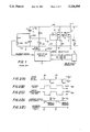
BRIEF DESCRIPTION OF THE DRAWINGS
FIG. 1, is a circuit diagram of a prior art switching circuit which includes a pair of MOSFET power switches, and which uses snubber circuitry to control the gate bias of the MOSFETS;
FIG. 2 is a series of wave forms of signals occurring throughout the circuit of FIG. 1;
FIG. 3 is circuit diagram of a switching circuit like FIG. 1, but which includes certain modifications in order to achieve the objectives of the invention;
FIG. 4 is a series of curves illustrating signals occurring throughout the circuit of FIG. 3; and
FIG. 5 is a circuit diagram of a gate drive module included in the circuits of FIGS. 1 and 3.
The circuit of FIG. 1 includes a gate drive module represented by a block 10. This module operates in a manner to respond to pulse-width modulated drive pulses (FIG. 2A) from a pulse-width modulator 12 to drive a pair of MOSFETS Q1, Q2. For that purpose, the output of the drive module (FIG. 2B) is introduced to the gate electrodes of the MOSFETS Q1, Q2 through respective 10 Ohm resistors R1 and R2.
The circuit of FIG. 1 includes a positive bias supply Zener Diode CR1, which may be of the type designated IN4744. Zener Diode CR1 is shunted by a 1 microfarad by-pass capacitor C2. The Zener diode is connected to through a 100 kilo-ohm resistor R3 to a positive potential lead 100 which is connected to the drain electrodes of MOSFETS Q1, Q2. The Zener diode is also connected to a common grounded lead 102 which, in turn, is connected to the drive module 10. The source electrodes of MOSFETS Q1 and Q2 are also connected to common grounded lead 102.
During start-up of the circuit of FIG. 1, capacitor C2 are charged, for example, to 10-15 volts through resistor R3. This is achieved before the MOSFETS Q1, Q2 turn-on because, when the MOSFETS are turned off there is substantial voltage VDS between the leads 100 and 102 (FIG. 2C), and the drive module 10 draws negligible current in the steady turned-off state of the circuit.
The circuit of FIG. 1 also includes a 0.0027 microfarad snubber capacitor C1 connected to lead 100 and to a steering diode CR2. The diode may be of the type designated MUR160. Diode CR2 is connected to a 1 microfarad capacitor C2 which, in turn, is connected to lead 102. The junction of diode CR2 and capacitor C2 is connected to the junction of resistor R3 and Zener diode CR1 and to the gate drive module 10. In this manner, positive bias (FIG. 2D) is supplied to the drive module.
The circuit of FIG. 1 also includes a 100 ohm main snubber resistor R4 which is connected to the junction of capacitor C1 and diode CR2, and which is also connected to lead 102 through a diode CR3. The diode may be of the type designated 1N4937. The cathode of the diode CR3 is connected to the gate drive module 10 to provide a sense point for the drive module.
The positive bias supply capacitor C2 is charged when the MOSFETS Q1, Q2 are turned off. At that time, a current IC1 flows through the snubber capacitor C1 and through the steering diode CR2 into capacitor C2. The direction of the current flow IC1 is shown by the arrow in FIG. 1. Capacitor C1 charges up to substantially the drain-source voltage (VDS) of the turned-off power switches Q1, Q2 (FIG. 2--curve C). Accordingly, the total charge available to the positive bias supply (CR2, CR1) is C1·VDS (off). The average available positive bias current is the aforesaid charge multiplied by the switching frequency or C1 VDS ·F) (FIG. 2--curve D).
The current drawn by the gate drive module 10 is approximately QG= gate charge per power MOSFET x the number (N) of MOSFETS x frequency (QG·N·F) where: QG is given by the manufacturer's data sheets; and N in the circuit of FIG. 1 is 2. To assure adequate positive bias current for the module 10, the average available positive bias current (C1·VDS ·F) must be greater than the current drawn by the module (QG·N·F).
As can be seen from the foregoing, increasing frequency (F) does not affect adequacy of the drive because both the supply and the demand are correspondingly increased.
When the MOSFETS power switches Q1, Q2 are turned on, the snubber capacitor C1 discharges through the main snubber resistor R4 and steering diode CR3 (FIG. 2E). The drive module uses the sense point from the cathode of diode CR3 to hold the gate drive module turned-off when the MOSFETS Q1, Q2 are supposed to be off, even when positive excursions occur on the drain electrodes of the MOSFETS.
As shown in FIG. 3, the circuit of FIG. 1 is modified in accordance with the teaching of the present invention by inserting a 1 microfarad capacitor C3, shunted by a Zener diode CR4, in series between the anode of diode CR3 and lead 102; by connecting the anode of the diode CR3 to the gate drive module 10 to supply a negative bias to the gate drive module; and by introducing a 75 ohm resistor R5 between resistor R3 and the cathode of Zener diode CR1. Zener diode CR4 may be of the type designated IN751C.
In the circuit of FIG. 3, the current flowing through the snubber resistor R4 and through diode CR3 during the turn-on of the MOSFETS power switches Q1, Q2 is caused to flow through capacitor C3 and through Zener diode CR4. This current flow generates a negative DC bias of, for example, 5.1 volts in the gate drive module 10. The steering diode CR3 prevents this negative bias from being drained away when the voltage on capacitor C1 and resistor R4 goes positive. This negative bias approximately doubles the turn-off speed of the MOSFETS power switches Q1 and Q2, which greatly reduces the size of the snubber circuit required for the power switches, and/or reduces the turn-off losses of the power switches. In the circuit under consideration it would be necessary either to double the size of the snubber circuit (raising the rating of resistor R4 to 40 watts), or to nearly double power switch dissipation (from 20 watts per switch to 35 watts per switch) if the negative bias was not employed.
Since the available charge per cycle from the snubber capacitor C1 is the same in the charging mode (turn-off) and discharging mode (turn-on), and the gate module derives the same current from both the positive bias and negative bias; if the drive bias for the positive bias is adequate, it will be sufficient for the negative bias. The only difference is that for a larger gate voltage excursion due to the negative bias, the total QG (Gate charge) is slightly larger. This affects both the positive bias and the negative bias demand equally.
When groups of the MOSFETS power switches are connected in series, adding the resistor R5 in series with the positive gate bias Zener diode CR1 helps force the balance in the turn-off voltages of the MOSFET power switching groups. If one group of MOSFETS turns off sooner than the other, it will hog all the turn-off voltage during this jump start, before the other group turns-off and shares the turn-off until the turn-off clamp is reached. For example, with snubber capacitors of 2700 picofarads and 27 amps of switch current, a 10 nano second jump start translates into a 100 volt imbalance. The group drawing the voltage can be pushed in turn-off toward their break-down voltage resulting in over stress and damage to one or more of the MOSFETS in that group.
The balancing scheme forces a turn-off delay into the MOSFET group that tends to draw the turn-off voltage, thereby forcing the MOSFETS groups to share the turn-off voltage. If one group of MOSFETS tends to draw the turn-off voltage, more current will become available to the positive bias supply of that groups' gate drive since available current is proportional to VDS (VDS C1·F). Since the gate drive demand remains relatively constant, this excessive gate bias supply current will flow through resistor R5 thereby increasing the positive bias voltage. This positive bias voltage will allow the gate electrodes to charge to the higher positive voltage. When it becomes time to turn off the MOSFETS, the additional positive bias will translate into more delay time until the gate electrodes' turn-off threshold is reached, because more capacitive charge needs to be discharged. This added delay counteracts the hogging of that group of MOSFETS, forcing all the MOSFET groups substantially to share the turn-off clamp voltage. In the existing circuit, drain-to-source turn-off voltage imbalances are reduced by more than fifty (50%) percent.
The wave forms shown in FIGS. 4A-4E, are the same as those in FIGS. 2A-2E, with the exception that the gate voltage of curve B is shifted to extend, for example, between -4 and +13 volts, instead of 0 and +15 volts as in the circuit of FIG. 1.
The gate drive module 10 of FIGS. 1 and 3, as is evident from the curves of FIGS. 2A-2E and 4A-4E, is a simple switching circuit and may take any of a variety of well known forms. One possible circuit configuration is shown in FIG. 5.
The circuit of FIG. 5 includes a turn-on transistor switch QX02 and a turn-off Darlington transistor switch QX03, QX04. A FET QX01 is included in a hold-off circuit which prevents transients from turning the switching circuit on during intervals when it is switched off.
The gate drive pulse transformer is connected between the drive pin and the gate pin of the module. A positive going pulse from the transformer turns on transistor QX02 pulling its emitter high toward + bias. The emitter of the transistor is connected to the gate pin which in turn is connected to R1 and R2 and the gates of the main FET's in FIGS. 1 and 3. The gates of the main FET's charge up to + bias through R1 and R2, thereby turning off the FET's. The transistors QX03 and QX04 in the module stay off during this time.
A negative pulse from the gate drive transformer pulls the drive pin negative with respect to the gate pin. This turns QX02 off and QX03 on which, in turn, turns QX04 on. QX04 being turned on pulls the gate pin down toward "bias return" in FIG. 1 and "negative bias" in FIG. 3. This in turn pulls the gate voltage of the main FET's to 0 in FIG. 1 and the negative bias in FIG. 3 through R1 and R2.
The FET QX01 circuit is driven off "snubber sense", and this circuit keeps the main FET's of FIGS. 1 and 2 off after a turn-off has occurred and does not effect turn-off speed. Diode CRX01 protects the gate drive circuit from inductive spikes at the end of the turn-on pulse.
The magnitude of the gate drive resistors R1 and R2 cannot be reduced below a given value in parallel MOSFET operation, without risking a destructive parasitic oscillation. The recommended minimum value for a popular type of MOSFET is 15 ohms. Hence, the speed of the MOSFET turn-off can not be increased simply by reducing the gate drive resistors' value. On a MOSFET, the turn-on and turn-off occur at a given threshold voltage, typically when the gate is biased +4 volts gate-to-source. During the turn-on, a certain amount of charge needs to be injected into the gate, and an equal amount removed during turn-off. For the above mentioned popular MOSFET this is about 50 nano-Coulombs. Now the turn-off speed can be calculated for both the circuit in FIG. 1 and FIG. 3.
In the circuit of FIG. 1, R1 and R2 are pulled down to the negative bias which can be -5 volts, for example. This means a total of 9 volts across R1 and R2. Hence, the turn-off current per transistor is 9 v divided by 15 ohms or 600 mA. The turn-off time is 50 nano Coulombs divided by 600 mA or 83 nano-seconds. This is less than half the time for the circuit in FIG. 1.
During the turn-off transistor, the power transistors see simultaneous high voltages and high currents, and hence high power consumption which is the product of voltage and current.
Therefore, the faster the power transistors go through this mode of high dissipation, the less power dissipation per switching cycle the power transistors will see. In the above example, reducing the turn-off time by more than half also reduces the turn-off power dissipation by more than half.
The invention provides, therefore, a simple and improved circuit for supplying gate drive bias for MOSFET power switches in a switched type of power supply which serves to speed up the turn-off speed of the MOSFETS, and also provides for current sharing in circuits in which more than one group of MOSFETS with different source potentials are used.
It will be appreciated that while a particular embodiment of the invention has been shown and described, modifications may be made. It is intended in the claims to cover all modifications which come within the true spirit and scope of the invention.

Claims (4)

I claim:
1. A switching circuit for a switched power supply, and the like, comprising: at least one field effect transistor having drain, source and gate electrodes, and constituting a power switch; a gate drive module having input terminals coupled to a source of drive signals, and having an output terminal connected to said gate electrode for causing said field effect transistor to turn on and off; a first bias supply network connected across said drain and source electrodes and responsive to a charging current when said field effect transistor is turned off for supplying a positive bias to said gate drive module; a second bias supply network connected across said drain and source electrodes and responsive to a charging current when said field effect transistor is turned on for supplying a negative bias to said gate drive module; and a snubber network which in turn includes a snubber capacitor connected to said drain electrode, said snubber capacitor being included in both said first and second bias supply networks, in which said snubber network includes a snubber resistor series-connected with said snubber capacitor, and said second bias supply network includes a steering diode and a Zener diode series-connected between said snubber resistor and said source electrode, and a second capacitor shunted across said Zener diode.
2. The switching circuit defined in claim 1, in which said first bias supply network includes a second steering diode connected to said snubber capacitor, a third capacitor connected between said steering diode and said source electrode, and a second Zener diode shunted across said third capacitor.
3. The switching circuit defined in claim 2, and which includes a first resistor connected across said snubber capacitor and said second steering diode.
4. The switching circuit defined in claim 3, and which includes a second resistor series connected with said first resistor and said second Zener diode.
US07/712,571 1991-06-10 1991-06-10 Gate drive bias circuit for MOSFET power switches Expired - Fee Related US5124595A (en)

Priority Applications (1)

Application Number Priority Date Filing Date Title
US07/712,571 US5124595A (en) 1991-06-10 1991-06-10 Gate drive bias circuit for MOSFET power switches

Applications Claiming Priority (1)

Application Number Priority Date Filing Date Title
US07/712,571 US5124595A (en) 1991-06-10 1991-06-10 Gate drive bias circuit for MOSFET power switches

Publications (1)

Publication Number Publication Date
US5124595A true US5124595A (en) 1992-06-23

Family

ID=24862684

Family Applications (1)

Application Number Title Priority Date Filing Date
US07/712,571 Expired - Fee Related US5124595A (en) 1991-06-10 1991-06-10 Gate drive bias circuit for MOSFET power switches

Country Status (1)

Country Link
US (1) US5124595A (en)

Cited By (13)

* Cited by examiner, † Cited by third party
Publication number Priority date Publication date Assignee Title
US5349242A (en) * 1990-11-15 1994-09-20 Kabushiki Kaisha Toshiba Bidirectional switch circuit with automatic return-current path selector
US5432471A (en) * 1992-09-04 1995-07-11 Mitsubishi Denki Kabushiki Kaisha Insulated gate semiconductor device
GB2410385A (en) * 2004-01-23 2005-07-27 Hewlett Packard Development Co Switching circuit having biasing snubber circuit
US6930473B2 (en) 2001-08-23 2005-08-16 Fairchild Semiconductor Corporation Method and circuit for reducing losses in DC-DC converters
US20050180179A1 (en) * 2004-02-17 2005-08-18 Hirst B. M. Snubber ciruit
EP1988633A1 (en) * 2007-05-03 2008-11-05 Honeywell International Inc. Integrated gate driver for controlling and protecting power modules
US20100134181A1 (en) * 2007-11-19 2010-06-03 Kinsella Barry Circuit for switchably connecting an input node and an output node
US8183892B2 (en) 2009-06-05 2012-05-22 Fairchild Semiconductor Corporation Monolithic low impedance dual gate current sense MOSFET
US20120313184A1 (en) * 2011-06-07 2012-12-13 Kabushiki Kaisha Toyota Jidoshokki Switching circuit
US8456140B2 (en) 2010-07-14 2013-06-04 Arm Limited Power control apparatus and method for controlling a supply voltage for an associated circuit
US9685947B2 (en) 2015-03-30 2017-06-20 Halliburton Energy Services, Inc. Simplified gate driver for power transistors
US9692409B2 (en) 2015-03-30 2017-06-27 Halliburton Energy Services, Inc. Simplified gate driver for power transistors
US10141923B2 (en) 2016-08-25 2018-11-27 Toyota Motor Engineering & Manufacturing North America, Inc. System and method for eliminating gate voltage oscillation in paralleled power semiconductor switches

Citations (2)

* Cited by examiner, † Cited by third party
Publication number Priority date Publication date Assignee Title
JPS61245617A (en) * 1985-04-23 1986-10-31 Mitsubishi Electric Corp Driving circuit for field effect type transistor
US4952819A (en) * 1987-04-15 1990-08-28 U.S. Philips Corporation Circuit for limiting current peaks at turn-on of a switching transistor

Patent Citations (2)

* Cited by examiner, † Cited by third party
Publication number Priority date Publication date Assignee Title
JPS61245617A (en) * 1985-04-23 1986-10-31 Mitsubishi Electric Corp Driving circuit for field effect type transistor
US4952819A (en) * 1987-04-15 1990-08-28 U.S. Philips Corporation Circuit for limiting current peaks at turn-on of a switching transistor

Cited By (20)

* Cited by examiner, † Cited by third party
Publication number Priority date Publication date Assignee Title
US5349242A (en) * 1990-11-15 1994-09-20 Kabushiki Kaisha Toshiba Bidirectional switch circuit with automatic return-current path selector
US5432471A (en) * 1992-09-04 1995-07-11 Mitsubishi Denki Kabushiki Kaisha Insulated gate semiconductor device
US6930473B2 (en) 2001-08-23 2005-08-16 Fairchild Semiconductor Corporation Method and circuit for reducing losses in DC-DC converters
GB2410385A (en) * 2004-01-23 2005-07-27 Hewlett Packard Development Co Switching circuit having biasing snubber circuit
GB2410385B (en) * 2004-01-23 2006-09-27 Hewlett Packard Development Co Snubber circuit
US20050180179A1 (en) * 2004-02-17 2005-08-18 Hirst B. M. Snubber ciruit
US8253394B2 (en) 2004-02-17 2012-08-28 Hewlett-Packard Development Company, L.P. Snubber circuit
EP1988633A1 (en) * 2007-05-03 2008-11-05 Honeywell International Inc. Integrated gate driver for controlling and protecting power modules
US20080272658A1 (en) * 2007-05-03 2008-11-06 Hassan Ali Kojori Integrated gate drive for use in control and protection of power modules
US7777370B2 (en) 2007-05-03 2010-08-17 Honeywell International Inc. Integrated gate drive for use in control and protection of power modules
US8130029B2 (en) * 2007-11-19 2012-03-06 Analog Devices, Inc. Circuit for switchably connecting an input node and an output node
US20100134181A1 (en) * 2007-11-19 2010-06-03 Kinsella Barry Circuit for switchably connecting an input node and an output node
US8183892B2 (en) 2009-06-05 2012-05-22 Fairchild Semiconductor Corporation Monolithic low impedance dual gate current sense MOSFET
US8358157B2 (en) 2009-06-05 2013-01-22 Fairchild Semiconductor Corporation Monolithic low impedance dual gate current sense MOSFET
US8456140B2 (en) 2010-07-14 2013-06-04 Arm Limited Power control apparatus and method for controlling a supply voltage for an associated circuit
US20120313184A1 (en) * 2011-06-07 2012-12-13 Kabushiki Kaisha Toyota Jidoshokki Switching circuit
US9083333B2 (en) * 2011-06-07 2015-07-14 Kabushiki Kaisha Toyota Jidoshokki Switching circuit
US9685947B2 (en) 2015-03-30 2017-06-20 Halliburton Energy Services, Inc. Simplified gate driver for power transistors
US9692409B2 (en) 2015-03-30 2017-06-27 Halliburton Energy Services, Inc. Simplified gate driver for power transistors
US10141923B2 (en) 2016-08-25 2018-11-27 Toyota Motor Engineering & Manufacturing North America, Inc. System and method for eliminating gate voltage oscillation in paralleled power semiconductor switches

Similar Documents

Publication Publication Date Title
EP1596496B1 (en) Control circuit for an insulated gate bipolar transistor (IGBT)
KR900006538B1 (en) Transformerless drive circuit for field-effect transistors
US6744224B2 (en) Rush current limiting circuit for a PFM control charge pump
JP4901445B2 (en) Drive circuit and semiconductor device using the same
US5124595A (en) Gate drive bias circuit for MOSFET power switches
US20100141304A1 (en) Drive circuit for power element
US7551004B2 (en) Inverter apparatus with improved gate drive for power MOSFET
US20050161700A1 (en) Integrated power switching circuit
US9923557B2 (en) Switching circuit and power conversion circuit
US10110222B2 (en) Drive unit
US11543846B2 (en) Gate driver circuit for reducing deadtime inefficiencies
KR20060059996A (en) High frequency control of a semiconductor switch
US9595967B2 (en) Level shift circuit and driver circuit
US7834669B2 (en) Semiconductor output circuit for controlling power supply to a load
US7701264B2 (en) Semiconductor output circuit
CN107168433B (en) Output circuit
US9318973B2 (en) Driving device
JP2020025158A (en) High breakdown voltage integrated circuit
US6717784B2 (en) Rush current suppression circuit
KR20190108785A (en) Power source converter, apparatus for driving switching element and apparatus for driving load
JP2022051278A (en) Semiconductor device
JP2009219017A (en) Load control apparatus, and method of generating input pulse therefor
US20230179195A1 (en) Multi-voltage bootstrapping drivers
WO2023032413A1 (en) Semiconductor device
US10965283B2 (en) Floating switch and drive circuit thereof

Legal Events

Date Code Title Description
AS Assignment

Owner name: PIONEER MAGNETICS, INC.,, CALIFORNIA

Free format text: ASSIGNMENT OF ASSIGNORS INTEREST.;ASSIGNOR:NABDEKCIRBM HISH;REEL/FRAME:005735/0896

Effective date: 19910606

FEPP Fee payment procedure

Free format text: PAYOR NUMBER ASSIGNED (ORIGINAL EVENT CODE: ASPN); ENTITY STATUS OF PATENT OWNER: SMALL ENTITY

FPAY Fee payment

Year of fee payment: 4

FPAY Fee payment

Year of fee payment: 8

REMI Maintenance fee reminder mailed
LAPS Lapse for failure to pay maintenance fees
FP Lapsed due to failure to pay maintenance fee

Effective date: 20040623

STCH Information on status: patent discontinuation

Free format text: PATENT EXPIRED DUE TO NONPAYMENT OF MAINTENANCE FEES UNDER 37 CFR 1.362