EP1310988A1 - Semiconductor device and method of manufacture thereof - Google Patents
Semiconductor device and method of manufacture thereof Download PDFInfo
- Publication number
- EP1310988A1 EP1310988A1 EP00940828A EP00940828A EP1310988A1 EP 1310988 A1 EP1310988 A1 EP 1310988A1 EP 00940828 A EP00940828 A EP 00940828A EP 00940828 A EP00940828 A EP 00940828A EP 1310988 A1 EP1310988 A1 EP 1310988A1
- Authority
- EP
- European Patent Office
- Prior art keywords
- semiconductor device
- insulating film
- manufacturing
- wiring
- conducting portions
- Prior art date
- Legal status (The legal status is an assumption and is not a legal conclusion. Google has not performed a legal analysis and makes no representation as to the accuracy of the status listed.)
- Granted
Links
Images




Classifications
-
- H—ELECTRICITY
- H10—SEMICONDUCTOR DEVICES; ELECTRIC SOLID-STATE DEVICES NOT OTHERWISE PROVIDED FOR
- H10P—GENERIC PROCESSES OR APPARATUS FOR THE MANUFACTURE OR TREATMENT OF DEVICES COVERED BY CLASS H10
- H10P70/00—Cleaning of wafers, substrates or parts of devices
- H10P70/20—Cleaning during device manufacture
- H10P70/27—Cleaning during device manufacture during, before or after processing of conductive materials, e.g. polysilicon or amorphous silicon layers
- H10P70/277—Cleaning during device manufacture during, before or after processing of conductive materials, e.g. polysilicon or amorphous silicon layers the processing being a planarisation of conductive layers
-
- H—ELECTRICITY
- H10—SEMICONDUCTOR DEVICES; ELECTRIC SOLID-STATE DEVICES NOT OTHERWISE PROVIDED FOR
- H10P—GENERIC PROCESSES OR APPARATUS FOR THE MANUFACTURE OR TREATMENT OF DEVICES COVERED BY CLASS H10
- H10P52/00—Grinding, lapping or polishing of wafers, substrates or parts of devices
- H10P52/40—Chemomechanical polishing [CMP]
- H10P52/403—Chemomechanical polishing [CMP] of conductive or resistive materials
-
- H—ELECTRICITY
- H10—SEMICONDUCTOR DEVICES; ELECTRIC SOLID-STATE DEVICES NOT OTHERWISE PROVIDED FOR
- H10W—GENERIC PACKAGES, INTERCONNECTIONS, CONNECTORS OR OTHER CONSTRUCTIONAL DETAILS OF DEVICES COVERED BY CLASS H10
- H10W20/00—Interconnections in chips, wafers or substrates
- H10W20/01—Manufacture or treatment
- H10W20/031—Manufacture or treatment of conductive parts of the interconnections
-
- H—ELECTRICITY
- H10—SEMICONDUCTOR DEVICES; ELECTRIC SOLID-STATE DEVICES NOT OTHERWISE PROVIDED FOR
- H10W—GENERIC PACKAGES, INTERCONNECTIONS, CONNECTORS OR OTHER CONSTRUCTIONAL DETAILS OF DEVICES COVERED BY CLASS H10
- H10W20/00—Interconnections in chips, wafers or substrates
- H10W20/40—Interconnections external to wafers or substrates, e.g. back-end-of-line [BEOL] metallisations or vias connecting to gate electrodes
- H10W20/41—Interconnections external to wafers or substrates, e.g. back-end-of-line [BEOL] metallisations or vias connecting to gate electrodes characterised by their conductive parts
- H10W20/425—Barrier, adhesion or liner layers
Definitions
- the present invention relates to a semiconductor device having a multilayer wiring structure, and to a method of manufacturing a semiconductor device having a multilayer wiring structure, which includes the steps of chemical mechanical polishing (CMP) for flattening the surface of an insulating film and the accompanying cleaning and rinsing steps.
- CMP chemical mechanical polishing
- each layer is formed with a predetermined conductor pattern.
- the conductor pattern comprises conducting portions such as metal wirings, metal plugs and pads.
- the metal plug (which comprises a metal material filled in a connection hole) functions to electrically connect two different layers to each other.
- the metal wiring needs to have a low resistance and a high anti-electromigration property. Therefore, metal wirings and plugs made of Cu or a Cu alloy, which is a good conductor and has a high anti-electromigration property, are being developed.
- the damascene process is known as a process for making metal wirings or plugs of Cu or a Cu alloy in a multilayer wiring structure.
- the technique of the damascene process is described, for example, in C.W. Kaanta et. al., VMIC Conf. Proc. 8, P.144 (1991).
- one layer including metal wirings and plugs is formed as follows. First, an insulating film is formed on a substrate, and wiring grooves for later housing metal wirings and/or connection holes for later housing plugs are formed in the insulating film by etching. Subsequently, a wiring material is deposited in the wiring grooves and the connection holes, thereby forming metal wirings and plugs in a complete product. At this time, the wiring material is deposited also at the portions on the insulating film where the wiring grooves and the connection holes are not formed. The wiring material deposited on the insulating film is removed through the polishing process by CMP.
- the polishing process flattens the insulating film so that the upper surface of the insulating film is flush with the upper surface of the metal wirings and the plugs formed in the insulating film, thereby providing predetermined conducting portions.
- the wiring grooves and the corresponding connection holes are formed individually with respect to each layer by the wiring material loading step and the following CMP step.
- the dual damascene process is also known.
- wiring grooves are formed in a first insulating film whereas connection holes opening toward the wiring grooves are formed in a second insulating film arranged under the first insulating film.
- the CMP process is performed with respect to the first insulating film.
- the surface of a substrate is polished for flattening using a slurry containing silica or alumina for example. Subsequently, the substrate surface is polished using pure water as required.
- the surface of the semiconductor substrate is contaminated by silica or alumina itself or by metal of the polished metal wirings or plugs. Such contamination of the semiconductor substrate by metallic impurity influences the electric characteristics of the semiconductor, deteriorating the reliability of the device. Therefore, a cleaning step for removing the metallic impurity from the semiconductor substrate surface need be performed after the CMP step.
- the cleaning step cleaning is performed using a predetermined chemical cleaning liquid to remove the metallic impurity on the substrate surface.
- a rinsing step is performed using pure water to remove the cleaning liquid.
- the chemical cleaning liquid needs to have a dissolving power for metal.
- the conducting portions exposed at the layer surface after the polishing step corrodes in the cleaning step due to the strong metal dissolving power of the cleaning liquid.
- JP-A-4-40270 discloses a technique in which an electronic component is cleaned using pure water of a decreased dissolved oxygen concentration. However, such cleaning using pure water cannot remove the metal contaminant after the CMP step.
- JP-A-7-60209, JP-A-10-128253 and JP-A-6-318584 each discloses a technique in which an electronic component is rinsed with pure water of a decreased dissolved oxygen concentration after the cleaning step to remove the cleaning liquid.
- the technique disclosed in these documents relates to the rinsing liquid for use after the general cleaning process of electronic components, and does not assume the existence of such a cleaning liquid having a metal dissolving power as that used in the cleaning step following the CMP step.
- JP-A-10-72594 discloses a technique for suppressing the corrosion which occurs through the cleaning step following the CMP process.
- the cleaning step is performed using a cleaning liquid containing organic acid including carboxyl group, and a complexing agent such as EDTA.
- organic acid which has a relatively low metal dissolving power, can suppress the corrosion at the surfaces of the metal wirings.
- JP-A-10-72594 owing to the existence of the complexing agent, the cleaning ability of the cleaning liquid is not degraded even by the use of organic acid having a relatively low metal dissolving power.
- the wiring material of the conducting portions is partially lost, i.e. corroded at some locations on the layer after the cleaning and rinsing steps following the CMP process.
- the inventors have found that such local metal corrosion occurs in the rinsing step, not in the cleaning step.
- Fig. 9 is a schematic view illustrating the local corrosion of a metal wiring conventionally occurred in the rinsing step. Shown in Fig. 9 is part of one layer after the CMP process and the subsequent cleaning and rinsing steps, in which a predetermined conductor pattern is formed as embedded in an insulating film 100.
- the conductor pattern comprises a pad 101, metal wirings 102, 103 and metal plugs 104 as conducting portions formed in a same layer.
- the metal wiring 102 is electrically connected to the pad 101 to provides a set of conducting portions in the conductor pattern.
- the metal wiring 102 is locally corroded at the edge portions.
- One metal wiring 103 and another metal wiring 103 are separated from each other within the same layer, but electrically connected to each other to provide another set of conducting portions. The electrical connection between these two metal wirings 103 is provided by a metal wiring 105 electrically connected to the both metal wirings 103 via the metal plugs 4 formed in the underlying layer.
- the inventors have found that local corrosion occurs at the edges of a conducting portion having a relatively large area, and at the edges of a set of conducting portions electrically connected to each other to have a relatively large area in a same layer. Specifically, as can be seen at the edges of the metal wiring 102 in Fig. 9, local corrosion develops to a considerable degree at the edges of a conducting portion having a surface area of no less than 500 ⁇ m 2 , and at the edges of a set of conducting portions electrically connected to each other to have a surface area of no less than 500 ⁇ m 2 in a same layer. The reason why the local corrosion does not occur at the edges of the metal wirings 103 of Fig.
- the set of conducting portions including the metal wirings 103 does not have a surface area of no less than 500 ⁇ m 2 in the layer shown in Fig. 9.
- the local corrosion during the rinsing step occurs even at a set of conducting portions that consists of wirings only and does not include a pad, if the set of conducting portion has a surface area of no less than 500 ⁇ m 2 in a same layer.
- Metal corrosion in an aqueous solution occurs as local cell reaction, which is the combination of cathodic reduction reaction which occurs because hydrogen ions or dissolved oxygen in the solution act on the metal surface as oxidizer, and anodic dissolution reaction in which metal is oxidized to dissolve in the aqueous solution.
- cathodic reduction reaction in which metal is oxidized to dissolve in the aqueous solution.
- the anodic dissolution reaction is represented by the formula (I)
- the cathodic reduction reaction is represented by the formula (II).
- the point where the cathodic reaction is likely to occur is called a cathodic reaction active site
- an anodic reaction active site the point where the anodic reaction is likely to occur.
- the distribution of the two kinds of active sites varies depending on the physicochemical state of the metal surface, i.e. the lattice structure and the concentration of the contacting solution and the like.
- the CMP process and the accompanying cleaning and rinsing steps are carried out using an aqueous solution. Therefore, in the case where the metal wirings are formed of Cu for example, the corrosion of the Cu wirings occurs as local cell reaction provided by the combination of the anodic reaction (I) and the cathodic reaction (II). When the anodic reaction (I) and the cathodic reaction (II) occur evenly on the surface of the wirings, the Cu wirings corrode generally uniformly. On the other hand, when each of the two kinds of reaction occurs locally, the dissolution of Cu occurs locally at the anodic reaction active sites, resulting in local corrosion, i.e. local loss of the Cu wirings.
- JP-A-10-72594 described before discloses the use of organic acid having a low metal dissolving power together with a complexing agent instead of the conventionally used inorganic acid having a high metal dissolving power. Since the driving force of the organic acid for the anodic dissolution reaction, i.e. the metal dissolving power of the organic acid is relatively low, the use of organic acid as an active ingredient of the cleaning liquid suppresses the uniform corrosion of the metal wirings.
- the conductor pattern having undergone the subsequent rinsing step suffer from local corrosion of the wiring material at a set of conducting portions electrically connected to each other to have a surface area of no less than 500 ⁇ m 2 in a same layer or at a conducting portion having a surface area of no less than 500 ⁇ m 2 , as does in the metal wiring 102 of Fig. 9.
- the concentration of the cleaning liquid remaining on the substrate surface gradually decreases to inevitably pass the ultralow concentration range, finally reaching substantially zero.
- the inventors have found that the local corrosion is likely to occur when the concentration lies in the ultralow concentration range of 4.70x10 -4 -1.96x10 -7 mol/l.
- the cleaning liquid lies in the ultralow concentration range, on the surface of a set of conducting portions electrically connected to each other to have a surface area of no less than 500 ⁇ m 2 in a same layer or of a conducting portion having a surface area of no less than 500 ⁇ m 2 , the anodic reaction active sites are localized at edges of a metal wiring, i.e.
- the reaction rate per unit area of the anodic reaction (I) is higher than that of the cathodic reaction (II), so that the dissolution reaction locally develops at the anodic reaction active sites, causing local corrosion.
- the local corrosion of the wiring material is extremely small at the edges of a set of conducting portions which are electrically connected to each other and which have a surface area smaller than 500 ⁇ m 2 in a same layer.
- a rinsing liquid may be used which contains pure water and a corrosion inhibitor such as benzotriazole added to the water.
- a corrosion inhibitor such as benzotriazole added to the water.
- the use of such a rinsing liquid suppresses the local corrosion, it provides another problem. That is, when the pure water containing a corrosion inhibitor is used in the rinsing step, only the pure water evaporates in the subsequent drying step, leaving most of the corrosion inhibitor on the surface of the semiconductor substrate.
- the corrosion inhibitor may be sandwiched between the conducting portions and the insulating film. This deteriorates the adhesion strength between the layers, causing the release of the layer at that portion. In this way, the use of corrosion inhibitor in the rinsing step causes another problem and hence is not preferable.
- An object of the present invention is to provide a method of manufacturing a semiconductor device which is capable of solving or at least alleviating the problems described above.
- Another object of the present invention is to provide a semiconductor device having a structure which is capable of solving or at least alleviating the problems described above.
- a method of manufacturing a semiconductor device having a multilayer wiring structure in which at least one insulating film is formed with a conductor pattern which includes at least one set of conducting portions electrically connected to each other comprises a polishing step for flattening the conducting portions together with the insulating film by chemical mechanical polishing, a chemical cleaning step for cleaning a flattened surface of the insulating film with a cleaning liquid, and a rising step for removing the cleaning liquid using a rinsing liquid.
- the rinsing step is performed using water with a dissolved oxygen concentration decreased to no more than 6ppm by weight as the rinsing liquid.
- a method of manufacturing a semiconductor device having a multilayer wiring structure in which at least one insulating film is formed with a conductor pattern which includes at least one set of conducting portions electrically connected to each other comprises an insulating film forming step for forming an insulating film on a substrate, a pattern forming step for forming a wiring groove and a connection hole in the insulating film, a metal film forming step for applying a metal material to the insulating film to fill the wiring groove and the connection hole with the metal material, a polishing step for polishing the metal film by chemical mechanical polishing so that the metal material filled in the wiring groove and the connectionhole remains as conducting portions, a cleaning step for cleaning the polished insulating film with a cleaning liquid, a rinsing step for removing the cleaning liquid with water with a dissolved oxygen concentration of no more than 6ppm by weight, and a drying step for removing the water used in the rinsing step.
- the dissolved oxygen concentration of the water as the rinsing liquid is no more than 4ppm by weight.
- the conductor pattern is formed of Cu or a Cu alloy.
- the set of conducting portions has a surface area of no less than 500 ⁇ m 2 .
- the set of conducting portions includes a pad, and a wiring directly connected to the pad.
- the set of the conducting portions of the one insulating film includes a plurality of wirings which are electrically connected to each other via a conductor pattern of an underlying insulating film.
- the set of the conducting portions may be made up of several bent or branched portions of a single wiring.
- the wiring of the conducting portions has a width of no more than 1.0 ⁇ m.
- the cleaning liquid used in the cleaning step includes at least one of organic acid, inorganic acid and alkali. More preferably, at least one organic acid is selected from the group consisting of oxalic acid, malonic acid, succinic acid, glutaric acid, adipic acid, maleic acid, fumaric acid, tartaric acid, citric acid, malic acid, acetic acid, salicylic acid.
- the inorganic acid may be diluted hydrofluoric acid, and the alkali may be ammonia.
- the cleaning liquid may further contain a surface-active agent.
- the surface-active agent is ammonium dodecylsulfonate and/or n-ammonium dodecylbenzenesulfonate.
- the polishing step includes a first polishing treatment using a chemical slurry and a second polishing treatment using water with a dissolved oxygen concentration decreased to no more than 6ppm by weight. More preferably, the dissolved oxygen concentration of the water used in the second polishing treatment is no more than 4ppm by weight.
- the chemical slurry is a mixture of organic acid, inorganic acid, a complexing agent and abrasive grain.
- the local corrosion which conventionally occurred in the rinsing step accompanying the chemical cleaning step after the CMP step, can be prevented by decreasing the dissolved oxygen concentration in the rinsing liquid.
- the cathodic reaction (II) is suppressed so that the anodic reaction (I) is also suppressed. Therefore, the local loss of the Cu wiring can be prevented even when the concentration of the cleaning liquid remaining on the substrate surface lies in the ultralow concentration range during the rinsing step and the potential anodic reaction active sites are localized at the edges of the Cu wiring.
- the use of pure water of a decreased dissolved oxygen concentration as the polishing liquid in the second polishing treatment in the CMP step makes it possible to prevent the local loss of the metal wiring.
- a semiconductor device having a multilayer wiring structure comprising a plurality of laminated insulating films each of which is formed with a conductor pattern, the conductor pattern on each of the insulating films including a plurality of conducting portions.
- each of the conducting portions or each set of conducting portions electrically connected to each other in a same insulating layer has a surface area of no more than 500 ⁇ m 2 .
- the conductor pattern is formed of Cu or a Cu alloy.
- the conductor pattern on each of the insulating films includes a wiring having a width of no more than 1.0 ⁇ m.
- the local corrosion at conducting portions can be prevented without using pure water of a decreased dissolved oxygen concentration in the rinsing step and the second polishing step.
- the local corrosion of a conducting portion in the rinsing step and the second polishing step occurs conspicuously at the edges of a conducting portion having a surface area of no less than 500 ⁇ m 2 or at the edges of conducting portions electrically connected to each other to have a surface area of no less than 500 ⁇ m 2 in a same layer. Therefore, such local corrosion can be prevented when each of the conducting portions or each set of conducting portions electrically connected to each other has a surface area of no more than 500 ⁇ m 2 in a same insulating layer.
- the reaction rate per unit area does not differ largely between the anodic reaction (I) and the cathodic reaction (II). Therefore, the local cell reaction and the resulting corrosion hardly occur.
- the local corrosion provides a significant problem when the wiring of the conducting portion has a width of no more than 1 ⁇ m, because the proportion of the lost wiring material is large when the wiring has a width of no more than 1 ⁇ m.
- Fig. 1 is a flow chart of a multilayer wiring structure manufacturing process utilized in the present invention.
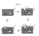
- Fig. 2 is a sectional view of a wafer during the multilayer wiring structure manufacturing process shown in Fig. 1.
- the multilayer wiring structure is formed by the dual damascene process as described below.
- a wafer 1 which has undergone the transistor making step, is subjected to an interlayer making step 10.
- an insulating film 2 as an interlayer is formed on the wafer 1.
- wiring grooves 3 for later housing metal wirings are formed in the insulating film 2
- connection holes 4 for later housing plugs are formed in an insulating film 2' lying under the insulating film 2.
- barrier films 5 are formed on the surfaces of the wiring grooves 3 and the connection holes 4, and then seed cu films (not shown) are formed on the surfaces of the barrier films 5.
- the barrier films 5 are provided to prevent Cu, which will be later formed thereon as a film, from diffusing in the insulating film 2.
- the seed cu films are necessary in the following plating step.
- Cu as a wiring material is deposited in the wiring grooves 3 and connection holes 4 to form Cu wirings 6 and Cu plugs 7 in a completed product.
- the wiring material is deposited also at portions on the insulating film 2 which are not formed with the wiring grooves 3. Therefore, as viewed entirely, a metal film 8 is formed on the insulating film.
- the unnecessary portion removing step 50 includes a CMP step 501, a chemical cleaning step 502, a rinsing step 503 and a drying step 504, which will be described later.
- the embedded wirings i.e. conducting portions are formed.
- a conductor pad may be formed in the same layer from the wiring material.
- the conductor pad may separately be formed as a bonding pad from another metal material.
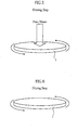
- Fig. 3 illustrates the CMP step 501 included in the unnecessary portion removing step 50 shown in Fig. 1.
- the wafer 1 as an object to be polished is secured to a polishing head 51 and is pressed against a platen 53 provided with a polishing cloth on the surface thereof.
- the polishing head 51 and the platen 53 are rotated while pouring a polishing liquid from a polishing liquid feed port 54, thereby polishing the surface of the wafer 1 for flattening.
- a pressure of 2-6psi for example is applied between the wafer 1 and the polishing cloth 52, and the polishing head 51 and the platen 53 are rotated in the same direction at 50-100rpm for example.
- the polishing cloth 52 is formed with grooves in the form of a lattice or concentric circles, which enables the polishing of the surface of the wafer 1.
- the CMP step in this embodiment comprises chemical slurry polishing and pure water polishing.
- the wafer 1 is polished using a chemical slurry as the polishing liquid.
- the chemical slurry is supplied from the polishing liquid feed port 54 to a generally central portion of the platen 53 at a flow rate of 100-200ml/min.
- the chemical slurry may be a solution containing quinaldinic acid, lactic acid, colloidal silica (abrasive grain) and hydrogen peroxide.
- the chemical slurry may further contain benzotriazole as a corrosion inhibitor.
- the wafer 1 is polished using pure water with a dissolved oxygen concentration decreased to no more than 6ppm by weight, preferably no more than 4ppm by weight as the polishing liquid.
- the pure water is supplied from a polishing liquid feed port 55 to a generally central portion of the platen 53 at a flow rate of 200-1500ml/min. This polishing prevents the local corrosion of the metal wirings.
- To decrease the dissolved oxygen concentration in the pure water use may be made of vacuum degassing, membrane vacuum degassing, thermal degassing, or bubbling of inert gas such as nitrogen or argon, for example.
- the dissolved oxygen concentration may be decreased also by adding methyl ethyl ketoxime, hydrazine, erythorbic acid, hydroquinone or the like to the pure water.
- Fig. 4 illustrates the chemical cleaning step 502 subsequent to the CMP step shown in Fig. 3.
- the chemical cleaning step 502 is carried out to remove metal contaminant or abrasive grain contaminant on the wafer 1 generated in the CMP step 501.
- the wafer 1 rotating at high speed is sandwiched between a pair of rotary brushes 61 formed of polyvinyl alcohol (PVA) and rotating at high speed for brushing.
- PVA polyvinyl alcohol
- the cleaning liquid contains one or more active ingredients selected from organic acids such as oxalic acid, malonic acid, succinic acid, glutaric acid, adipic acid, maleic acid, fumaric acid, tartaric acid, citric acid, malic acid, acetic acid or salicylic acid, inorganic acid such as dilutedhydrofluoric acid, and alkali such as ammonia.
- the cleaning liquid may contain a surface-active agent such as ammonium dodecylsulfonate or n-ammonium dodecylbenzenesulfonate.
- the cleaning liquid may contain a complexing agent such as EDTA.
- pure water is supplied to the wafer through the same rotary brushes 61 for performing rinsing treatment to rinse off the cleaning liquid as the final treatment in the chemical cleaning step 502.
- the water used for the rinse treatment may have a dissolved oxygen concentration of no more than 6ppm by weight and preferably no more than 4ppm by weight, for example.
- the rinse treatment using the rotary brushes 61 is stopped before the concentration of the cleaning liquid reaches the ultralow concentration range.
- the rinse treatment need not necessarily be performed.
- Fig. 5 illustrates the rinsing step 503 subsequent to the chemical cleaning step 502 shown in Fig. 4.
- pure water having a dissolved oxygen concentration of no more than 6ppm by weight, preferably no more than 4ppm by weight is supplied to the rotating wafer 1 from above through a rinsing liquid feed port 71. Because of the reasons described above, the use of water having a decreased dissolved oxygen concentration makes it possible to prevent the local corrosion of the metal wirings even when the concentration of the cleaning liquid passes the ultralow concentration range of 4.70x10 -4 -1.96x10 -7 mol/l.
- the dissolved oxygen concentration of the pure water may be decreased in the same manner as that of the pure water used in the pure water polishing in the CMP step 501.
- the rinsing step 503 completes when the concentration of the cleaning liquid in the rinsing liquid reaches substantially zero.
- Fig. 6 illustrates the drying step 504 subsequent to the rinsing step 503 shown in Fig. 5.
- the wafer is heated with a heater (not shown) disposed above the wafer 1 while rotating the wafer at high speed. In this way, the pure water used in the rinsing step 503 is evaporated, thereby drying the wafer.
- the surface of the wafer 1 is sufficiently flattened while preventing the metal corrosion.
- the wafer 1 treated in this way can be subjected to the interlayer making step 10 for forming wirings in the next layer.
- Fig. 7 is a plan view showing a multilayer wiring structure of a semiconductor device according to another embodiment of the present invention.
- Fig. 8 is a sectional view taken along lines VIII-VIII in Fig. 7.
- the semiconductor device having a multilayer wiring structure includes a plurality of insulating films 70, 71, 72 (See Fig. 8).
- each of the insulating film 70, 71, 72 is formed with a plurality of pads (only one shown), a plurality of wirings 74, and a plurality of connection holes 75 (metal plugs) .
- the insulating films differ from each other in formation pattern of the pads 73, the wirings 74 and the connection holes 75.
- Each of the pads 73 in each insulating film (for example, in the insulating film 70) is separated from all the wirings 74 of the same layer (See Fig. 8), but is electrically connected, via the connection hole 75 formed in the adjacent insulating film (for example, the insulating film 71), to one of the wirings 74 of another insulating film (for example, the insulating film 72).
- each of the pads 73 is not connected to any of the wirings 74 in the same insulating film. Moreover, the total surface area of the conducting portions electrically connected to each other is no more than 500 ⁇ m 2 in the same layer. Therefore, even when pure water having a relatively high dissolved oxygen concentration is used in the rinsing step, causing corrosion by the cell reaction due to the localization of anodes and cathodes respectively at the edges and at other portions of the pad 73 as a conducting portion, such corrosion does not provide a significant problem, because the ratio of the loss of the wirings relative to the conductive volume of the pad is small.
- the present invention is particularly effective in forming a Cu or Cu alloy wiring having a width of no more than 1.0 ⁇ m. This is because, when the wiring has a width of no more than 1.0 ⁇ m, the local corrosion provides a large influence. Particularly when the wiring has a width of no more than 0.5 ⁇ m, the local corrosion causes a serious problem.
- Cu wirings having a width of 1.0, 0.5 and 0.27 ⁇ m were used.
- the existence or nonexistence of local corrosion is checked with respect to each of a set of conducting portions electrically connected to each other to have a surface area of no less than 500 ⁇ m 2 in a same layer.
- the set of conducting portions having a surface area of no less than 500 ⁇ m 2 consisted of a pad, and a wiring electrically connected to the pad.
- the evaluation was performed by checking whether local corrosion occurred at the edges of the wiring. The same phenomenon occurs even at another type of conducting portion set if only the set of conducting portions has a surface area of no less than 500 ⁇ m 2 .
- wafers 1 were cleaned using cleaning liquids each containing a single kind of reagent at a predetermined concentration. Then, in the rinsing step 503, the wafers 1 were rinsed using pure water of a decreased dissolved oxygen concentration.
- oxalic acid for the single kind of reagent in each cleaning liquid, use was made of oxalic acid, malonic acid, succinic acid, glutaric acid, adipic acid, maleic acid, fumaric acid, tartaric acid, citric acid, malic acid, acetic acid or salicylic acid which are organic acids, diluted hydrofluoric acid which is inorganic acid, or aqueous ammonia which is alkali.
- the decrease of the dissolved oxygen concentration of the pure water for the rinsing step 503 was performed by membrane vacuum degassing or bubbling of inert gas (nitrogen or argon) to the concentration range of 1-4ppm by weight.
- Table 1 shows the resulting surface condition of the Cu wirings on each of the wafers which were dried in the drying step 504 after having undergone the above-described chemical cleaning step 502 and rinsing step 503.
- local corrosion of the wiring material i.e. local loss was not found at the edges of the Cu wiring of the set of conducting portions electrically connected to each other to have a surface area of no less than 500 ⁇ m 2 in a same layer.
- the wafers 1 cleaned with the cleaning liquid containing oxalic acid did not suffer from local corrosion both when the rinsing was performed using pure water whose dissolved oxygen concentration was decreased by membrane vacuum degassing and when the rinsing was performed using pure water whose dissolved oxygen concentration was decreased by bubbling of nitrogen gas.
- wafers 1 were cleaned using cleaning liquids each containing oxalic acid, malonic acid, succinic acid, glutaric acid or citric acid at a predetermined concentration, and ammonium dodecylsulfonate or n-ammonium dodecylbenzenesulfonate as a surface-active agent at the concentration of 200ppm by weight. Then, in the rinsing step 503, the wafers 1 were rinsed using pure water whose dissolved oxygen concentration was decreased to 1 or 2ppm by weight by membrane vacuum degassing.
- Table 2 shows the resulting surface condition of the Cu wiring on each of the wafers which were dried in the drying step 504 after having undergone the above-described chemical cleaning step 502 and rinsing step 503.
- local loss of the wiring material was not found at the edges of the Cu wiring of the set of conducting portions electrically connected to each other to have a surface area of no less than 500 ⁇ m 2 in a same layer.
- the decrease of the dissolved oxygen concentration was performed by membrane vacuum degassing in this example, such a decrease of dissolved oxygen concentration may be performed by bubbling of nitrogen gas or argon gas.
- each of the seven wafers was immersed in a corresponding kind of liquid for 30 minutes. Specifically, each wafer was immersed in a solution prepared by diluting a cleaning liquid containing the reagent used for that wafer in the chemical cleaning step 502 with pure water of a decreased dissolved oxygen concentration. The dissolved oxygen concentration of the pure water for the dilution was decreased by bubbling of nitrogen gas.
- Table 3 shows the resulting surface condition of the Cu wiring on each of the wafers which were dried after having undergone such immersion. In the wafers after these process steps, local loss of the wiring material was not found at the edges of the Cu wiring of the set of conducting portions electrically connected to each other to have a surface area of no less than 500 ⁇ m 2 in a same layer.
- each of the three wafers was immersed in a corresponding kind of liquid for 30 minutes. Specifically, each wafer was immersed in a solution prepared by diluting a cleaning liquid containing the reagent used for that wafer in the chemical cleaning step 502 with pure water of a decreased dissolved oxygen concentration. The dissolved oxygen concentration of the pure water for the dilution was decreased by bubbling of nitrogen gas.
- Table 4 shows the resulting surface condition of the Cu wiring on each of the wafers which were dried in the drying step 504 after having undergone such immersion. In the wafers after these process steps, local loss of the wiring material was not found at the edges of the Cu wiring of the set of conducting portions electrically connected to each other to have a surface area of no less than 500 ⁇ m 2 in a same layer.
- the pure water polishing in the CMP step 501 was performed using pure water whose dissolved oxygen concentration was decreased to no more than 1ppm as the polishing liquid.
- the dissolved oxygen concentration of the pure water was decreased by membrane vacuum degassing. After the pure water polishing and the subsequent drying step 504, an upper layer was laminated.
- the resulting surface condition of the Cu wiring on the wafer after the CMP step 501 and the drying step 504 is given in Table 5.
- Table 5 The resulting surface condition of the Cu wiring on the wafer after these process steps, local loss of the wiring material was not found at the edges of the Cu wiring of the set of conducting portions electrically connected to each other to have a surface area of no less than 500 ⁇ m 2 in a same layer.
- Table 5 Also given in Table 5 is the state of adhesion between Cu and the interlayer insulating film when the upper layer is laminated. The release of the laminated layer did not occur.
- a wiring pattern in which conducting portions electrically connected to each other, including a wiring of a width of no more than 1.0 ⁇ m, had a surface area of no more than 500 ⁇ m 2 in a same layer.
- the rinsing step was performed using pure water whose dissolved oxygen concentration was not decreased.
- wafers 1 were cleaned using cleaning liquids each containing a single kind of reagent at a predetermined concentration. Then, in the rinsing step 503, the wafers 1 were rinsed using pure water whose dissolved oxygen concentration was not decreased.
- oxalic acid for the single kind of reagent in each cleaning liquid, use was made of oxalic acid, malonic acid, succinic acid, glutaric acid, adipic acid, maleic acid, fumaric acid, tartaric acid, citric acid, malic acid, acetic acid or salicylic acid which are organic acids, diluted hydrofluoric acid which is inorganic acid, or aqueous ammonia which is alkali.
- Table 6 shows the resulting surface condition of the Cu wiring on each of the wafers which were dried in the drying step 504 after having undergone the above-described chemical cleaning step 502 and rinsing step 503.
- local corrosion of the wiring material i.e. local loss was found at the edges of the Cu wiring of the set of conducting portions electrically connected to each other to have a surface area of no less than 500 ⁇ m 2 in a same layer.
- wafers 1 were cleaned using cleaning liquids each containing a combination of reagents as given in Table 7, similarly to Example 2. Then, in the rinsing step 503, the wafers 1 were rinsed using pure water whose dissolved oxygen concentration was not decreased.
- Table 7 shows the resulting surface condition of the Cu wiring on each of the wafers which were dried in the drying step 504 after having undergone the above-described chemical cleaning step 502 and rinsing step 503.
- local loss of the wiring material was found at the edges of the Cu wiring of the set of conducting portions electrically connected to each other to have a surface area of no less than 500 ⁇ m 2 in a same layer.
- Example 3 similarly to Example 3, seven kinds of wafers were selected from the semiconductor devices provided with exposed Cu wirings which did not suffer from local loss even after having undergone the process steps under the condition of Example 1. Each of the seven wafers was immersed in a corresponding kind of liquid for 30 minutes. Specifically, each wafer was immersed in a solution prepared by diluting a cleaning liquid containing the reagent used for that wafer in the chemical cleaning step 502 with pure water whose dissolved oxygen concentration was not decreased.
- Table 8 shows the resulting surface condition of the Cu wiring on each of the wafers which were dried after having undergone such immersion. In the wafers after these process steps, local loss of the wiring material was found at the edges of the Cu wiring of the set of conducting portions electrically connected to each other to have a surface area of no less than 500 ⁇ m 2 in a same layer.
- Example 2 similarly to Example 4, three kinds of wafers were selected from the semiconductor devices provided with exposed Cu wirings which did not suffer from local loss even after having undergone the process steps under the condition of Example 2.
- Each of the three wafers was immersed in a corresponding kind of liquid for 30 minutes. Specifically, each wafer was immersed in a solution prepared by diluting a cleaning liquid containing the reagent used for that wafer in the chemical cleaning step 502 with pure water whose dissolved oxygen concentration was not decreased.
- Table 9 shows the resulting surface condition of the Cu wiring on each of the wafers which were dried after having undergone such immersion. In the wafers after these process steps, local loss of the wiring material was found at the edges of the Cu wiring of the set of conducting portions electrically connected to each other to have a surface area of no less than 500 ⁇ m 2 in a same layer.
- the pure water polishing in the CMP step 501 was performed using pure water whose dissolved oxygen concentration was not decreased.
- the resulting surface condition of the Cu wiring after such CMP step 501 and the drying step 504 is given in Table 5.
- local loss of the wiring material was found at the edges of the Cu wiring of the set of conducting portions electrically connected to each other to have a surface area of no less than 500 ⁇ m 2 in a same layer.
- the pure water polishing in the CMP step 501 was performed using pure water whose dissolved oxygen concentration was not decreased but which contained benzotriazole as a corrosion inhibitor at the concentration of 500ppm by weight.
- the resulting surface condition of the Cu wiring on the wafer dried after such CMP step 501 is given in Table 5.
- local loss of the wiring material was not found at the edges of the Cu wiring of the set of conducting portions electrically connected to each other to have a surface area of no less than 500 ⁇ m 2 in a same layer.
- adhesion failure occurred between Cu and the interlayer insulating film, resulting in the release of the laminated layer.
- a wiring pattern in which conducting portions electrically connected to each other, including a wiring of a width of no more than 1.0 ⁇ m, had a surface area of no more than 600 ⁇ m 2 in a same layer.
- the rinsing step in the unnecessary portion removing step 50 was performed using pure water whose dissolved oxygen concentration was not decreased as the rinsing liquid.
- pure water of a decreased dissolved oxygen concentration is used as the polishing liquid in the pure water polishing in the CMP step.
- the dissolved oxygen concentration is no more than 6ppm by weight, but further lower concentration is preferable. It is preferable that the dissolved oxygen concentration is no more than 4ppm by weight.
- pure water of a decreased dissolved oxygen concentration is used as the rinsing liquid in the rinsing step after the cleaning step performed accompanying the CMP step. This prevents local corrosion, i.e. local loss of a Cu or Cu alloy wiring at the edges of the conducting portions electrically connected to each other to have a surface area of no less than 500 ⁇ m 2 in a same layer.
- a conductor pattern is formed in which a wiring has a width of no more than 1.0 ⁇ m and each of the conducting portions electrically connected to each other has a surface area of no more than 500 ⁇ m 2 in a same layer.
Landscapes
- Internal Circuitry In Semiconductor Integrated Circuit Devices (AREA)
- Cleaning Or Drying Semiconductors (AREA)
- Mechanical Treatment Of Semiconductor (AREA)
Abstract
Description
| Reagent in Cleaning Liquid (Concentration) | Dissolved Oxygen Concentration in Pure Water for Rinsing /ppm by weight | Influences on Cu Wiring | ||
| Membrane Degassing | Bubbling by Inert Gas | |||
| N2 | Ar | |||
| Oxalic acid (0.7x10⁻²mol/l) | 1 | 1 | --- | No Loss |
| Malonic acid (1.2x10⁻²mol/l) | 2 | 1 | --- | No Loss |
| Succinic acid (1.0x10⁻²mol/l) | 1 | 2 | --- | No Loss |
| Glutaric acid (1.8x10⁻²mol/l) | 1 | 1 | --- | No Loss |
| Adipic acid (2.5x10⁻²mol/l) | 3 | --- | 1 | No Loss |
| Maleic acid (1.7x10⁻²mol/l) | 2 | --- | 2 | No Loss |
| Fumaric acid (1.6x10⁻²mol/l) | 1 | --- | 2 | No Loss |
| Tartaric acid (3.5x10⁻²mol/l) | 3 | --- | 2 | No Loss |
| Citric acid (1.6x10⁻²mol/l) | 2 | 1 | --- | No Loss |
| Malic acid (0.9x10⁻²mol/l) | 4 | 1 | --- | No Loss |
| Acetic acid (1.9x10⁻²mol/l) | 2 | 1 | --- | No Loss |
| Salicylic acid (1.1x10⁻²mol/l) | 1 | --- | 2 | No Loss |
| Glutaric acid (2.5x10⁻²mol/l) | 1 | 2 | --- | No Loss |
| DHF (0.5wt%) | --- | --- | 1 | No Loss |
| NH3aq (0.6x10⁻²mol/l) | --- | --- | 1 | No Loss |
| Reagent in Cleaning Liquid (Concentration) | Dissolved Oxygen Concentration in Pure water for Rinsing /ppm by weight (Membrane Degassing) | Influences on Cu Wiring |
| Oxalic acid (0.8x10⁻²mol/l) Ammonium dodecylsulfonate (200ppm) | 1 | No Loss |
| Malonic acid (1.2x10⁻²mol/l) Ammonium dodecylsulfonate (200ppm) | 2 | No Loss |
| Succinic acid (1.6x10⁻²mol/l) n-ammonium dodecylbenzenesulfonate (200ppm) | 1 | No Loss |
| Glutaric acid (1.6x10⁻²mol/l) n-ammonium dodecylbenzenesulfonate (200ppm) | 1 | No Loss |
| Citric acid (1.5x10⁻²mol/l) n-ammonium dodecylbenzenesulfonate (200ppm) | 1 | No Loss |
| Reagent in Cleaning Liquid (Concentration) | Rate of Dilution | Dissolved Oxygen Concentration in Pure water for Rinsing /ppm by weight (Bubbling by N2 gas) | Influences on Cu Wiring |
| Oxalic acid (0.8x10⁻²mol/l) | 10000 | 1 | No Loss |
| Malonic acid (1.2x10⁻²mol/l) | 1000 | 2 | No Loss |
| Citric acid (1.6x10⁻²mol/l) | 5000 | 1 | No Loss |
| Malic acid (0.9x10⁻²mol/l) | 300 | 2 | No Loss |
| Tartaric acid (3.5x10⁻²mol/l) | 8000 | 3 | No Loss |
| DHF (0.5 wt%) | 80000 | 1 | No Loss |
| NH3 aq (0.6x10⁻²mol/l) | 30000 | 1 | No Loss |
| Reagent in Cleaning Liquid (Concentration) | Rate of Dilution | Dissolved Oxygen Concentration in Pure water for Rinsing /ppm by weight (Bubbling by N2 gas) | Condition of Cu Wiring |
| Oxalic acid (0.8x10⁻²mol/l) Ammonium dodecylsulfonate (200ppm) | 500 | 1 | No Loss |
| Malonic acid (1.2x10⁻²mol/l) Ammonium dodecylsulfonate (200ppm) | 50000 | 2 | No Loss |
| Citric acid (1.5x10⁻²mol/l) n-ammonium dodecylbenzenesulfonate (200ppm) | 10000 | 1 | No Loss |
| Performed Example | Influences on Cu Wiring | Release of Laminated Layer |
| Example 5 | No Loss | Not found |
| Example 6 | No Loss | --- |
| Comparative Example 5 | Local Loss Found | --- |
| Comparative Example 6 | No Loss | Found |
| Comparative Example 7 | Local Loss Found | --- |
| Reagent in Cleaning Liquid (Concentration) | Dissolved Oxygen Concentration in Pure water for Rinsing /ppm by weight | Influences on Cu Wiring Pattern |
| Oxalic acid (0.7x10⁻²mol/l) | 8 | Local Loss Found |
| Malonic acid (1.2x10⁻²mol/l) | 8 | Local Loss Found |
| Succinic acid (1.0x10⁻²mol/l) | 9 | Local Loss Found |
| Glutaric acid (1.8x10⁻²mol/l) | 8 | Local Loss Found |
| Adipic acid (2.5x10⁻²mol/l) | 9 | Local Loss Found |
| Maleic acid (1.7x10⁻²mol/l) | 8 | Local Loss Found |
| Fumaric acid (1.6x10⁻²mol/l) | 8 | Local Loss Found |
| Tartaric acid (3.5x10⁻²mol/l) | 8 | Local Loss Found |
| Citric acid (1.6x10⁻²mol/l) | 9 | Local Loss Found |
| Malic acid (0.9x10⁻²mol/l) | 9 | Local Loss Found |
| Acetic acid (1.9x10⁻²mol/l) | 9 | Local Loss Found |
| Salicylic acid (1.1x10⁻²mol/l) | 8 | Local Loss Found |
| Glutaric acid (2.5x10⁻²mol/l) | 8 | Local Loss Found |
| DHF (0.5 wt%) | 8 | Local Loss Found |
| NH3 aq (0.6x10⁻²mol/l) | 8 | Local Loss Found |
| Reagent in Cleaning Liquid (Concentration) | Dissolved Oxygen Concentration in Pure water for Rinsing /ppm by weight | Influences on Cu Wiring |
| Oxalic acid (0.8x10⁻²mol/l) Ammonium dodecylsulfonate (200ppm) | 9 | Local Loss Found |
| Malonic acid (1.2x10⁻²mol/l) Ammonium dodecylsulfonate (200ppm) | 8 | Local Loss Found |
| Succinic acid (1.6x10⁻²mol/l) n-ammonium dodecylbenzenesulfonate (200ppm) | 8 | Local Loss Found |
| Glutaric acid (1.6x10⁻²mol/l) n-ammonium dodecylbenzenesulfonate (200ppm) | 8 | Local Loss Found |
| Citric acid (1.5x10⁻²mol/l) n-ammonium dodecylbenzenesulfonate (200ppm) | 8 | Local Loss Found |
| Reagent in Cleaning Liquid (Concentration) | Rate of Dilution | Dissolved Oxygen Concentrationin Pure water for Rinsing /ppm by weight | Influences on Cu Wiring |
| Oxalic acid (0.8x10⁻²mol/l) | 10000 | 8 | Local Loss Found |
| Malonic acid (1.2x10⁻²mol/l) | 1000 times | 9 | Local Loss Found |
| Citric acid (1.6x10⁻²mol/l) | 5000 times | 9 | Local Loss Found |
| Malic acid (0.9x10⁻²mol/l) | 300 times | 9 | Local Loss Found |
| Tartaric acid (3.5x10⁻²mol/l) | 8000 | 8 | Local Loss Found |
| DHF (0.5 wt%) | 80000 | 8 | Local Loss Found |
| NH3 aq (0.6x10⁻²mol/l) | 30000 | 8 | Local Found Loss Found |
| Reagent in Cleaning Liquid (Concentration) | Rate of Dilution | Dissolved Oxygen Concentration in Pure water for Rinsing /ppm by weight | Influences on Cu Wiring |
| Oxalic acid (0.8x10⁻²mol/l) Ammonium dodecylsulfonate (200ppm) | 500 | 8 | Local Loss Found |
| Malonic acid (1.2x10⁻²mol/l) Ammonium dodecylsulfonate (200ppm) | 50000 | 8 | Local Loss Found |
| Citric acid (1.5x10⁻²mol/l) n-ammonium dodecylbenzenesulfonate (200ppm) | 10000 | 8 | Local Loss Found |
Claims (23)
- A method of manufacturing a semiconductor device having a multilayer wiring structure in which at least one insulating film is formed with a conductor pattern which includes at least one set of conducting portions electrically connected to each other, the method comprising:wherein the rinsing step is performed using water with a dissolved oxygen concentration decreased to no more than 6ppm by weight as the rinsing liquid.a polishing step for flattening the conducting portions together with the insulating film by chemical mechanical polishing;a chemical cleaning step for cleaning a flattened surface of the insulating film with a cleaning liquid; anda rising step for removing the cleaning liquid using a rinsing liquid;
- The method of manufacturing a semiconductor device according to claim 1, wherein the dissolved oxygen concentration of the water as the rinsing liquid is no more than 4ppm by weight.
- The method of manufacturing a semiconductor device according to claim 1, wherein the conductor pattern is formed of Cu or a Cu alloy.
- The method of manufacturing a semiconductor device according to claim 1, wherein the set of conducting portions has a surface area of no less than 500µm2.
- The method of manufacturing a semiconductor device according to claim 4, wherein the set of conducting portions includes a pad, and a wiring directly connected to the pad.
- The method of manufacturing a semiconductor device according to claim 5, wherein the wiring of the conducting portions has a width of no more than 1.0µm.
- The method of manufacturing a semiconductor device according to claim 4, wherein the set of the conducting portions of the one insulating film includes a plurality of wirings which are electrically connected to each other via a conductor pattern of an underlying insulating film.
- The method of manufacturing a semiconductor device according to claim 7, wherein each of the wirings has a width of no more than 1.0µm.
- The method of manufacturing a semiconductor device according to claim 1, wherein the polishing step includes a first polishing treatment using a chemical slurry and a second polishing treatment using water with a dissolved oxygen concentration decreased to no more than 6ppm by weight.
- The method of manufacturing a semiconductor device according to claim 9, wherein the dissolved oxygen concentration of the water used in the second polishing treatment is no more than 4ppm by weight.
- A method of manufacturing a semiconductor device having a multilayer wiring structure in which at least one insulating film is formed with a conductor pattern which includes at least one set of conducting portions electrically connected to each other, the method comprising:an insulating film forming step for forming an insulating film on a substrate;a pattern forming step for forming a wiring groove and a connection hole in the insulating film;a metal film forming step for applying a metal material to the insulating film to fill the wiring groove and the connection hole with the metal material;a polishing step for polishing the metal film by chemical mechanical polishing so that the metal material filled in the wiring groove and the connection hole remains as conducting portions;a cleaning step for cleaning the polished insulating film with a cleaning liquid;a rinsing step for removing the cleaning liquid with water with a dissolved oxygen concentration of no more than 6ppm by weight; anda drying step for removing the water used in the rinsing step.
- The method of manufacturing a semiconductor device according to claim 11, wherein the dissolved oxygen concentration of the water as the rinsing liquid is no more than 4ppm by weight.
- The method of manufacturing a semiconductor device according to claim 11, wherein the metal material is Cu or a Cu alloy.
- The method of manufacturing a semiconductor device according to claim 11, wherein the set of conducting portions has a surface area of no less than 500µm2.
- The method of manufacturing a semiconductor device according to claim 14, wherein the set of conducting portions includes a pad, and a wiring directly connected to the pad.
- The method of manufacturing a semiconductor device according to claim 15, wherein the wiring of the conducting portions has a width of no more than 1.0µm.
- The method of manufacturing a semiconductor device according to claim 14, wherein the set of the conducting portions of the one insulating film includes a plurality of wirings which are electrically connected to each other via a conductor pattern of an underlying insulating film.
- The method of manufacturing a semiconductor device according to claim 17, wherein each of the wirings has a width of no more than 1.0µm.
- The method of manufacturing a semiconductor device according to claim 11, wherein the polishing step includes a first polishing treatment using a chemical slurry and a second polishing treatment using water with a dissolved oxygen concentration decreased to no more than 6ppm by weight.
- The method of manufacturing a semiconductor device according to claim 19, wherein the dissolved oxygen concentration of the water used in the second polishing treatment is no more than 4ppm by weight.
- A semiconductor device having a multilayer wiring structure comprising:a plurality of laminated insulating films each of which is formed with a conductor pattern;the conductor pattern on each of the insulating films including a plurality of conducting portions;each of the conducting portions or a set of conducting portions electrically connected to each other on a same insulating film has a surface area of no more than 500µm2.
- The semiconductor device according to claim 21, wherein the conductor pattern is formed of Cu or a Cu alloy.
- The semiconductor device according to claim 21, wherein the conductor pattern on each of the insulating films includes a wiring having a width of no more than 1.0µm.
Applications Claiming Priority (1)
| Application Number | Priority Date | Filing Date | Title |
|---|---|---|---|
| PCT/JP2000/004164 WO2001099168A1 (en) | 2000-06-23 | 2000-06-23 | Semiconductor device and method of manufacture thereof |
Publications (3)
| Publication Number | Publication Date |
|---|---|
| EP1310988A1 true EP1310988A1 (en) | 2003-05-14 |
| EP1310988A4 EP1310988A4 (en) | 2007-04-18 |
| EP1310988B1 EP1310988B1 (en) | 2010-05-26 |
Family
ID=11736181
Family Applications (1)
| Application Number | Title | Priority Date | Filing Date |
|---|---|---|---|
| EP00940828A Expired - Lifetime EP1310988B1 (en) | 2000-06-23 | 2000-06-23 | Method of manufacturing a semiconductor element |
Country Status (5)
| Country | Link |
|---|---|
| US (1) | US6943115B2 (en) |
| EP (1) | EP1310988B1 (en) |
| DE (1) | DE60044470D1 (en) |
| TW (2) | TWI244424B (en) |
| WO (1) | WO2001099168A1 (en) |
Cited By (1)
| Publication number | Priority date | Publication date | Assignee | Title |
|---|---|---|---|---|
| WO2024149777A1 (en) * | 2023-01-13 | 2024-07-18 | Merck Patent Gmbh | Electronic device manufacturing aqueous solution, method for manufacturing resist pattern and method for manufacturing device |
Families Citing this family (22)
| Publication number | Priority date | Publication date | Assignee | Title |
|---|---|---|---|---|
| CN1444259A (en) * | 2002-03-12 | 2003-09-24 | 株式会社东芝 | Method for mfg. semiconductor device |
| JP2003318151A (en) | 2002-04-19 | 2003-11-07 | Nec Electronics Corp | Method for manufacturing semiconductor device |
| US7779781B2 (en) | 2003-07-31 | 2010-08-24 | Asml Netherlands B.V. | Lithographic apparatus and device manufacturing method |
| US20050126588A1 (en) * | 2003-11-04 | 2005-06-16 | Carter Melvin K. | Chemical mechanical polishing slurries and cleaners containing salicylic acid as a corrosion inhibitor |
| JP2005209800A (en) * | 2004-01-21 | 2005-08-04 | Fujitsu Ltd | Manufacturing method of semiconductor device |
| US7423720B2 (en) * | 2004-11-12 | 2008-09-09 | Asml Netherlands B.V. | Lithographic apparatus and device manufacturing method |
| US20060112971A1 (en) * | 2004-11-30 | 2006-06-01 | Taiwan Semiconductor Manufacturing Company, Ltd. | Method of eliminating galvanic corrosion in copper CMP |
| JP4642079B2 (en) * | 2005-08-10 | 2011-03-02 | 富士通セミコンダクター株式会社 | Manufacturing method of semiconductor device |
| US7316977B2 (en) * | 2005-08-24 | 2008-01-08 | Air Products And Chemicals, Inc. | Chemical-mechanical planarization composition having ketooxime compounds and associated method for use |
| JP2007208142A (en) * | 2006-02-03 | 2007-08-16 | Sharp Corp | Manufacturing method of semiconductor device |
| DE102007053600B4 (en) * | 2007-08-31 | 2009-12-31 | Advanced Micro Devices, Inc., Sunnyvale | A method of making a metal directly on a conductive barrier layer by electrochemical deposition using an oxygen-poor environment |
| DE102007057685B4 (en) * | 2007-11-30 | 2020-04-09 | Advanced Micro Devices, Inc. | Reduction of copper defects during wet chemical cleaning of exposed copper surfaces in a metallization layer of a semiconductor component |
| US8778203B2 (en) * | 2010-05-28 | 2014-07-15 | Clarkson University | Tunable polish rates by varying dissolved oxygen content |
| JP2012160683A (en) * | 2011-02-03 | 2012-08-23 | Renesas Electronics Corp | Semiconductor device manufacturing method |
| JP5941763B2 (en) * | 2012-06-15 | 2016-06-29 | 株式会社荏原製作所 | Polishing method |
| JP6160360B2 (en) * | 2013-08-19 | 2017-07-12 | 富士通セミコンダクター株式会社 | Electronic device and manufacturing method thereof |
| KR102342006B1 (en) * | 2016-03-04 | 2021-12-22 | 가부시키가이샤 에바라 세이사꾸쇼 | Plating apparatus and plating method |
| JP6833557B2 (en) * | 2016-03-04 | 2021-02-24 | 株式会社荏原製作所 | Plating equipment and plating method |
| US10832917B2 (en) | 2017-06-09 | 2020-11-10 | International Business Machines Corporation | Low oxygen cleaning for CMP equipment |
| WO2019175990A1 (en) * | 2018-03-13 | 2019-09-19 | 株式会社山本鍍金試験器 | Plating device and plating system |
| US12012575B2 (en) | 2019-03-26 | 2024-06-18 | Fujimi Incorporated | Composition for surface treatment, method for producing the same, surface treatment method, and method for producing semiconductor substrate |
| US12068169B2 (en) * | 2021-03-25 | 2024-08-20 | Taiwan Semiconductor Manufacturing Company, Ltd. | Semiconductor processing tool and methods of operation |
Family Cites Families (22)
| Publication number | Priority date | Publication date | Assignee | Title |
|---|---|---|---|---|
| US5190627A (en) * | 1989-11-07 | 1993-03-02 | Ebara Corporation | Process for removing dissolved oxygen from water and system therefor |
| JPH0440270A (en) * | 1990-06-01 | 1992-02-10 | Miura Co Ltd | Cleaning method for electronic component |
| JPH06177102A (en) * | 1990-09-17 | 1994-06-24 | Nippon Telegr & Teleph Corp <Ntt> | Method and equipment for cleaning surface of compound semiconductor |
| JPH06318584A (en) | 1993-05-10 | 1994-11-15 | Kawasaki Steel Corp | Cleaning method and drying method after cleaning for wafer with cu wiring formed |
| US5447640A (en) * | 1993-06-28 | 1995-09-05 | Permelec Electrode Ltd. | Method and apparatus for sterilization of and treatment with ozonized water |
| JPH0760209A (en) | 1993-08-26 | 1995-03-07 | Dainippon Ink & Chem Inc | Cleaning method |
| JPH08126873A (en) * | 1994-10-28 | 1996-05-21 | Nec Corp | Method and device for cleaning electronic components |
| JPH08172068A (en) * | 1994-12-19 | 1996-07-02 | Fujitsu Ltd | Semiconductor substrate cleaning method and semiconductor device manufacturing method |
| JP3375460B2 (en) | 1995-05-11 | 2003-02-10 | 株式会社リコー | Semiconductor device |
| TW355815B (en) | 1996-05-28 | 1999-04-11 | Canon Kasei Kk | Cleaning methods of porous surface and semiconductor surface |
| JP3192610B2 (en) * | 1996-05-28 | 2001-07-30 | キヤノン株式会社 | Method for cleaning porous surface, method for cleaning semiconductor surface, and method for manufacturing semiconductor substrate |
| JP3219020B2 (en) | 1996-06-05 | 2001-10-15 | 和光純薬工業株式会社 | Cleaning agent |
| TW416987B (en) * | 1996-06-05 | 2001-01-01 | Wako Pure Chem Ind Ltd | A composition for cleaning the semiconductor substrate surface |
| CN1299333C (en) * | 1996-08-20 | 2007-02-07 | 奥加诺株式会社 | Method and device for cleaning electronic element or its mfg. equipment element |
| JP3296407B2 (en) | 1996-10-29 | 2002-07-02 | オルガノ株式会社 | Cleaning method and cleaning device for electronic component members |
| US6348157B1 (en) * | 1997-06-13 | 2002-02-19 | Tadahiro Ohmi | Cleaning method |
| JP3533332B2 (en) * | 1998-05-20 | 2004-05-31 | Tdk株式会社 | Electronic component manufacturing method and water treatment device |
| JP2000040679A (en) * | 1998-07-24 | 2000-02-08 | Hitachi Ltd | Method for manufacturing semiconductor integrated circuit device |
| JP3003684B1 (en) * | 1998-09-07 | 2000-01-31 | 日本電気株式会社 | Substrate cleaning method and substrate cleaning liquid |
| US6218290B1 (en) * | 1998-11-25 | 2001-04-17 | Advanced Micro Devices, Inc. | Copper dendrite prevention by chemical removal of dielectric |
| FR2790768A1 (en) * | 1999-03-08 | 2000-09-15 | Commissariat Energie Atomique | COPPER CHEMICAL ATTACK PROCESS FOR MICROELECTRONIC COMPONENTS |
| WO2001064391A2 (en) * | 2000-02-29 | 2001-09-07 | Applied Materials, Inc. | Planarization system with a wafer transfer corridor and multiple polishing modules |
-
2000
- 2000-06-23 DE DE60044470T patent/DE60044470D1/en not_active Expired - Lifetime
- 2000-06-23 EP EP00940828A patent/EP1310988B1/en not_active Expired - Lifetime
- 2000-06-23 WO PCT/JP2000/004164 patent/WO2001099168A1/en not_active Ceased
- 2000-06-27 TW TW092134573A patent/TWI244424B/en not_active IP Right Cessation
- 2000-06-27 TW TW089112590A patent/TW582089B/en not_active IP Right Cessation
-
2002
- 2002-12-23 US US10/326,883 patent/US6943115B2/en not_active Expired - Fee Related
Cited By (1)
| Publication number | Priority date | Publication date | Assignee | Title |
|---|---|---|---|---|
| WO2024149777A1 (en) * | 2023-01-13 | 2024-07-18 | Merck Patent Gmbh | Electronic device manufacturing aqueous solution, method for manufacturing resist pattern and method for manufacturing device |
Also Published As
| Publication number | Publication date |
|---|---|
| EP1310988B1 (en) | 2010-05-26 |
| DE60044470D1 (en) | 2010-07-08 |
| TW200408499A (en) | 2004-06-01 |
| WO2001099168A1 (en) | 2001-12-27 |
| US6943115B2 (en) | 2005-09-13 |
| US20030137052A1 (en) | 2003-07-24 |
| TW582089B (en) | 2004-04-01 |
| TWI244424B (en) | 2005-12-01 |
| EP1310988A4 (en) | 2007-04-18 |
Similar Documents
| Publication | Publication Date | Title |
|---|---|---|
| EP1310988B1 (en) | Method of manufacturing a semiconductor element | |
| US7135098B2 (en) | Copper interconnect seed layer treatment methods and apparatuses for treating the same | |
| US7030016B2 (en) | Post ECP multi-step anneal/H2 treatment to reduce film impurity | |
| US7811925B1 (en) | Capping before barrier-removal IC fabrication method | |
| EP1086191B1 (en) | Methods and apparatus for cleaning semiconductor substrates after polishing of copper film | |
| US7104267B2 (en) | Planarized copper cleaning for reduced defects | |
| JP2001210630A (en) | Method for forming copper oxide film, method for etching copper film, method for manufacturing semiconductor device, semiconductor manufacturing apparatus, and semiconductor device | |
| US6635562B2 (en) | Methods and solutions for cleaning polished aluminum-containing layers | |
| KR20000022908A (en) | Substrate-cleaning method and substrate-cleaning solution | |
| KR20000035252A (en) | Method for manufacturing semiconductor device | |
| US20030224958A1 (en) | Solutions for cleaning polished aluminum-containing layers | |
| US7309449B2 (en) | Substrate processing method | |
| JP2003347299A (en) | Method for manufacturing semiconductor integrated circuit device | |
| JP4864949B2 (en) | Semiconductor device manufacturing method and semiconductor manufacturing apparatus | |
| KR100558641B1 (en) | Semiconductor device manufacturing method | |
| US6278188B1 (en) | Semiconductor constructions comprising aluminum-containing layers | |
| US6522010B2 (en) | Semiconductor constructions comprising aluminum-containing layers | |
| KR100600043B1 (en) | How to Form Metal Wiring | |
| US20060175297A1 (en) | Metallization method for a semiconductor device and post-CMP cleaning solution for the same | |
| JPWO2001099168A1 (en) | Semiconductor device and semiconductor device manufacturing method | |
| US20060270234A1 (en) | Method and composition for preparing a semiconductor surface for deposition of a barrier material | |
| KR20070080343A (en) | Equipment for manufacturing semiconductor devices and method of manufacturing semiconductor devices using the same |
Legal Events
| Date | Code | Title | Description |
|---|---|---|---|
| PUAI | Public reference made under article 153(3) epc to a published international application that has entered the european phase |
Free format text: ORIGINAL CODE: 0009012 |
|
| 17P | Request for examination filed |
Effective date: 20030107 |
|
| AK | Designated contracting states |
Designated state(s): AT BE CH CY DE DK ES FI FR GB GR IE IT LI LU MC NL PT SE |
|
| RBV | Designated contracting states (corrected) |
Designated state(s): AT BE DE GB |
|
| A4 | Supplementary search report drawn up and despatched |
Effective date: 20070316 |
|
| 17Q | First examination report despatched |
Effective date: 20081230 |
|
| GRAP | Despatch of communication of intention to grant a patent |
Free format text: ORIGINAL CODE: EPIDOSNIGR1 |
|
| RIC1 | Information provided on ipc code assigned before grant |
Ipc: H01L 21/768 20060101ALN20090916BHEP Ipc: H01L 21/3205 20060101AFI20090916BHEP Ipc: H01L 21/02 20060101ALN20090916BHEP |
|
| RTI1 | Title (correction) |
Free format text: METHOD OF MANUFACTURING A SEMICONDUCTOR ELEMENT |
|
| GRAS | Grant fee paid |
Free format text: ORIGINAL CODE: EPIDOSNIGR3 |
|
| RIN1 | Information on inventor provided before grant (corrected) |
Inventor name: SANTO, NOBUAKI Inventor name: HORIUCHI, HIROSHI Inventor name: YAMAMOTO, TAMOTSU Inventor name: TAKIGAWA, YUKIO Inventor name: MIYAJIMA, MOTOSHU Inventor name: SUZUKI, SHIGERU |
|
| GRAA | (expected) grant |
Free format text: ORIGINAL CODE: 0009210 |
|
| RBV | Designated contracting states (corrected) |
Designated state(s): DE GB |
|
| AK | Designated contracting states |
Kind code of ref document: B1 Designated state(s): DE GB |
|
| REG | Reference to a national code |
Ref country code: GB Ref legal event code: FG4D |
|
| REF | Corresponds to: |
Ref document number: 60044470 Country of ref document: DE Date of ref document: 20100708 Kind code of ref document: P |
|
| PLBE | No opposition filed within time limit |
Free format text: ORIGINAL CODE: 0009261 |
|
| STAA | Information on the status of an ep patent application or granted ep patent |
Free format text: STATUS: NO OPPOSITION FILED WITHIN TIME LIMIT |
|
| GBPC | Gb: european patent ceased through non-payment of renewal fee |
Effective date: 20100826 |
|
| 26N | No opposition filed |
Effective date: 20110301 |
|
| REG | Reference to a national code |
Ref country code: DE Ref legal event code: R097 Ref document number: 60044470 Country of ref document: DE Effective date: 20110228 |
|
| PG25 | Lapsed in a contracting state [announced via postgrant information from national office to epo] |
Ref country code: GB Free format text: LAPSE BECAUSE OF NON-PAYMENT OF DUE FEES Effective date: 20100826 |
|
| PGFP | Annual fee paid to national office [announced via postgrant information from national office to epo] |
Ref country code: DE Payment date: 20150616 Year of fee payment: 16 |
|
| REG | Reference to a national code |
Ref country code: DE Ref legal event code: R119 Ref document number: 60044470 Country of ref document: DE |
|
| PG25 | Lapsed in a contracting state [announced via postgrant information from national office to epo] |
Ref country code: DE Free format text: LAPSE BECAUSE OF NON-PAYMENT OF DUE FEES Effective date: 20170103 |