EP1308981A1 - Method of producing planar type light-emitting display panels - Google Patents
Method of producing planar type light-emitting display panels Download PDFInfo
- Publication number
- EP1308981A1 EP1308981A1 EP00950028A EP00950028A EP1308981A1 EP 1308981 A1 EP1308981 A1 EP 1308981A1 EP 00950028 A EP00950028 A EP 00950028A EP 00950028 A EP00950028 A EP 00950028A EP 1308981 A1 EP1308981 A1 EP 1308981A1
- Authority
- EP
- European Patent Office
- Prior art keywords
- panel
- front panel
- frit seal
- rear panel
- flat
- Prior art date
- Legal status (The legal status is an assumption and is not a legal conclusion. Google has not performed a legal analysis and makes no representation as to the accuracy of the status listed.)
- Withdrawn
Links
Images



Classifications
-
- H—ELECTRICITY
- H01—ELECTRIC ELEMENTS
- H01J—ELECTRIC DISCHARGE TUBES OR DISCHARGE LAMPS
- H01J9/00—Apparatus or processes specially adapted for the manufacture, installation, removal, maintenance of electric discharge tubes, discharge lamps, or parts thereof; Recovery of material from discharge tubes or lamps
- H01J9/24—Manufacture or joining of vessels, leading-in conductors or bases
- H01J9/32—Sealing leading-in conductors
-
- H—ELECTRICITY
- H01—ELECTRIC ELEMENTS
- H01J—ELECTRIC DISCHARGE TUBES OR DISCHARGE LAMPS
- H01J9/00—Apparatus or processes specially adapted for the manufacture, installation, removal, maintenance of electric discharge tubes, discharge lamps, or parts thereof; Recovery of material from discharge tubes or lamps
- H01J9/24—Manufacture or joining of vessels, leading-in conductors or bases
- H01J9/26—Sealing together parts of vessels
-
- H—ELECTRICITY
- H01—ELECTRIC ELEMENTS
- H01J—ELECTRIC DISCHARGE TUBES OR DISCHARGE LAMPS
- H01J9/00—Apparatus or processes specially adapted for the manufacture, installation, removal, maintenance of electric discharge tubes, discharge lamps, or parts thereof; Recovery of material from discharge tubes or lamps
- H01J9/24—Manufacture or joining of vessels, leading-in conductors or bases
- H01J9/26—Sealing together parts of vessels
- H01J9/261—Sealing together parts of vessels the vessel being for a flat panel display
Definitions
- the invention relates to a method for fabricating a flat, light-emitting display panel having electrodes extended from a rear panel and sealing the margin of panels with a fritted glass.
- a large-screen monitor grows in demand as an information-oriented society moves forward in recent years.
- the large-screen monitor is comprised of only one display device (hereafter, referred as a panel). Therefore, plural panels are tiled to constitute the conventional large-screen monitor.
- FIG. 1 is a cross sectional view of a side-seal structure of the flat, light-emitting display panel (hereafter, referred as a display panel) disclosed in the previous, co-pending application.
- a reference numeral 1 denotes a transparent, front panel.
- a reference numeral 2 denotes a rear panel, which is arranged in parallel to the front panel 1 and having a plurality of recesses 2a. Each recess 2a is defined as a discharging space for a display cell.
- An electrical insulating glass layer (not shown) is formed at a bottom face and an inner wall of each recess 2a of the rear panel 2.
- a fluorescent substance 3 is applied on the electrical insulating glass layer.
- a pin electrode (not shown) penetrating the rear panel 2 is arranged within the front panel 1.
- a pair of cell-type electrodes are arranged at every area of the front panel 1 facing each of the recesses 2a of the rear panel 2.
- the pin electrode (not shown) connecting with the electrode arranged at the front panel 1 is extended from the rear panel.
- the size of the front panel 1 is set to a value larger than that of the rear panel 2.
- a frit seal 4 is applied to an extended area 1a of the front panel 1 that extends off the rear panel 2 and to a side face 2b of the rear panel 2 and burned the whole of components. As a result, the margin of the front panel 1 and the rear panel 2 is sealed.
- a transparent electrode (not shown) including a discharging gap is formed at the front panel 1 using an ITO (indium-tinned oxide) or a Nesa (tinned oxide), for example.
- Electric terminals are formed at one end of the transparent electrode (not shown) formed in the previous step 1 by a screen printing method using conductive materials such as an Ag or silver and so on.
- Electrical insulating glass layers are formed at the whole of the front panel 1 except for the electric terminals (not shown) formed in the step 2.
- Pin electrodes (not shown) are projected in the electric terminals (not shown), respectively.
- a MgO film is formed on the electrical insulating glass layer (not shown) formed in the previous step 3 to finish all processes regarding the front panel 1.
- Recesses 2a which are defined as a through-hole for passing through the pin electrode (not shown) and functioned as a discharging space for a display cell, are formed at the rear panel 2 using a sandblasting method and so on.
- Fluorescent substance (R: red, G: green, B: blue) 3 is applied to the bottom face and the inner wall of the recess 2a formed in the previous step 6 using the screen printing method and so on to finish all processes regarding the rear panel 2.
- Each of the pin electrodes (not shown) projected at the front panel 1 is fitted into each of the through-hole (not shown) of the rear panel 2.
- the rear panel 2 is stacked to the front panel 1 so that the fluorescent substance 3 faces the front panel 1.
- Ends of the front panel 1 and those of the rear panel 2 having no pin electrodes are stacked and fixed using a spring-loaded clip (not shown) .
- a frit seal is applied to the pin electrode (not shown) using a dispenser (not shown).
- the spring-quipped clip (not shown) is removed.
- the frit seal 4 is applied to a pipe-shaped, tipped section (not shown) and an outer periphery of the panel, that is, the extended area 1a of the front panel 1 and the side face 2b of the rear panel 2 using the dispenser (not shown).
- Weights (not shown) is placed at a part other than the pipe-shaped, tipped section (not shown) and the pin electrode (not shown) and the frit seal 4 is then burned. Air is exhausted from a space between the panels and discharge gas is filled and sealed in the space.
- the MgO adhered to the pin electrode (not shown) is removed using a sandblasting method and so on. In this way, a display panel is obtained.
- the present inventors investigated adequately the cause of gap in the display panel and found that a frit seal, which is formed at the extended area 1a of the front panel 1 and the side face 2b of the rear panel 2, is spread into the display cell. Namely, when the fluorescent substance 3 applied to the rear panel 2 or an area of the front panel 1 corresponding to the fluorescent substance 3 is covered with the frit seal spread into the display cell, light is not emitted or cut off from the covered section. Therefore, it results in no-emitting area or no-displayed area being increased at the ends of the display panel. The no-emitting area is considered to seem like a gap between adjacent panels.
- a gap between the front and rear panels 1 and 2 when the frit seal 4 is applied to the extended area 1a of the front panel 1 and the side face 2b of the rear panel 2 is considered to become a cause of spread of the frit seal.
- the spring-loaded clip (not shown) is removed and a distance of a gap between the front panel 1 and the rear panel 2 is measured using a gap-measurement gage (not shown) before the gap is sealed with the frit seal.
- a gap of approximately 0.15mm was found.
- the frit seal 4 is applied thereto to result in the frit seal 4 in a large amount being inserted into the gap.
- the frit seal 4 is burned in the step 12 to result in a softened frit seal 4 in a large amount being inserted into the cell.
- Such a gap is formed due to warping occurred in the front panel 1 and the rear panel 2.
- the electrical insulating glass layer (not shown) in approximately 30 um thickness is formed at a surface of the front panel 1.
- the recess 2a is formed at a surface of the rear panel 2. Therefore, there has a tendency to warp any panels so as to deform their surfaces (opposite surfaces) to be convex.
- Step 5 when the ends of the both panels are cramped using fthe spring-loaded clip 5 as shown in FIG. 5 (Step 5), both central sections of the panels 1 and 2 is distanced from each other. Therefore, the pin electrode located at the central section must be provisionally fixed using the frit seal (Step 10).
- the recess 2a of the rear panel 2 and the pin electrode are not illustrated and are omitted in FIG. 2 and FIG. 3.
- the spring-loaded clip 5 is removed. At this time, since the both panels intend to return to their original state, the gap is formed between the ends of the both panels as shown in FIG. 2.
- the frit seal 4 is softened at the side of the front panel 1 and the rear panel 2 on burning to pass through a micro-gap between the front and rear panels 1 and 2 by capillary action toward the cell.
- the flowability of the frit seal 4 must be set to become a small value on softening. Therefore, we have learned that the frit seal 4 must be burned on condition that the burning is performed at a low temperature or for a short time.
- the invention was made to solve the foregoing problems. Accordingly, it is an object of the invention to provide a method for fabricating a flat, light-emitting display panel that a pin electrode can be coated perfectly with a frit seal and that reduction of the spread of the frit seal into a cell can occur.
- a method for fabricating a flat, light-emitting display panel including a transparent, front panel, a rear panel arranged in parallel to the front panel and having a plurality of recesses, each recess being defined as a discharging space for a display cell, a pin electrode projected inwardly in a state of penetrating the rear panel, and a pair of cell-type electrodes, which works at the presence of voltage from the pin electrodes, arranged at every area of the front panel facing each of the recesses of the rear panel, wherein the method comprises the steps of: applying frit seal to the pin electrodes in a state of pressing the rear panel against the front panel to keep them in contact with one another using a flat plate having an opening formed at a position corresponding to each of the pin electrodes; drying the frit seal to fix provisionally the rear panel to the front panel; detaching the flat plate from the both panels; applying frit seal to an end of the front panel and a side face of the rear panel
- both of the panels are fixed provisionally on condition that the panels are kept uniformly in contact with one another using the flat plate.
- it is possible to prevent a gap formed between both of the panels due to their warping and to prevent the frit seal from spreading into the gap between both of the panels.
- it is unnecessary to vary conditions for burning the frit seal.
- the frit seal is therefore burned on condition that the pin electrodes 6 can be coated adequately.
- the method may comprise the steps of: placing both of the front panel and the rear panel stacked to the front panel on a base plate having a flat face; and securing the flat plate to the base plate by screws.
- the front panel and the rear panel are sandwiched between the flat plate and the base plate to keep the both panels in contact with one another. It is therefore possible to reliably prevent the spread of the frit seal into the gap between the both panels on application of the frit seal and on burning.
- the method may comprise the steps of: placing both of the front panel and the rear panel stacked to the front panel on a base plate having a flat face; and securing the flat plate to the base plate by screws through a plurality of biasing means.
- the front panel and the rear panel are sandwiched between the flat plate and the base plate to keep the both panels in contact with one another. It is therefore possible to reliably prevent the spread of the frit seal into the gap between the both panels on application of the frit seal and on burning.
- the frit seal which is applied to the end of the front panel and the side face of the rear panel, may have flowability less than the frit seal applied to the pin electrodes. In this way, it is possible to reduce the amount of the frit seal, which spreads from the margins of the both panels into the gap, to the minimum level.
- a method for fabricating a flat, light-emitting display panel including a transparent, front panel, a rear panel arranged in parallel to the front panel and having a plurality of recesses, each recess being defined as a discharging space for a display cell, a pin electrode projected inwardly in a state of penetrating the rear panel, and a pair of cell-type electrodes, which works at the presence of voltage from the pin electrodes, arranged at every area of the front panel facing each of the recesses of the rear panel, wherein the method comprises the steps of: applying frit seal to an end of the front panel and a side face of the rear panel in a state of pressing the rear panel against the front panel to keep them in contact with one another using a flat plate having an opening formed at a position corresponding to each of the pin electrodes; drying the frit seal to fix provisionally the rear panel to the front panel; detaching the flat plate from the both panels; applying frit seal to the pin electrodes; and burning the whole of components.
- both of the panels are fixed provisionally on condition that the panels are kept uniformly in contact with one another using the flat plate.
- it is possible to prevent a gap formed between both of the panels due to their warping and to prevent the frit seal from spreading in to the gap between both of the panels.
- it is unnecessary to vary conditions for burning the frit seal.
- the frit seal is therefore burned on condition that the pin electrodes 6 can be coated adequately.
- the method may comprise the steps of: placing both of the front panel and the rear panel stacked to the front panel on a base plate having a flat face; and securing the flat plate to the base plate by screws.
- the front panel and the rear panel are sandwiched between the flat plate and the base plate to keep the both panels in contact with one another. It is therefore possible to reliably prevent the spread of the frit seal into the gap between the both panels on application of the frit seal and on burning.
- the method may comprise the steps of: placing both of the front panel and the rear panel stacked to the front panel on a base plate having a flat face; and securing the flat plate to the base plate by screws through a plurality of biasing means.
- the front panel and the rear panel are sandwiched between the flat plate and the base plate to keep the both panels in contact with one another. It is therefore possible to reliably prevent the spread of the frit seal into the gap between the both panels on application of the frit seal and on burning.
- the frit seal which is applied to the end of the front panel and the side face of the rear panel, may have flowability less than the frit seal applied to the pin electrodes. In this way, it is possible to reduce the amount of the frit seal, which spreads from the margins of the both panels into the gap, to the minimum level.
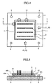
- FIG. 4 is a plan view for explaining the first half of process in a method for fabricating a flat, light-emitting display panel as embodiment 1 according to the invention.
- FIG. 5 is a cross sectional view taken along lines V-V of FIG. 4.
- FIG. 6 is a plan view for explaining the second half of process in the method for fabricating a flat, light-emitting display panel as embodiment 1 according to the invention.
- FIG. 7 is a cross sectional view taken along lines VII-VII of FIG. 6.
- FIG. 8 is an enlarged cross sectional view for explaining a process of application of the frit seal to the pin electrode in the method for fabricating a flat, light-emitting display panel as embodiment 1 according to the invention.
- components of the embodiment 1, which are common to the components shown in FIG. 1 to FIG. 3 disclosed in the previous application, are denoted by the same reference numerals and further description will be omitted.
- a reference numeral 6 denotes a plurality of pin electrodes mounted on electrodes of the front panel 1.
- a reference numeral 7 denotes a slit-shaped through hole formed at the rear panel 2 and allowing the penetration of the pin electrodes 6.
- a reference numeral 8 denotes a locating purpose base plate (base plate) for setting a relative location between the front panel 1 and the rear panel 2.
- a reference numeral 9 denotes screw holes formed in the four corners of the base plate 8.
- a reference numeral 10 denotes a location purpose pin projected from a required position of the base plate 8. The location purpose pin 10 is a tier-pin.
- a diameter of an upper section 10a of the pin 10 is set to be larger than that of a lower section 10b of the pin 10 by one-half of difference in length between one edge of the front panel 1 and one edge of the rear panel 2.
- the upper section 10a comes in contact with a side section of the rear panel 2 and the lower section 10b comes in contact with a side section of the front panel 1.
- the stacked panels 1 and 2 are placed on the base plate 8.
- the pin electrode 6 of the front panel 1 is passed through the slit-shaped through hole 7 of the rear panel 2 as shown in FIG. 4 and FIG. 5.
- the side of the front panel 1 is pressed against the lower section 10b of the location purpose pin 10 due to a force indicated by arrow F1.
- the side of the rear panel 2 is pressed against the upper section 10a of the location purpose pin 10 due to a force indicated by arrow F2.
- the force indicated by F1 and F2 may be produced by a manual operation, or by using a biasing force of spring and so on, or by using a tightening force of screws, or by using a pneumatic pressure.
- the rear panel 2 is pressed down by using a press plate (flat plate) 11 as shown in FIG. 6 and FIG. 7.
- the press plate 11 is provided with a slit-shaped hole 12 formed at a position corresponding to the pin electrode 6 as in the case of the slit-shaped through hole 7 of the rear panel 2, the pin electrode 6 is passed through the slit-shaped hole 12.
- the press plate 11 fixes provisionally the base plate 8 using a screw 13 screwed in the screw hole 9.
- the screws 9 are fixed at the screw holes 9 which are formed at least at four corners of the base plate 8.
- the screws 9 may be fixed at eight positions, for example, formed along the peripheries of the press plate 11, if necessary.
- both of the panels 1 and 2 are pressed across the whole of the panels due to the fix of the press plate 11 and the base plate 8.
- the frit seal 4 is applied to a base section of the pin electrode 6 within the slit-shaped through hole 7 of the rear panel 2 using a dispenser 14 as shown in FIG. 8.
- the pin electrode 6 is coated with the frit seal 4 through the slit-shaped through hole 7.
- the press plate 11 must have a thickness to a certain extent in order to prevent it from deforming. When the press plate 11 is too thick, it is difficult to apply the frit seal 4 to the pin electrode 6. It is preferable that the press plate 11 is approximately 2mm to 3mm thick, and the invention is limited to this range.
- a tapered section 12a is formed at a peripheral section of the slit-shaped hole 12 formed at the press plate 11 as shown in FIG. 8.
- the frit seal 4 is dried, and then the both panels 1 and 2 are removed from a jig including the base plate 8 and the press plate 11.
- the pin electrode is fixed provisionally using the dried frit seal 4.
- the both panels 1 and 2 intend to deform due to a warping force of the panels exerted on the pin electrode 6 fixed provisionally as a fulcrum.
- both of the panels 1 and 2 are hardly deformed and plane in parallel with the base plate 8 because the pin electrodes 6 are arranged in close to the ends of the panels.
- the frit seal 4 is applied to the side faces of the respective panels 1 and 2 using the dispenser 14.
- both of the panels 1 and 2 are preferably fixed in a state of the both being plane, a gap between ends of the panels is reduced to a slight of 0.04mm or less. Therefore, the amount of spread of the frit seal 4 into the gap becomes very little.
- the pipe-shaped, tipped section is fixed using the frit seal 4.
- the frit seal 4 is then burned on condition that the weights (not shown) are placed on both of the panels 1 and 2 to seal the margin of the both panels 1 and 2.
- Each of the weights has a hole through which the pin electrode 6 and the pipe-shaped, tipped section (not shown) are passed. The hole prevents the weights from pressing both of the panels 1 and 2 and allows a part other than the pin electrode 6 and so on to be pressed uniformly. Unless the pressure is exerted uniformly on both of the panels 1 and 2, the frit seal 4 softened on burning is spread into the cell.
- both of the panels 1 and 2 are fixed provisionally on condition that the panels 1 and 2 are kept uniformly in contact with one another using the press plate 11. In this way, it is possible to prevent a gap formed between both of the panels 1 and 2 due to their warping and to prevent the frit seal 4 from spreading into the gap between both of the panels 1 and 2.
- FIG. 9 is a plan view for explaining a process in the method for fabricating a flat, light-emitting display panel as embodiment 2 according to the invention.
- FIG. 10 is a cross sectional view taken along lines X-X of FIG. 9. Components of the embodiment 2 common to the components of the embodiment 1 are denoted by the same reference numerals and further description will be omitted.
- the embodiment 2 is characterized in that a plural of coil springs (biasing means) 15 are disposed between the rear panel 2 and the press plate 11 at appropriate intervals.
- Each of the coil springs 15 works in a direction of increasing a distance between the rear panel 2 and the press plate 11. Since the distance is increased due to a biasing force of the coil spring 15, the front panel 1 and the rear panel 2 can be kept uniformly in contact with one another due to a stress of the press plate 11 exerted on the rear panel 2.
- biasing means is not limited to forms of the coil spring 15.
- Elastic body such as leaf springs, air springs, or rubber bush is available, and is used as appropriate in consideration of required contact characteristics or cost.
- the frit seal is applied to the pin electrode 6 and then the side of the panel.
- the application of the frit seal is performed in inverse order. That is, with the embodiment 3, the frit seal is applied to the side of the panel on condition that the whole of the panels 1 and 2 is pressed uniformly, and is dried to fix provisionally the both panels 1 and 2. The frit seal is then applied to the pin electrode 6 and is burned.
- the front panel 1 and the rear panel 2 are fixed provisionally on condition that the whole of the panels 1 and 2 is pressed uniformly as in the case of the embodiment 1 or 2. In this way, it is possible to prevent a gap formed between both of the panels 1 and 2 due to their warping and to prevent the frit seal 4 from spreading into the gap between both of the panels 1 and 2.
- the press plate 8 is used in pressing uniformly the whole of the panels 1 and 2, as in the case of the embodiment 1 or 2.
- a weight 16 may be used in pressing uniformly them. That is, a recess 16a, which avoids coming in contact with the pin electrode 6, is formed in a lower face of the weight 16.
- the weight 16 is placed on the rear panel 2 stacked on the front panel 1. In such a state, the frit seal is applied to the side of the both panels 1 and 2.
- the weight 16 is heavier than the press plate 11 in the embodiment 1 or 2, it is possible to reduce the gap between the both panels 1 and 2 to the limit and to prevent spread of the frit seal 4 with reliability.
- the press plate 11 since the press plate 11 has no use for pressing the panels, it is possible to reduce a component count and to simplify a fabricating process.
- the weight 16 pressing uniformly the both panels 1 and 2 may be preferably replaced by, for example, spring members, compressed air and so on.
- the embodiment 4 is characterized in that a frit seal, which is applied to the side of the panels, has flowability less than a frit seal applied to the pin electrodes 6. In this way, it is possible to coat the electrode with the frit seal and to reduce the spread of the frit seal into the side of the panels.
- the frit seal is a mixture of mixing PbO-B2O3 system glass powder, for example, with filler such ceramic powder. Factors such as the quality of the filler, a mixing ratio, a particle diameter and so on are changed, and it is therefore possible to control the flowability of the frit seal. Examples of the combination of various kinds of frit each having different flowability includes LS-0118 and LS-0206 prepared by Japanese Electronics and Glass Co. Ltd., for example. The temperature condition in sealing such as 430 degrees centigrade for ten minutes or 450 degrees centigrade for fifteen minutes is recommended. That is, when two kinds of the frit seal is burned on the same temperature and the same period, the LS-0206 has flowability less than the LS-0118.
- the LS-0118 having high flowability relative to the other is used to be applied to the pin electrode 6, and the LS-0206 having low flowability relative to the other is used to be applied to the side of the panels.
- the frit seal is burned at the temperature of 445 degrees centigrade for fifteen minutes. In this way, it is possible to coat perfectly the pin electrode 6 with the frit seal having high flowability, and to prevent entirely the spread of the frit seal having low flowability into the side of the panels.
- the frit seal of LS-0118 is replaced by DT-430 prepared by Iwaki glass Co. Ltd., having the property as in the case of the two kinds of frit seal above.
- a method for fabricating a flat, light-emitting display panel according to the invention is adequate to fabricate a display panel having no gap between a plurality of panels.
- the fabricated display panel is adequate for image on the large-screen comprised of panels tiled.
Landscapes
- Engineering & Computer Science (AREA)
- Manufacturing & Machinery (AREA)
- Manufacture Of Electron Tubes, Discharge Lamp Vessels, Lead-In Wires, And The Like (AREA)
- Gas-Filled Discharge Tubes (AREA)
Abstract
A method for fabricating a flat, light-emitting display panel
includes the steps of applying frit seal to the pin electrodes in a state
of pressing the rear panel against the front panel to keep them in contact
with one another using a flat plate having an opening formed at a position
corresponding to each of the pin electrodes; drying the frit seal to fix
provisionally the rear panel to the front panel; detaching the flat plate
from the both panels; applying frit seal to an end of the front panel and
a side face of the rear panel; and burning the whole of components. The
sequence of the application of the frit seal to the pin electrode and the
application of the frit seal to the end of the front panel and the side
face of the rear panel may be altered. The frit seal having flowability
less than the frit seal applied to the pin electrode is is applied to the
end of the front panel and the side face of the rear panel.
Description
- The invention relates to a method for fabricating a flat, light-emitting display panel having electrodes extended from a rear panel and sealing the margin of panels with a fritted glass.
- A large-screen monitor grows in demand as an information-oriented society moves forward in recent years. Generally, it is difficult in view of technical reason or cost-reduction measure that the large-screen monitor is comprised of only one display device (hereafter, referred as a panel). Therefore, plural panels are tiled to constitute the conventional large-screen monitor.
- In the case, when no-displayed area arranged at ends of each panel is large, seams defined between the adjacent panels become prominent. As a result, imagery quality of the whole of the large-screen is reduced. Therefore, it is desirable that a flat, light-emitting display panel, which has small, no-displayed area at each panel and displays a high quality of image on the large-screen, is developed.
- The applicants previously propose a structure of the flat, light-emitting display panel formed from a matrix of the plural panels to fit such a need.
- FIG. 1 is a cross sectional view of a side-seal structure of the flat, light-emitting display panel (hereafter, referred as a display panel) disclosed in the previous, co-pending application. In the drawing, a
reference numeral 1 denotes a transparent, front panel. Areference numeral 2 denotes a rear panel, which is arranged in parallel to thefront panel 1 and having a plurality ofrecesses 2a. Eachrecess 2a is defined as a discharging space for a display cell. An electrical insulating glass layer (not shown) is formed at a bottom face and an inner wall of eachrecess 2a of therear panel 2. Afluorescent substance 3 is applied on the electrical insulating glass layer. A pin electrode (not shown) penetrating therear panel 2 is arranged within thefront panel 1. A pair of cell-type electrodes (not shown) are arranged at every area of thefront panel 1 facing each of therecesses 2a of therear panel 2. - With such a constructed display panel, in order to reduce the no-displayed area in ends of display panel, the pin electrode (not shown) connecting with the electrode arranged at the
front panel 1 is extended from the rear panel. The size of thefront panel 1 is set to a value larger than that of therear panel 2. Afrit seal 4 is applied to an extended area 1a of thefront panel 1 that extends off therear panel 2 and to aside face 2b of therear panel 2 and burned the whole of components. As a result, the margin of thefront panel 1 and therear panel 2 is sealed. - Next, a method for fabricating a display panel will be explained in order of undergoing process.
- A transparent electrode (not shown) including a discharging gap is formed at the
front panel 1 using an ITO (indium-tinned oxide) or a Nesa (tinned oxide), for example. - Electric terminals are formed at one end of the transparent electrode (not shown) formed in the
previous step 1 by a screen printing method using conductive materials such as an Ag or silver and so on. - Electrical insulating glass layers (not shown) are formed at the whole of the
front panel 1 except for the electric terminals (not shown) formed in thestep 2. - Pin electrodes (not shown) are projected in the electric terminals (not shown), respectively.
- A MgO film is formed on the electrical insulating glass layer (not shown) formed in the
previous step 3 to finish all processes regarding thefront panel 1. -
Recesses 2a, which are defined as a through-hole for passing through the pin electrode (not shown) and functioned as a discharging space for a display cell, are formed at therear panel 2 using a sandblasting method and so on. - Fluorescent substance (R: red, G: green, B: blue) 3 is applied to the bottom face and the inner wall of the
recess 2a formed in theprevious step 6 using the screen printing method and so on to finish all processes regarding therear panel 2. - Each of the pin electrodes (not shown) projected at the
front panel 1 is fitted into each of the through-hole (not shown) of therear panel 2. Therear panel 2 is stacked to thefront panel 1 so that thefluorescent substance 3 faces thefront panel 1. - Ends of the
front panel 1 and those of therear panel 2 having no pin electrodes are stacked and fixed using a spring-loaded clip (not shown) . - A frit seal is applied to the pin electrode (not shown) using a dispenser (not shown).
- After the
frit seal 4 applied in theprevious step 10 is dried, the spring-quipped clip (not shown) is removed. Thefrit seal 4 is applied to a pipe-shaped, tipped section (not shown) and an outer periphery of the panel, that is, the extended area 1a of thefront panel 1 and theside face 2b of therear panel 2 using the dispenser (not shown). - Weights (not shown) is placed at a part other than the pipe-shaped, tipped section (not shown) and the pin electrode (not shown) and the
frit seal 4 is then burned. Air is exhausted from a space between the panels and discharge gas is filled and sealed in the space. - The MgO adhered to the pin electrode (not shown) is removed using a sandblasting method and so on. In this way, a display panel is obtained.
- When plural display panels, which are fabricated by the processes as described above and disclosed in the previous application, are arranged, lighted and displayed, there may be case where a display gap is formed between adjacent panels.
- The present inventors investigated adequately the cause of gap in the display panel and found that a frit seal, which is formed at the extended area 1a of the
front panel 1 and theside face 2b of therear panel 2, is spread into the display cell. Namely, when thefluorescent substance 3 applied to therear panel 2 or an area of thefront panel 1 corresponding to thefluorescent substance 3 is covered with the frit seal spread into the display cell, light is not emitted or cut off from the covered section. Therefore, it results in no-emitting area or no-displayed area being increased at the ends of the display panel. The no-emitting area is considered to seem like a gap between adjacent panels. - A gap between the front and
rear panels frit seal 4 is applied to the extended area 1a of thefront panel 1 and theside face 2b of therear panel 2 is considered to become a cause of spread of the frit seal. In thestep 11, the spring-loaded clip (not shown) is removed and a distance of a gap between thefront panel 1 and therear panel 2 is measured using a gap-measurement gage (not shown) before the gap is sealed with the frit seal. As a result, a gap of approximately 0.15mm was found. When a large-sized gap is formed at the gap, thefrit seal 4 is applied thereto to result in thefrit seal 4 in a large amount being inserted into the gap. Thefrit seal 4 is burned in thestep 12 to result in a softenedfrit seal 4 in a large amount being inserted into the cell. - Such a gap is formed due to warping occurred in the
front panel 1 and therear panel 2. The electrical insulating glass layer (not shown) in approximately 30 um thickness is formed at a surface of thefront panel 1. Therecess 2a is formed at a surface of therear panel 2. Therefore, there has a tendency to warp any panels so as to deform their surfaces (opposite surfaces) to be convex. In the state, when the ends of the both panels are cramped using fthe spring-loadedclip 5 as shown in FIG. 5 (Step 5), both central sections of thepanels recess 2a of therear panel 2 and the pin electrode are not illustrated and are omitted in FIG. 2 and FIG. 3. Next, in order to apply thefrit seal 4 to the extended area 1a of thefront panel 1 and theside face 2b of therear panel 2, the spring-loadedclip 5 is removed. At this time, since the both panels intend to return to their original state, the gap is formed between the ends of the both panels as shown in FIG. 2. - Furthermore, the following other factors are considered to become a cause of the spread of the frit seal. That is, the
frit seal 4 is softened at the side of thefront panel 1 and therear panel 2 on burning to pass through a micro-gap between the front andrear panels frit seal 4 must be set to become a small value on softening. Therefore, we have learned that thefrit seal 4 must be burned on condition that the burning is performed at a low temperature or for a short time. - However, when the
frit seal 4 is burned on such a condition, reduction of the spread of thefrit seal 4 into the cell can occur. When a voltage is applied to the displaypanel, there are malfunctions that discharge occurs abnormally at the pin electrodes. There is a reason: when thefrit seal 4 is burned on the condition above, thefrit seal 4 having a low flowability can not flow adequately into the pin electrode. The pin electrode is coated inadequately with thefrit seal 4 and the insulating properties are reduced. As a result, the discharge occurs abnormally when the voltage is applied to the display panel. - On the other hand, in order to coat perfectly the pin electrode, it is necessary to burn the
frit seal 4 at a high temperature or for a long time. In such a case, there is a malfunction that the softenedfrit seal 4 applied to the ends of the panel is spread into the cell. That is, the coating of the pin electrode and the spreading of the frit seal applied to the ends of the panel are mutually contradictory and it is difficult to maintain compatibility between both sides. - The invention was made to solve the foregoing problems. Accordingly, it is an object of the invention to provide a method for fabricating a flat, light-emitting display panel that a pin electrode can be coated perfectly with a frit seal and that reduction of the spread of the frit seal into a cell can occur.
- In order to achieve the object of the invention, we provide a method for fabricating a flat, light-emitting display panel including a transparent, front panel, a rear panel arranged in parallel to the front panel and having a plurality of recesses, each recess being defined as a discharging space for a display cell, a pin electrode projected inwardly in a state of penetrating the rear panel, and a pair of cell-type electrodes, which works at the presence of voltage from the pin electrodes, arranged at every area of the front panel facing each of the recesses of the rear panel, wherein the method comprises the steps of: applying frit seal to the pin electrodes in a state of pressing the rear panel against the front panel to keep them in contact with one another using a flat plate having an opening formed at a position corresponding to each of the pin electrodes; drying the frit seal to fix provisionally the rear panel to the front panel; detaching the flat plate from the both panels; applying frit seal to an end of the front panel and a side face of the rear panel; and burning the whole of components. In this way, both of the panels are fixed provisionally on condition that the panels are kept uniformly in contact with one another using the flat plate. In this way, it is possible to prevent a gap formed between both of the panels due to their warping and to prevent the frit seal from spreading into the gap between both of the panels. Moreover, it is unnecessary to vary conditions for burning the frit seal. The frit seal is therefore burned on condition that the
pin electrodes 6 can be coated adequately. - With the above arrangement, the method may comprise the steps of: placing both of the front panel and the rear panel stacked to the front panel on a base plate having a flat face; and securing the flat plate to the base plate by screws. In this way, the front panel and the rear panel are sandwiched between the flat plate and the base plate to keep the both panels in contact with one another. It is therefore possible to reliably prevent the spread of the frit seal into the gap between the both panels on application of the frit seal and on burning.
- With the above arrangement, the method may comprise the steps of: placing both of the front panel and the rear panel stacked to the front panel on a base plate having a flat face; and securing the flat plate to the base plate by screws through a plurality of biasing means. In this way, the front panel and the rear panel are sandwiched between the flat plate and the base plate to keep the both panels in contact with one another. It is therefore possible to reliably prevent the spread of the frit seal into the gap between the both panels on application of the frit seal and on burning.
- With the above arrangement, the frit seal, which is applied to the end of the front panel and the side face of the rear panel, may have flowability less than the frit seal applied to the pin electrodes. In this way, it is possible to reduce the amount of the frit seal, which spreads from the margins of the both panels into the gap, to the minimum level.
- We provide a method for fabricating a flat, light-emitting display panel including a transparent, front panel, a rear panel arranged in parallel to the front panel and having a plurality of recesses, each recess being defined as a discharging space for a display cell, a pin electrode projected inwardly in a state of penetrating the rear panel, and a pair of cell-type electrodes, which works at the presence of voltage from the pin electrodes, arranged at every area of the front panel facing each of the recesses of the rear panel, wherein the method comprises the steps of: applying frit seal to an end of the front panel and a side face of the rear panel in a state of pressing the rear panel against the front panel to keep them in contact with one another using a flat plate having an opening formed at a position corresponding to each of the pin electrodes; drying the frit seal to fix provisionally the rear panel to the front panel; detaching the flat plate from the both panels; applying frit seal to the pin electrodes; and burning the whole of components. In this way, both of the panels are fixed provisionally on condition that the panels are kept uniformly in contact with one another using the flat plate. In this way, it is possible to prevent a gap formed between both of the panels due to their warping and to prevent the frit seal from spreading in to the gap between both of the panels. Moreover, it is unnecessary to vary conditions for burning the frit seal. The frit seal is therefore burned on condition that the
pin electrodes 6 can be coated adequately. - With the above arrangement, the method may comprise the steps of: placing both of the front panel and the rear panel stacked to the front panel on a base plate having a flat face; and securing the flat plate to the base plate by screws. In this way, the front panel and the rear panel are sandwiched between the flat plate and the base plate to keep the both panels in contact with one another. It is therefore possible to reliably prevent the spread of the frit seal into the gap between the both panels on application of the frit seal and on burning.
- With the above arrangement, the method may comprise the steps of: placing both of the front panel and the rear panel stacked to the front panel on a base plate having a flat face; and securing the flat plate to the base plate by screws through a plurality of biasing means. In this way, the front panel and the rear panel are sandwiched between the flat plate and the base plate to keep the both panels in contact with one another. It is therefore possible to reliably prevent the spread of the frit seal into the gap between the both panels on application of the frit seal and on burning.
- With the above arrangement, the frit seal, which is applied to the end of the front panel and the side face of the rear panel, may have flowability less than the frit seal applied to the pin electrodes. In this way, it is possible to reduce the amount of the frit seal, which spreads from the margins of the both panels into the gap, to the minimum level.
-
- FIG. 1 is a cross sectional view of a side-seal structure of the flat, light-emitting display panel disclosed in the previous application.
- FIG. 2 is a cross sectional view of a state of warping occurred in the front and rear panels.
- FIG. 3 is a cross sectional view for explaining a method of correcting the warping occurred in the front and rear panels, shown in FIG. 2.
- FIG. 4 is a plan view for explaining the first half of process in
a method for fabricating a flat, light-emitting display panel as
embodiment 1 according to the invention. - FIG. 5 is a cross sectional view taken along lines V-V of FIG. 4.
- FIG. 6 is a plan view for explaining the second half of process
in the method for fabricating a flat, light-emitting display panel as
embodiment 1 according to the invention. - FIG. 7 is a cross sectional view taken along lines VII-VII of FIG. 6.
- FIG. 8 is an enlarged cross sectional view for explaining a process
of application of the frit seal to the pin electrode in the method for
fabricating a flat, light-emitting display panel as
embodiment 1 according to the invention. - FIG. 9 is a plan view for explaining a process in the method for
fabricating a flat, light-emitting display panel as
embodiment 2 according to the invention. - FIG. 10 is a cross sectional view taken along lines X-X of FIG. 9.
- FIG. 11 is an enlarged cross sectional view for explaining a process
in the method for fabricating a flat, light-emitting display panel as
embodiment 3 according to the invention. -
- To explain the invention more in detail, the best modes of carrying out the invention will be described with reference to the accompanying drawings.
- FIG. 4 is a plan view for explaining the first half of process in a method for fabricating a flat, light-emitting display panel as
embodiment 1 according to the invention. FIG. 5 is a cross sectional view taken along lines V-V of FIG. 4. FIG. 6 is a plan view for explaining the second half of process in the method for fabricating a flat, light-emitting display panel asembodiment 1 according to the invention. FIG. 7 is a cross sectional view taken along lines VII-VII of FIG. 6. FIG. 8 is an enlarged cross sectional view for explaining a process of application of the frit seal to the pin electrode in the method for fabricating a flat, light-emitting display panel asembodiment 1 according to the invention. Moreover, components of theembodiment 1, which are common to the components shown in FIG. 1 to FIG. 3 disclosed in the previous application, are denoted by the same reference numerals and further description will be omitted. - In the drawing, a
reference numeral 6 denotes a plurality of pin electrodes mounted on electrodes of thefront panel 1. Areference numeral 7 denotes a slit-shaped through hole formed at therear panel 2 and allowing the penetration of thepin electrodes 6. Areference numeral 8 denotes a locating purpose base plate (base plate) for setting a relative location between thefront panel 1 and therear panel 2. Areference numeral 9 denotes screw holes formed in the four corners of thebase plate 8. Areference numeral 10 denotes a location purpose pin projected from a required position of thebase plate 8. Thelocation purpose pin 10 is a tier-pin. A diameter of anupper section 10a of thepin 10 is set to be larger than that of alower section 10b of thepin 10 by one-half of difference in length between one edge of thefront panel 1 and one edge of therear panel 2. Theupper section 10a comes in contact with a side section of therear panel 2 and thelower section 10b comes in contact with a side section of thefront panel 1. - Next, a method for fabricating a display panel as the
embodiment 1 will be explained in order of undergoing process. - First, the
stacked panels base plate 8. At this time, thepin electrode 6 of thefront panel 1 is passed through the slit-shaped throughhole 7 of therear panel 2 as shown in FIG. 4 and FIG. 5. The side of thefront panel 1 is pressed against thelower section 10b of thelocation purpose pin 10 due to a force indicated by arrow F1. At the same time, the side of therear panel 2 is pressed against theupper section 10a of thelocation purpose pin 10 due to a force indicated by arrow F2. In this way, both of thefront panel 1 and therear panel 2 are centered. The force indicated by F1 and F2 may be produced by a manual operation, or by using a biasing force of spring and so on, or by using a tightening force of screws, or by using a pneumatic pressure. - Next, the
rear panel 2 is pressed down by using a press plate (flat plate) 11 as shown in FIG. 6 and FIG. 7. Here, since thepress plate 11 is provided with a slit-shapedhole 12 formed at a position corresponding to thepin electrode 6 as in the case of the slit-shaped throughhole 7 of therear panel 2, thepin electrode 6 is passed through the slit-shapedhole 12. Next, thepress plate 11 fixes provisionally thebase plate 8 using ascrew 13 screwed in thescrew hole 9. At this time, since thefront panel 1 and therear panel 2 are pressed across the whole of the panels, thepanels screws 9 are fixed at the screw holes 9 which are formed at least at four corners of thebase plate 8. Alternatively, as shown in FIG. 6, thescrews 9 may be fixed at eight positions, for example, formed along the peripheries of thepress plate 11, if necessary. - Next, both of the
panels press plate 11 and thebase plate 8. In such a condition, thefrit seal 4 is applied to a base section of thepin electrode 6 within the slit-shaped throughhole 7 of therear panel 2 using adispenser 14 as shown in FIG. 8. Thepin electrode 6 is coated with thefrit seal 4 through the slit-shaped throughhole 7. Moreover, thepress plate 11 must have a thickness to a certain extent in order to prevent it from deforming. When thepress plate 11 is too thick, it is difficult to apply thefrit seal 4 to thepin electrode 6. It is preferable that thepress plate 11 is approximately 2mm to 3mm thick, and the invention is limited to this range. In order to facilitate the application of thefrit seal 4, atapered section 12a is formed at a peripheral section of the slit-shapedhole 12 formed at thepress plate 11 as shown in FIG. 8. - Next, the
frit seal 4 is dried, and then the bothpanels base plate 8 and thepress plate 11. In such a condition, the pin electrode is fixed provisionally using the driedfrit seal 4. The bothpanels pin electrode 6 fixed provisionally as a fulcrum. However, both of thepanels base plate 8 because thepin electrodes 6 are arranged in close to the ends of the panels. - In such a condition, the
frit seal 4 is applied to the side faces of therespective panels dispenser 14. At this time, since both of thepanels frit seal 4 into the gap becomes very little. - Next, the pipe-shaped, tipped section is fixed using the
frit seal 4. Thefrit seal 4 is then burned on condition that the weights (not shown) are placed on both of thepanels panels pin electrode 6 and the pipe-shaped, tipped section (not shown) are passed. The hole prevents the weights from pressing both of thepanels pin electrode 6 and so on to be pressed uniformly. Unless the pressure is exerted uniformly on both of thepanels frit seal 4 softened on burning is spread into the cell. - As described above, according to the
embodiment 1, both of thepanels panels press plate 11. In this way, it is possible to prevent a gap formed between both of thepanels frit seal 4 from spreading into the gap between both of thepanels - As described above, with the
embodiment 1, it is unnecessary to vary conditions for burning the frit seal. The frit seal is therefore burned on condition that thepin electrodes 6 can be coated adequately. - FIG. 9 is a plan view for explaining a process in the method for fabricating a flat, light-emitting display panel as
embodiment 2 according to the invention. FIG. 10 is a cross sectional view taken along lines X-X of FIG. 9. Components of theembodiment 2 common to the components of theembodiment 1 are denoted by the same reference numerals and further description will be omitted. - The
embodiment 2 is characterized in that a plural of coil springs (biasing means) 15 are disposed between therear panel 2 and thepress plate 11 at appropriate intervals. Each of the coil springs 15 works in a direction of increasing a distance between therear panel 2 and thepress plate 11. Since the distance is increased due to a biasing force of thecoil spring 15, thefront panel 1 and therear panel 2 can be kept uniformly in contact with one another due to a stress of thepress plate 11 exerted on therear panel 2. - Moreover, with the
embodiment 2, recesses allowing a part of thecoil spring 15 defined as the biasing means to be inserted are formed in the lower face of thepress plate 11. The biasing means is not limited to forms of thecoil spring 15. Elastic body such as leaf springs, air springs, or rubber bush is available, and is used as appropriate in consideration of required contact characteristics or cost. - With the
embodiment pin electrode 6 and then the side of the panel. With theembodiment 3, the application of the frit seal is performed in inverse order. That is, with theembodiment 3, the frit seal is applied to the side of the panel on condition that the whole of thepanels panels pin electrode 6 and is burned. - According to the
embodiment 3, thefront panel 1 and therear panel 2 are fixed provisionally on condition that the whole of thepanels embodiment panels frit seal 4 from spreading into the gap between both of thepanels - Moreover, with the
embodiment 3, thepress plate 8 is used in pressing uniformly the whole of thepanels embodiment weight 16 may be used in pressing uniformly them. That is, arecess 16a, which avoids coming in contact with thepin electrode 6, is formed in a lower face of theweight 16. Theweight 16 is placed on therear panel 2 stacked on thefront panel 1. In such a state, the frit seal is applied to the side of the bothpanels weight 16 is heavier than thepress plate 11 in theembodiment panels frit seal 4 with reliability. With theembodiment 3 of using theweight 16, since thepress plate 11 has no use for pressing the panels, it is possible to reduce a component count and to simplify a fabricating process. - Moreover, the
weight 16 pressing uniformly the bothpanels - The
embodiment 4 is characterized in that a frit seal, which is applied to the side of the panels, has flowability less than a frit seal applied to thepin electrodes 6. In this way, it is possible to coat the electrode with the frit seal and to reduce the spread of the frit seal into the side of the panels. - The frit seal is a mixture of mixing PbO-B2O3 system glass powder, for example, with filler such ceramic powder. Factors such as the quality of the filler, a mixing ratio, a particle diameter and so on are changed, and it is therefore possible to control the flowability of the frit seal. Examples of the combination of various kinds of frit each having different flowability includes LS-0118 and LS-0206 prepared by Japanese Electronics and Glass Co. Ltd., for example. The temperature condition in sealing such as 430 degrees centigrade for ten minutes or 450 degrees centigrade for fifteen minutes is recommended. That is, when two kinds of the frit seal is burned on the same temperature and the same period, the LS-0206 has flowability less than the LS-0118. Therefore, the LS-0118 having high flowability relative to the other is used to be applied to the
pin electrode 6, and the LS-0206 having low flowability relative to the other is used to be applied to the side of the panels. The frit seal is burned at the temperature of 445 degrees centigrade for fifteen minutes. In this way, it is possible to coat perfectly thepin electrode 6 with the frit seal having high flowability, and to prevent entirely the spread of the frit seal having low flowability into the side of the panels. Moreover, the frit seal of LS-0118 is replaced by DT-430 prepared by Iwaki glass Co. Ltd., having the property as in the case of the two kinds of frit seal above. - As described above, according to the
embodiment 4, since the various kinds of the frit seal are used depending on places to which they are applied, it is possible to improve image quality on request to the display panel. - As described above, a method for fabricating a flat, light-emitting display panel according to the invention is adequate to fabricate a display panel having no gap between a plurality of panels. The fabricated display panel is adequate for image on the large-screen comprised of panels tiled.
Claims (8)
- A method for fabricating a flat, light-emitting display panel including a transparent, front panel, a rear panel arranged in parallel to the front panel and having a plurality of recesses, each recess being defined as a discharging space for a display cell, a pin electrode projected inwardly in a state of penetrating the rear panel, and a pair of cell-type electrodes, which works at the presence of voltage from the pin electrodes, arranged at every area of the front panel facing each of the recesses of the rear panel,
wherein the method comprises the steps of:applying frit seal to the pin electrodes in a state of pressing the rear panel against the front panel to keep them in contact with one another using a flatplate having an opening formed at a position corresponding to each of the pin electrodes;drying the frit seal to fix provisionally the rear panel to the front panel;detaching the flat plate from the both panels;applying frit seal to an end of the front panel and a side face of the rear panel; andburning the whole of components. - A method for fabricating a flat, light-emitting display panel according to Claim 1, comprising the steps of:placing both of the front panel and the rear panel stacked to the front panel on a base plate having a flat face; andsecuring the flat plate to the base plate by screws.
- A method for fabricating a flat, light-emitting display panel according to Claim 1, comprising the steps of:placing both of the front panel and the rear panel stacked to the front panel on a base plate having a flat face; andsecuring the flat plate to the base plate by screws through a plurality of biasing means.
- A method for fabricating a flat, light-emitting display panel according to Claim 1, wherein the frit seal, which is applied to the end of the front panel and the side face of the rear panel, has flowability less than the frit seal applied to the pin electrodes.
- A method for fabricating a flat, light-emitting display panel including a transparent, front panel, a rear panel arranged in parallel to the front panel and having a plurality of recesses, each recess being defined as a discharging space for a display cell, a pin electrode projected inwardly in a state of penetrating the rear panel, and a pair of cell-type electrodes, which works at the presence of voltage from the pin electrodes, arranged at every area of the front panel facing each of the recesses of the rear panel,
wherein the method comprises the steps of:applying frit seal to an end of the front panel and a side face of the rear panel in a state of pressing the rear panel against the front panel to keep them in contact with one another using a flat plate having an opening formed at a position corresponding to each of the pin electrodes;drying the frit seal to fix provisionally the rear panel to the front panel;detaching the flat plate from the both panels;applying frit seal to the pin electrodes; andburning the whole of components. - A method for fabricating a flat, light-emitting display panel according to Claim 5, comprising the steps of:placing both of the front panel and the rear panel stacked to the front panel on a base plate having a flat face; andsecuring the flat plate to the base plate by screws.
- A method for fabricating a flat, light-emitting display panel according to Claim 5, comprising the steps of:placing both of the front panel and the rear panel stacked to the front panel on a base plate having a flat face; andsecuring the flat plate to the base plate by screws through a plurality of biasing means.
- A method for fabricating a flat, light-emitting display panel according to Claim 5, wherein the frit seal, which is applied to the end of the front panel and the side face of the rear panel, has flowability less than the frit seal applied to the pin electrodes.
Applications Claiming Priority (1)
| Application Number | Priority Date | Filing Date | Title |
|---|---|---|---|
| PCT/JP2000/005289 WO2002013223A1 (en) | 2000-08-07 | 2000-08-07 | Method of producing planar type light-emitting display panels |
Publications (2)
| Publication Number | Publication Date |
|---|---|
| EP1308981A1 true EP1308981A1 (en) | 2003-05-07 |
| EP1308981A4 EP1308981A4 (en) | 2006-02-15 |
Family
ID=11736332
Family Applications (1)
| Application Number | Title | Priority Date | Filing Date |
|---|---|---|---|
| EP00950028A Withdrawn EP1308981A4 (en) | 2000-08-07 | 2000-08-07 | METHOD FOR MANUFACTURING FLAT TYPE ACTIVE DISPLAYS |
Country Status (4)
| Country | Link |
|---|---|
| EP (1) | EP1308981A4 (en) |
| JP (1) | JP3759727B2 (en) |
| KR (1) | KR100445954B1 (en) |
| WO (1) | WO2002013223A1 (en) |
Families Citing this family (1)
| Publication number | Priority date | Publication date | Assignee | Title |
|---|---|---|---|---|
| WO2008149804A1 (en) * | 2007-06-08 | 2008-12-11 | Ulvac, Inc. | Method and apparatus for manufacturing sealing panel and method and apparatus for manufacturing plasma display panel |
Family Cites Families (4)
| Publication number | Priority date | Publication date | Assignee | Title |
|---|---|---|---|---|
| JPH07307131A (en) * | 1994-05-13 | 1995-11-21 | Canon Inc | Image forming apparatus manufacturing method |
| US6323596B1 (en) * | 1997-03-31 | 2001-11-27 | Mitsubishi Denki Kabushiki Kaisha | Planar display panel and panel manufacturing method |
| JP3442294B2 (en) * | 1998-09-29 | 2003-09-02 | 三菱電機株式会社 | Flat panel |
| JP2000133134A (en) * | 1998-10-22 | 2000-05-12 | Sony Corp | Frit sealing method for flat display device, jig for frit sealing and alignment device |
-
2000
- 2000-08-07 KR KR10-2002-7004440A patent/KR100445954B1/en not_active Expired - Fee Related
- 2000-08-07 JP JP2002518490A patent/JP3759727B2/en not_active Expired - Fee Related
- 2000-08-07 EP EP00950028A patent/EP1308981A4/en not_active Withdrawn
- 2000-08-07 WO PCT/JP2000/005289 patent/WO2002013223A1/en not_active Ceased
Non-Patent Citations (2)
| Title |
|---|
| No further relevant documents disclosed * |
| See also references of WO0213223A1 * |
Also Published As
| Publication number | Publication date |
|---|---|
| WO2002013223A1 (en) | 2002-02-14 |
| JP3759727B2 (en) | 2006-03-29 |
| KR100445954B1 (en) | 2004-08-25 |
| KR20020048950A (en) | 2002-06-24 |
| EP1308981A4 (en) | 2006-02-15 |
Similar Documents
| Publication | Publication Date | Title |
|---|---|---|
| US6677704B2 (en) | AC-type gas discharge display with elliptical discharge tube | |
| US20020111102A1 (en) | Plasma display panel having a dielectric layer of a reduced thickness in a sealing portion | |
| EP1308981A1 (en) | Method of producing planar type light-emitting display panels | |
| US6746294B1 (en) | Method for fabricating a flat, light-emitting display panel | |
| US6152796A (en) | Method for manufacturing an image forming apparatus | |
| US7719191B2 (en) | Plasma display panel | |
| US5581149A (en) | Display tube for light source | |
| JPWO2002013223A1 (en) | Method for manufacturing a flat-type light-emitting display panel | |
| JPH03225743A (en) | Flat rare gas discharge lamp | |
| US8008847B2 (en) | Manufacturing method of gas discharge tube, gas discharge tube, and display device | |
| JP3358385B2 (en) | Adhesive smoothing method | |
| TW470991B (en) | Manufacturing method of planar light emitting display panel | |
| JP2005085581A (en) | Field emission display | |
| US20050116613A1 (en) | Image display device | |
| JP3091158B2 (en) | Method of manufacturing gas discharge display panel | |
| KR100724638B1 (en) | Image display device | |
| KR100247415B1 (en) | Method and apparatus for aging plasma display panel | |
| KR101023140B1 (en) | Flat panel display | |
| US5257018A (en) | Display device | |
| JP2003203586A (en) | Flat display device and method of manufacturing the same | |
| JP2618106B2 (en) | Plasma display | |
| EP2423940B1 (en) | Field emission panel, liquid crystal display having the same and field emission display having the same | |
| JPS6250882A (en) | Fluorescent display unit | |
| CN1163939C (en) | Discharge display device and method for manufacturing the same | |
| KR20060064165A (en) | Plasma display panel |
Legal Events
| Date | Code | Title | Description |
|---|---|---|---|
| PUAI | Public reference made under article 153(3) epc to a published international application that has entered the european phase |
Free format text: ORIGINAL CODE: 0009012 |
|
| 17P | Request for examination filed |
Effective date: 20020405 |
|
| AK | Designated contracting states |
Designated state(s): AT BE CH CY DE DK ES FI FR GB GR IE IT LI LU MC NL PT SE |
|
| RBV | Designated contracting states (corrected) |
Designated state(s): AT BE CH DE FR GB LI |
|
| A4 | Supplementary search report drawn up and despatched |
Effective date: 20051230 |
|
| RAP1 | Party data changed (applicant data changed or rights of an application transferred) |
Owner name: MITSUBISHI DENKI KABUSHIKI KAISHA |
|
| STAA | Information on the status of an ep patent application or granted ep patent |
Free format text: STATUS: THE APPLICATION HAS BEEN WITHDRAWN |
|
| 18W | Application withdrawn |
Effective date: 20060904 |