EP1308947A2 - Optischer Kopf und Verfahrung zur seinen Herstellung - Google Patents
Optischer Kopf und Verfahrung zur seinen Herstellung Download PDFInfo
- Publication number
- EP1308947A2 EP1308947A2 EP02250683A EP02250683A EP1308947A2 EP 1308947 A2 EP1308947 A2 EP 1308947A2 EP 02250683 A EP02250683 A EP 02250683A EP 02250683 A EP02250683 A EP 02250683A EP 1308947 A2 EP1308947 A2 EP 1308947A2
- Authority
- EP
- European Patent Office
- Prior art keywords
- lens
- optical head
- optical
- plate
- lens holder
- Prior art date
- Legal status (The legal status is an assumption and is not a legal conclusion. Google has not performed a legal analysis and makes no representation as to the accuracy of the status listed.)
- Withdrawn
Links
Images



Classifications
-
- G—PHYSICS
- G11—INFORMATION STORAGE
- G11B—INFORMATION STORAGE BASED ON RELATIVE MOVEMENT BETWEEN RECORD CARRIER AND TRANSDUCER
- G11B11/00—Recording on or reproducing from the same record carrier wherein for these two operations the methods are covered by different main groups of groups G11B3/00 - G11B7/00 or by different subgroups of group G11B9/00; Record carriers therefor
- G11B11/10—Recording on or reproducing from the same record carrier wherein for these two operations the methods are covered by different main groups of groups G11B3/00 - G11B7/00 or by different subgroups of group G11B9/00; Record carriers therefor using recording by magnetic means or other means for magnetisation or demagnetisation of a record carrier, e.g. light induced spin magnetisation; Demagnetisation by thermal or stress means in the presence or not of an orienting magnetic field
- G11B11/105—Recording on or reproducing from the same record carrier wherein for these two operations the methods are covered by different main groups of groups G11B3/00 - G11B7/00 or by different subgroups of group G11B9/00; Record carriers therefor using recording by magnetic means or other means for magnetisation or demagnetisation of a record carrier, e.g. light induced spin magnetisation; Demagnetisation by thermal or stress means in the presence or not of an orienting magnetic field using a beam of light or a magnetic field for recording by change of magnetisation and a beam of light for reproducing, i.e. magneto-optical, e.g. light-induced thermomagnetic recording, spin magnetisation recording, Kerr or Faraday effect reproducing
- G11B11/10532—Heads
- G11B11/10541—Heads for reproducing
- G11B11/10543—Heads for reproducing using optical beam of radiation
-
- G—PHYSICS
- G11—INFORMATION STORAGE
- G11B—INFORMATION STORAGE BASED ON RELATIVE MOVEMENT BETWEEN RECORD CARRIER AND TRANSDUCER
- G11B11/00—Recording on or reproducing from the same record carrier wherein for these two operations the methods are covered by different main groups of groups G11B3/00 - G11B7/00 or by different subgroups of group G11B9/00; Record carriers therefor
- G11B11/10—Recording on or reproducing from the same record carrier wherein for these two operations the methods are covered by different main groups of groups G11B3/00 - G11B7/00 or by different subgroups of group G11B9/00; Record carriers therefor using recording by magnetic means or other means for magnetisation or demagnetisation of a record carrier, e.g. light induced spin magnetisation; Demagnetisation by thermal or stress means in the presence or not of an orienting magnetic field
- G11B11/105—Recording on or reproducing from the same record carrier wherein for these two operations the methods are covered by different main groups of groups G11B3/00 - G11B7/00 or by different subgroups of group G11B9/00; Record carriers therefor using recording by magnetic means or other means for magnetisation or demagnetisation of a record carrier, e.g. light induced spin magnetisation; Demagnetisation by thermal or stress means in the presence or not of an orienting magnetic field using a beam of light or a magnetic field for recording by change of magnetisation and a beam of light for reproducing, i.e. magneto-optical, e.g. light-induced thermomagnetic recording, spin magnetisation recording, Kerr or Faraday effect reproducing
- G11B11/1055—Disposition or mounting of transducers relative to record carriers
- G11B11/10552—Arrangements of transducers relative to each other, e.g. coupled heads, optical and magnetic head on the same base
- G11B11/10554—Arrangements of transducers relative to each other, e.g. coupled heads, optical and magnetic head on the same base the transducers being disposed on the same side of the carrier
-
- G—PHYSICS
- G11—INFORMATION STORAGE
- G11B—INFORMATION STORAGE BASED ON RELATIVE MOVEMENT BETWEEN RECORD CARRIER AND TRANSDUCER
- G11B7/00—Recording or reproducing by optical means, e.g. recording using a thermal beam of optical radiation by modifying optical properties or the physical structure, reproducing using an optical beam at lower power by sensing optical properties; Record carriers therefor
- G11B7/12—Heads, e.g. forming of the optical beam spot or modulation of the optical beam
- G11B7/135—Means for guiding the beam from the source to the record carrier or from the record carrier to the detector
- G11B7/1372—Lenses
- G11B7/1374—Objective lenses
-
- G—PHYSICS
- G11—INFORMATION STORAGE
- G11B—INFORMATION STORAGE BASED ON RELATIVE MOVEMENT BETWEEN RECORD CARRIER AND TRANSDUCER
- G11B7/00—Recording or reproducing by optical means, e.g. recording using a thermal beam of optical radiation by modifying optical properties or the physical structure, reproducing using an optical beam at lower power by sensing optical properties; Record carriers therefor
- G11B7/12—Heads, e.g. forming of the optical beam spot or modulation of the optical beam
- G11B7/135—Means for guiding the beam from the source to the record carrier or from the record carrier to the detector
- G11B7/1387—Means for guiding the beam from the source to the record carrier or from the record carrier to the detector using the near-field effect
-
- G—PHYSICS
- G11—INFORMATION STORAGE
- G11B—INFORMATION STORAGE BASED ON RELATIVE MOVEMENT BETWEEN RECORD CARRIER AND TRANSDUCER
- G11B7/00—Recording or reproducing by optical means, e.g. recording using a thermal beam of optical radiation by modifying optical properties or the physical structure, reproducing using an optical beam at lower power by sensing optical properties; Record carriers therefor
- G11B7/12—Heads, e.g. forming of the optical beam spot or modulation of the optical beam
- G11B7/135—Means for guiding the beam from the source to the record carrier or from the record carrier to the detector
- G11B7/1392—Means for controlling the beam wavefront, e.g. for correction of aberration
- G11B7/13922—Means for controlling the beam wavefront, e.g. for correction of aberration passive
-
- G—PHYSICS
- G11—INFORMATION STORAGE
- G11B—INFORMATION STORAGE BASED ON RELATIVE MOVEMENT BETWEEN RECORD CARRIER AND TRANSDUCER
- G11B11/00—Recording on or reproducing from the same record carrier wherein for these two operations the methods are covered by different main groups of groups G11B3/00 - G11B7/00 or by different subgroups of group G11B9/00; Record carriers therefor
- G11B11/10—Recording on or reproducing from the same record carrier wherein for these two operations the methods are covered by different main groups of groups G11B3/00 - G11B7/00 or by different subgroups of group G11B9/00; Record carriers therefor using recording by magnetic means or other means for magnetisation or demagnetisation of a record carrier, e.g. light induced spin magnetisation; Demagnetisation by thermal or stress means in the presence or not of an orienting magnetic field
- G11B11/105—Recording on or reproducing from the same record carrier wherein for these two operations the methods are covered by different main groups of groups G11B3/00 - G11B7/00 or by different subgroups of group G11B9/00; Record carriers therefor using recording by magnetic means or other means for magnetisation or demagnetisation of a record carrier, e.g. light induced spin magnetisation; Demagnetisation by thermal or stress means in the presence or not of an orienting magnetic field using a beam of light or a magnetic field for recording by change of magnetisation and a beam of light for reproducing, i.e. magneto-optical, e.g. light-induced thermomagnetic recording, spin magnetisation recording, Kerr or Faraday effect reproducing
- G11B11/10532—Heads
- G11B11/10534—Heads for recording by magnetising, demagnetising or transfer of magnetisation, by radiation, e.g. for thermomagnetic recording
-
- G—PHYSICS
- G11—INFORMATION STORAGE
- G11B—INFORMATION STORAGE BASED ON RELATIVE MOVEMENT BETWEEN RECORD CARRIER AND TRANSDUCER
- G11B11/00—Recording on or reproducing from the same record carrier wherein for these two operations the methods are covered by different main groups of groups G11B3/00 - G11B7/00 or by different subgroups of group G11B9/00; Record carriers therefor
- G11B11/10—Recording on or reproducing from the same record carrier wherein for these two operations the methods are covered by different main groups of groups G11B3/00 - G11B7/00 or by different subgroups of group G11B9/00; Record carriers therefor using recording by magnetic means or other means for magnetisation or demagnetisation of a record carrier, e.g. light induced spin magnetisation; Demagnetisation by thermal or stress means in the presence or not of an orienting magnetic field
- G11B11/105—Recording on or reproducing from the same record carrier wherein for these two operations the methods are covered by different main groups of groups G11B3/00 - G11B7/00 or by different subgroups of group G11B9/00; Record carriers therefor using recording by magnetic means or other means for magnetisation or demagnetisation of a record carrier, e.g. light induced spin magnetisation; Demagnetisation by thermal or stress means in the presence or not of an orienting magnetic field using a beam of light or a magnetic field for recording by change of magnetisation and a beam of light for reproducing, i.e. magneto-optical, e.g. light-induced thermomagnetic recording, spin magnetisation recording, Kerr or Faraday effect reproducing
- G11B11/1055—Disposition or mounting of transducers relative to record carriers
- G11B11/1058—Flying heads
-
- G—PHYSICS
- G11—INFORMATION STORAGE
- G11B—INFORMATION STORAGE BASED ON RELATIVE MOVEMENT BETWEEN RECORD CARRIER AND TRANSDUCER
- G11B7/00—Recording or reproducing by optical means, e.g. recording using a thermal beam of optical radiation by modifying optical properties or the physical structure, reproducing using an optical beam at lower power by sensing optical properties; Record carriers therefor
- G11B7/12—Heads, e.g. forming of the optical beam spot or modulation of the optical beam
- G11B7/135—Means for guiding the beam from the source to the record carrier or from the record carrier to the detector
- G11B7/1372—Lenses
- G11B2007/13727—Compound lenses, i.e. two or more lenses co-operating to perform a function, e.g. compound objective lens including a solid immersion lens, positive and negative lenses either bonded together or with adjustable spacing
-
- G—PHYSICS
- G11—INFORMATION STORAGE
- G11B—INFORMATION STORAGE BASED ON RELATIVE MOVEMENT BETWEEN RECORD CARRIER AND TRANSDUCER
- G11B7/00—Recording or reproducing by optical means, e.g. recording using a thermal beam of optical radiation by modifying optical properties or the physical structure, reproducing using an optical beam at lower power by sensing optical properties; Record carriers therefor
- G11B7/12—Heads, e.g. forming of the optical beam spot or modulation of the optical beam
- G11B7/22—Apparatus or processes for the manufacture of optical heads, e.g. assembly
Definitions
- the present invention relates to an optical head used for data-writing or data-reading with an optical storage medium. It also relates to a method of making such an optical head.
- NA numerical aperture
- the use of a lens having a higher NA makes it possible to produce a smaller laser spot on the recording layer of the storage disk, and hence an improved data storage density will result.
- the increase of the NA can be achieved by using two or more lenses in combination. These lenses may be attached to a lens holder of the optical head.
- coma caused by the tilt of the storage disk, will become greater in proportion to the third power of the NA
- spherical aberration caused by unevenness of the disk thickness, will increase in proportion to the fourth power of the NA.
- these aberrations may become unacceptably larger as the NA increases.
- the front illumination type optical heads have often been employed.
- the transparent substrate of the disk does not come between the recording layer of the disk and the optical head, and instead the recording layer is held in direct facing relation to the optical head.
- the optical head includes a lens holder to which a combination of two lenses is attached.
- the lens holder may also carry a coil needed for generating a magnetic field.
- Such an optical head is often designed as a slider which floats slightly over the storage disk in rotation by the action of the air drawn between the optical head and the magnetooptical disk.
- the above coil can be brought very close (in the micron or submicron order) to the storage disk. Accordingly, the data storage density and data transfer speed can both be improved.
- the above-described conventional optical head has the following drawbacks.
- the two lenses When the two lenses are not positioned accurately to the lens holder, come will occur. As noted above, coma will become greater as the NA is rendered higher. Thus, considerable care should be taken in installing the lenses on the lens holder. In particular, the lens near the storage disk should be positioned with greater accuracy than the farther lens.
- an optical head which includes a lens holder, first and second lenses, a coil and a transparent plate.
- the lens holder is formed with a through-hole and includes an obverse surface and a reverse surface opposite to the obverse surface. The obverse surface faces the optical data storage medium to be used.
- the first lens is supported by the lens holder.
- the second lens is arranged in the through-hole in a manner such that the second lens is closer to the storage medium than the first lens is.
- the coil generates a magnetic field.
- the transparent plate is bonded to the lens holder.
- the transparent plate includes a first surface on which the coil is provided and a second surface opposite to the first surface.
- the second lens is bonded to the second surface of the transparent plate.
- the transparent plate may entirely cover the obverse surface of the lens holder.
- the second lens may include a flat lens surface and a non-flat lens surface, wherein the flat lens surface is held in surface contact with the transparent plate.
- the second lens may be provided with a flange to be held in engagement with the through-hole of the lens holder. This arrangement ensures easy positioning of the second lens within the through-hole.
- the first lens may be attached to the reverse surface of the lens holder'. In this manner, the positioning of the first lens can be easily performed depending upon the lens holder.
- the lens holder may be made of an electrically non-conductive material.
- the lens holder is made of ceramics for example. However, some ceramic materials are electrically conductive, while others are not. If the lens holder is made of such a conductive material, the holder may need to be coated by a non-conductive layer for insulation from other conductive components (e.g. a lead for the magnetic field-generating coil). In this case, however, when the coil is powered, the lens holder may unfavorably have some capacitance, depending upon the forming condition of the insulating layer. In light of this, preferably the lens holder is made of a non-conductive material (alumina for example). Then, no insulating layer as noted above needs to be made on the lens holder. This is advantageous to improving the fabrication efficiency and providing excellent impedance characteristics.
- the second lens and the transparent plate may have equal or substantially equal refractivity, so that light is not reflected as proceeding from the second lens into the transparent plate.
- the thickness of the second lens is made smaller when the transparent plate is provided.
- the amount of lens thickness reduction is proportional to the thickness of the transparent-plate, so that the total thickness of the two components is constant.
- the second lens and the transparent plate are complementary in thickness.
- each of the first and the second lenses may be an achromatic lens. This is advantageous to coping well with the shift in wavelength of the light beam.
- the lens holder may be supported by an elastic suspension so as to float above the storage medium when the storage medium rotates.
- an optical disk apparatus which includes a data-recording optical disk, a first optical head and a second optical head.
- the optical disk includes a first surface and a second surface opposite to the first surface.
- the first optical head faces the first surface of the disk.
- the second optical head faces the second surface of the disk and is arranged symmetrically to the first optical head with respect to the optical disk.
- Each of the first and the second optical heads includes: a lens holder formed with a through-hole; a plano-convex lens arranged in the through-hole and including a flat lens surface; and a transparent plate bonded to the lens holder. The transparent plate is held in surface contact with the flat lens surface.
- the first and the second optical heads may be urged toward the optical disk with an equal or substantially equal force, so that the disk between the two optical heads will not warp or deform in any unfavorable manner.
- a method of making an optical head which includes the following steps.
- a transparent first plate is prepared. Then, a plurality of coils are formed on the first plate. To cover the coils, an insulating protection layer is formed. Then, a second plate formed with a plurality of through-holes is prepared. By bonding the first and the second plates to each other, a plate assembly is produced. Then, a lens is placed in each of the through-holes. At this step, the lens is bonded to the first plate for accurate positioning.
- the method may further include the step of cutting the plate assembly in a manner such that each of the through-holes is kept undivided.
- the method of the present invention may further include the step of reducing a thickness of the first plate after the protection layer forming step and before the plate assembly producing step.
- Figs. 1 and 2 show an optical head Hd embodying the present invention.
- the optical head Hd includes a lens holder 2, a first object lens 3A, a second object lens 3B, a transparent plate 1, a coil 4 and an insulating protection layer 5.
- the lens holder 2 is made of ceramics for example, and formed with a through-hole 20 extending in the vertical direction (thickness direction of the holder 2).
- the lens holder 2 is supported by a suspension 61 attached to a drive arm 60.
- the lens holder 2 is located above the recording layer 99 of a magnetooptical disk D.
- the recording layer 99 is formed on a transparent plate 98.
- the front illumination system is adopted, whereby the optical head Hd and the recording layer 99 face each other directly.
- the drive arm 60 is caused to reciprocate linearly in the radius direction of the MO disk D ("tracking direction Tg").
- the arm 60 may be a swing arm designed to pivot about an axis.
- the arm 60 carries a mirror 62 at an end thereof.
- a horizontal laser beam emitted from a light source (not shown) is directed toward the first and the second lenses 3A, 3B.
- the suspension 61 is flexible in the focus direction Fs.
- the transparent plate 1 is made of glass for example.
- the plate 1 includes a lower surface 1a on which the coil 4 and the protection layer 5 are provided.
- the plate 1 also includes an upper surface 1b which is bonded (i.e., joined with glue) to the lower surface 2a of the lens holder 2.
- the upper surface 1b of the plate 1 is held in close contact with the entirety of the lower surface 2a of the holder 2. These contacting surfaces are both flat.
- the protection layer 5 is chamfered to provide a slant end 19, as shown in Fig. 2. With this arrangement, air stably flows in between the optical head Hd and the disk D.
- the first lens 3A is a convex lens formed with a flange 30.
- the first lens 3A is held in a cylindrical lens attachment 39.
- the lens attachment 39 is attached to the upper surface 2b of the lens holder 2. More specifically, the lens attachment 39 is bonded around the upper circumferential portion of the through-hole 20. As a result, the first lens 3A closes the upper part of the through-hole 20.
- the first lens 3A may be bonded directly to the lens holder 2 without using the lens attachment 39. In this case, the flange 30 of the first lens 3A is directly bonded to the upper surface 2b of the lens holder 2.
- the second lens 3B is a plano-convex lens having a flat downward lens surface.
- the second lens 3B and the transparent plate 1 are equal or substantially equal in refractivity.
- the inner diameter of the coil 4 should be as small as possible.
- the second lens 3B and the transparent plate 1 are preferably made of a glass material having a high refractive index.
- the refractive index of the protection layer 5 is also equal (or substantially equal) to that of the second lens 3B or transparent plate 1. In this manner, the second lens 3B, the transparent plate 1 and the protection layer 5 can be treated as one integral objective lens.
- the design of the lens is advantageously easy. Furthermore, it is possible to prevent the worsening of the wavefront aberration resulting from the thickness tolerance or positional deviation of the second lens 3B, the thickness tolerance of the transparent plate 1, or the wavelength variation of the laser beam.
- the thickness of the second lens 3B is reduced in proportion to the thickness of the transparent plate 1. For example, it is now supposed that the thickness of the lens 3B needs to be X[mm] to achieve the required light-converging function when the transparent plate 1 is not used. Then, when the optical head Hd incorporates the transparent plate 1 whose thickness is Y[mm], the thickness of the second lens 3B is reduced from X[mm] to (X-Y) [mm].
- the second lens 3B is accommodated in the through-hole 20 in a manner such that its lower surface is held in close contact with the upper surface 1b of the transparent plate 1.
- the second lens 3B is formed with a flange 31.
- the flange 31 may have a diameter of 1.7mm when the inner diameter of the through-hole 20 is 1.8mm for example.
- the flange 31 is bonded (i.e., joined with glue) to the transparent plate 1.
- the coil 4, having a spiral two-layer structure, is made of a conductive film.
- the coil 4 is connected to a pair of leads 40.
- the leads 40 extend from the coil 4 to one side surface of the protection layer 5 (see Fig. 2).
- On the same side of the layer 5 are formed two electrodes 41 that are connected to the leads 40.
- the electrodes 41 are connected to a power supply cable (not shown) for the coil 4.
- the center of the coil 4 coincides with the optical axis C of the laser beam.
- the laser beam after passing through the second lens 3B, travels through the coil 4 to reach the disk D.
- the coil 4 is made as small in inner diameter as possible as long as it does not check the passage of the laser beam.
- the insulating protection layer 5 enclosing the coil 4 is transparent and has a flat bottom surface (facing the disk D).
- the protection layer 5 may be made of alumina or silicon dioxide (SiO 2 ).
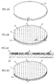
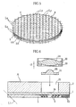
- FIG. 3A ⁇ 3B, 4A ⁇ 4D, 5 and 6 illustrate a fabrication method of the above-described optical head Hd. As seen from the explanation given below, a plurality of identical optical heads can be collectively produced by the fabrication method.
- a first wafer 1A and a second wafer 2A are prepared.
- the first wafer 1A is formed with a plurality of coils 4 and insulating protection layer 5 in its upper surface.
- the first wafer 1A may be prepared in the following procedure.
- a transparent glass disk 1A' For producing the first wafer 1A, use is made of a transparent glass disk 1A', as shown in Fig. 4A.
- the glass disk 1A' has a thickness tl.
- a plurality of coils 4 are formed in a matrix layout.
- Such a coil may be produced in several ways. One way is as follows: A photoresist layer is formed on the glass disk 1A', and a spiral groove (corresponding to the desired coil element) is formed in the resist layer. Then, a conductive coil body is formed in the spiral groove by plating. Another way is to use sputtering or evaporation.
- the coil 4 has a two-layer structure consisting of first and second spiral elements.
- the coil 4 is produced through several steps which include: a first step of forming the first spiral element; a second step of forming a protection layer to cover the first spiral element; a third step of forming the second spiral element on the protection layer; and a fourth step of forming an additional protection layer to cover the second spiral element.
- a connection forming step is also included for connecting the first and the second spiral elements to each other.
- the protection layer 5 may be obtained by sputtering or ion-plating.
- the protection layer 5 has a thickness of about 8 ⁇ m for example.
- the bottom of the glass disk 1A' is subjected to grinding so that the thickness of the disk is reduced to t2, as shown in Fig. 4D.
- the first wafer 1A is obtained.
- the thickness t2 depends on the thickness of the second lens 3B. Specifically, the thickness t2 is determined so that the total thickness of the processed glass disk 1A' and the second lens 3B becomes equal to the required value. In the illustrated example, the thickness t2 is about 0.2mm.
- the second wafer 2A is the matrix from which the lens holder 2 as shown in Figs. 1 and 2 is produced.
- the thickness of the wafer 2A is about 0.6mm for example.
- the wafer 2A is formed with a plurality of through-holes 20 corresponding in position to the coils 4 formed on the first wafer 1A.
- Each through-hole 20 may be formed in the following manner. First, a small preliminary hole is made in the wafer 2A by laser processing for example. A conductive wire for electro-discharge machining is put through the preliminary hole. Then, voltage is applied to the wire so that the preliminary hole is enlarged up to the size of the desired through-hole 20.
- the first and the second wafers 1A, 2A are joined with glue.
- the bottom surface of the first wafer 1A is attached to one side of the second wafer 2A in a manner such that the center of the respective coils 4 coincides with the center of the relevant one of the through-holes 20.
- Each prototype A' includes a transparent plate 1 and a lens holder 2 attached to the plate 1. On its lower side, the plate 1 is formed with a coil 4 and an insulating protection layer 5 enclosing the coil 4.
- the transparent plate 1 stems from the first wafer 1A, while the lens holder 2 stems from the second wafer 2A.
- the prototype A' is subjected to chamfering for forming the slant surface 19 (see Fig. 2 and line L1 in Fig. 6).
- the prototype A' is also subjected to electrode-forming for providing the electrodes 41 connected to the leads 40 of the coil 4 (see Fig. 2).
- a first lens 3A and a second lens 3B are installed to the lens holder 2 of the prototype A'.
- the second lens 3B is put in the through-hole 20 and then glued to the upper surface 1b of the transparent plate 1.
- the first lens 3A is mounted on the lens holder 2 through a lens attachment 39 which is glued to the upper surface of the lens holder.
- the positions of the respective lenses are monitored by optical means, so that the center of each lens will be aligned with the center of the coil 4.
- the distance between the first and the second lenses 3A, 3B is defined by the thickness of the lens holder 2 and the thickness t3 of the lens attachment 39. However, this distance may be adjusted by shifting the lens attachment 39 relative to the lens holder 2 by e.g. interposing a suitable spacer between the attachment 39 and the holder 2. In this manner, the focus of the lens system can be adjusted properly.
- the optical head Hd shown in Figs. 1 and 2 is obtained with great productivity due to the collective production of a number of identical optical heads.
- the installation of the first and the second lenses 3A, 3B is performed after the cutting of the wafers 1A, 2A.
- This order is advantageous to preventing the lenses 3A and 3B from being damaged during the wafer cutting procedure.
- the present invention is not limited to this, and the order may be reversed.
- optical head Hd The function and advantages of the optical head Hd will now be described below.
- the basic function of the optical head Hd of the present invention is the same as that of a conventional optical head.
- the optical head Hd serves as a slider designed to float slightly above the MO disk D rotating at high speed.
- the laser beam emitted from a light source (not shown) is caused to converge as passing through the first and the second lenses 3A and 3B, whereby a small light spot is formed on the recording layer 99 of the disk D.
- the coil 4 generates a magnetic field required for performing data-writing by magnetic field modulation.
- the flat lens surface of the second lens 3B is attached to the upper surface 1b of the transparent plate 1, and this upper surface is attached to the flat bottom surface 2a of the lens holder 2.
- the second lens 3B can be easily positioned in a non-slanting manner relative to the bottom surface 2a of the holder 2. Accordingly, coma (which would otherwise occur due to the tilting of the second lens 3B) will be prevented from occurring, and the diameter of the light spot on the recording layer 99 is advantageously small.
- the close-fitting of the flange 31 with the through-hole 20 facilitates the center alignment between the second lens 3B and the through-hole 20. In inserting the second lens 3B into the through-hole 20, the flange 31 may be grasped so that the functional lens surfaces of the lens 3B will not be damaged.
- the lens attachment 39 is attached to the upper surface 2b of the lens holder 2.
- the first lens 3A can be installed in a non-slanting manner relative to the lower surface 2a of the lens holder 2.
- coma which would otherwise be caused by the tilting of the first lens 3A, is prevented from occurring.
- the distance between the first and the second lenses 3A, 3B can be adjusted by changing the thickness of the holder 2.
- the wavelength of semiconductor laser may vary with temperature.
- the refractive index of the object lens system will change.
- the laser beam may fail to be properly focused onto the desired portion of the storage disk.
- the objective lens system may be composed as an achromatic lens system by using a converging lens and a diverging lens in combination.
- the lens system of the present invention may include a third lens in addition to the first and the second lenses.
- a lens of the lens system may be provided with a hologram (diffracting grating) for coping with the wavelength variation of the laser beam.
- two optical heads Hd may be used for one MO disk D provided with two recording layers (not shown) facing upward and downward.
- the optical heads Hd are arranged symmetrically to each other with respect to the disk D.
- the both heads Hd are moved together in parallel to the disk D, so that the mutually facing relation across the disk D is maintained. In this manner, it is possible to cancel out the pressing forces exerted on the disk D by the two heads Hd. This is advantageous to preventing the warping of the disk D.
Landscapes
- Physics & Mathematics (AREA)
- Optics & Photonics (AREA)
- Optical Head (AREA)
Applications Claiming Priority (2)
| Application Number | Priority Date | Filing Date | Title |
|---|---|---|---|
| JP2001334326 | 2001-10-31 | ||
| JP2001334326A JP3950318B2 (ja) | 2001-10-31 | 2001-10-31 | 光学ヘッドおよびその製造方法 |
Publications (2)
| Publication Number | Publication Date |
|---|---|
| EP1308947A2 true EP1308947A2 (de) | 2003-05-07 |
| EP1308947A3 EP1308947A3 (de) | 2006-02-01 |
Family
ID=19149474
Family Applications (1)
| Application Number | Title | Priority Date | Filing Date |
|---|---|---|---|
| EP02250683A Withdrawn EP1308947A3 (de) | 2001-10-31 | 2002-01-31 | Optischer Kopf und Verfahrung zur seinen Herstellung |
Country Status (3)
| Country | Link |
|---|---|
| US (1) | US6717905B2 (de) |
| EP (1) | EP1308947A3 (de) |
| JP (1) | JP3950318B2 (de) |
Cited By (1)
| Publication number | Priority date | Publication date | Assignee | Title |
|---|---|---|---|---|
| WO2009088297A3 (en) * | 2008-01-04 | 2009-10-29 | Benestad Paal G | Sensor and detection device for use of the sensor |
Families Citing this family (2)
| Publication number | Priority date | Publication date | Assignee | Title |
|---|---|---|---|---|
| KR101002373B1 (ko) * | 2003-06-17 | 2010-12-17 | 아이노셉 엑스 홀딩스 엘엘씨 | 초점 심도 조절용 마이크로 액츄에이터 |
| WO2005104096A1 (en) * | 2004-04-23 | 2005-11-03 | Koninklijke Philips Electronics N.V. | Magneto optical device |
Family Cites Families (10)
| Publication number | Priority date | Publication date | Assignee | Title |
|---|---|---|---|---|
| EP0979508A4 (de) * | 1997-04-29 | 2001-10-24 | Terastor Corp | Elektrooptisches speichersystem mit fliegendem kopf für nahfeldaufzeichnung und wiedergabe |
| JPH11242801A (ja) | 1998-02-26 | 1999-09-07 | Sony Corp | 光磁気ディスク装置とこれに使用される磁界発生装置及びその製造方法 |
| US6351436B1 (en) * | 1998-05-11 | 2002-02-26 | Maxtor Corporation | Field enhancing magnetic pole for magneto-optical recording and reproducing device |
| JP3393067B2 (ja) * | 1998-06-30 | 2003-04-07 | 富士通株式会社 | 光ディスク装置用光学ヘッド |
| US6657927B1 (en) * | 1998-08-04 | 2003-12-02 | Hitachi Maxell, Ltd. | Optical head and apparatus provided therewith |
| US6049430A (en) * | 1998-11-12 | 2000-04-11 | Seagate Technology | High numerical aperture objective lens manufacturable in wafer form |
| US6094803A (en) * | 1999-01-21 | 2000-08-01 | Read-Rite Corporation | Wafer processing techniques for near field magneto-optical head |
| JP2001023260A (ja) * | 1999-07-08 | 2001-01-26 | Sony Corp | 磁界変調用磁気ヘッド、磁気光学素子、光学ピックアップ装置および光ディスク装置 |
| JP3540678B2 (ja) | 1999-08-25 | 2004-07-07 | 富士通株式会社 | 光学ヘッド |
| US6529449B1 (en) * | 2000-07-26 | 2003-03-04 | Aiwa Co. Ltd. | Magneto-optical head involving solid immersion lens with two-layer heat-dispersive coil |
-
2001
- 2001-10-31 JP JP2001334326A patent/JP3950318B2/ja not_active Expired - Fee Related
-
2002
- 2002-01-28 US US10/058,720 patent/US6717905B2/en not_active Expired - Fee Related
- 2002-01-31 EP EP02250683A patent/EP1308947A3/de not_active Withdrawn
Cited By (1)
| Publication number | Priority date | Publication date | Assignee | Title |
|---|---|---|---|---|
| WO2009088297A3 (en) * | 2008-01-04 | 2009-10-29 | Benestad Paal G | Sensor and detection device for use of the sensor |
Also Published As
| Publication number | Publication date |
|---|---|
| US20030081529A1 (en) | 2003-05-01 |
| JP2003141792A (ja) | 2003-05-16 |
| EP1308947A3 (de) | 2006-02-01 |
| JP3950318B2 (ja) | 2007-08-01 |
| US6717905B2 (en) | 2004-04-06 |
Similar Documents
| Publication | Publication Date | Title |
|---|---|---|
| US6130779A (en) | Near field magneto-optical head made using wafer processing techniques | |
| US6094803A (en) | Wafer processing techniques for near field magneto-optical head | |
| CN1129023C (zh) | 集成微光学系统 | |
| US6781926B2 (en) | Magneto-optical head having heat sink layer | |
| US6542281B2 (en) | Integrated micro-optical systems | |
| KR100636862B1 (ko) | 광학 헤드용 슬라이더 | |
| EP1489606A1 (de) | Optisches Abtastgerät mit verbesserten optischen Eigenschaften, und Herstellungsverfahren des optischen Abtastgerätes | |
| US6827802B2 (en) | Optical recording head having a solid immersion lens | |
| US6631099B1 (en) | Magnetic field modulation magnetic head, magneto-optical element, optical pickup device, and optical disk drive, in which first and second magnetic cores are placed on opposite sides of magnetic field generation coil to achieve low power consumption and high efficiency | |
| US6717905B2 (en) | Optical head and method of making the same | |
| US6762978B2 (en) | Optical head slider, method for manufacturing optical head slider, and recording and/or reproducing apparatus | |
| EP1026676B1 (de) | Linsenanordnung und deren Verwendung in einem optischen Abtastkopf | |
| US6757221B1 (en) | Optical head having object lens and patterned coil | |
| CN1310231C (zh) | 光学拾取器装置,光盘装置和光学拾取器调整方法 | |
| JP2000149284A (ja) | ビ―ム照射装置と、フォ―カス制御装置と、情報記録媒体に対するビ―ム照射装置を有する光学装置と、情報記録媒体用原盤の製造方法と、情報記録媒体の製造方法 | |
| US8059345B2 (en) | Integrated micro-optical systems | |
| JP2002350609A (ja) | 光学素子作製方法、光学素子および光ピックアップ装置 | |
| JP2001014708A (ja) | レンズ付きスライダ及びその製造方法 | |
| WO2011158413A1 (ja) | 光ヘッド、光学素子、及び情報記録装置 |
Legal Events
| Date | Code | Title | Description |
|---|---|---|---|
| PUAI | Public reference made under article 153(3) epc to a published international application that has entered the european phase |
Free format text: ORIGINAL CODE: 0009012 |
|
| AK | Designated contracting states |
Designated state(s): AT BE CH CY DE DK ES FI FR GB GR IE IT LI LU MC NL PT SE TR |
|
| AX | Request for extension of the european patent |
Extension state: AL LT LV MK RO SI |
|
| PUAL | Search report despatched |
Free format text: ORIGINAL CODE: 0009013 |
|
| AK | Designated contracting states |
Kind code of ref document: A3 Designated state(s): AT BE CH CY DE DK ES FI FR GB GR IE IT LI LU MC NL PT SE TR |
|
| AX | Request for extension of the european patent |
Extension state: AL LT LV MK RO SI |
|
| 17P | Request for examination filed |
Effective date: 20060320 |
|
| AKX | Designation fees paid |
Designated state(s): DE GB |
|
| 17Q | First examination report despatched |
Effective date: 20090318 |
|
| STAA | Information on the status of an ep patent application or granted ep patent |
Free format text: STATUS: THE APPLICATION IS DEEMED TO BE WITHDRAWN |
|
| 18D | Application deemed to be withdrawn |
Effective date: 20090729 |