EP1296452A1 - Anpassungsschaltung fur Funkantenne - Google Patents
Anpassungsschaltung fur Funkantenne Download PDFInfo
- Publication number
- EP1296452A1 EP1296452A1 EP01850160A EP01850160A EP1296452A1 EP 1296452 A1 EP1296452 A1 EP 1296452A1 EP 01850160 A EP01850160 A EP 01850160A EP 01850160 A EP01850160 A EP 01850160A EP 1296452 A1 EP1296452 A1 EP 1296452A1
- Authority
- EP
- European Patent Office
- Prior art keywords
- port
- radiator
- transmission circuit
- impedance
- frequency band
- Prior art date
- Legal status (The legal status is an assumption and is not a legal conclusion. Google has not performed a legal analysis and makes no representation as to the accuracy of the status listed.)
- Withdrawn
Links
- 230000005540 biological transmission Effects 0.000 claims abstract description 37
- 239000003990 capacitor Substances 0.000 claims description 17
- 230000005855 radiation Effects 0.000 claims description 4
- 238000013461 design Methods 0.000 claims description 2
- 230000010363 phase shift Effects 0.000 claims description 2
- 230000005404 monopole Effects 0.000 abstract description 10
- 238000010586 diagram Methods 0.000 description 9
- 230000008878 coupling Effects 0.000 description 7
- 238000010168 coupling process Methods 0.000 description 7
- 238000005859 coupling reaction Methods 0.000 description 7
- 230000001939 inductive effect Effects 0.000 description 4
- 230000001427 coherent effect Effects 0.000 description 2
- 230000007423 decrease Effects 0.000 description 2
- 238000005259 measurement Methods 0.000 description 2
- 230000009466 transformation Effects 0.000 description 2
- 238000006243 chemical reaction Methods 0.000 description 1
- 239000004020 conductor Substances 0.000 description 1
- 238000011161 development Methods 0.000 description 1
- 230000000694 effects Effects 0.000 description 1
- 239000002184 metal Substances 0.000 description 1
- 238000000034 method Methods 0.000 description 1
- 230000000737 periodic effect Effects 0.000 description 1
- 238000012545 processing Methods 0.000 description 1
- 230000001681 protective effect Effects 0.000 description 1
- 238000012546 transfer Methods 0.000 description 1
Images


Classifications
-
- H—ELECTRICITY
- H03—ELECTRONIC CIRCUITRY
- H03H—IMPEDANCE NETWORKS, e.g. RESONANT CIRCUITS; RESONATORS
- H03H7/00—Multiple-port networks comprising only passive electrical elements as network components
- H03H7/38—Impedance-matching networks
- H03H7/383—Impedance-matching networks comprising distributed impedance elements together with lumped impedance elements
Definitions
- the object of the invention is to provide a radio antenna that includes a matching circuit which functions on at least two different frequency bands, of which at least one is broad.
- the antenna shall be relatively small in relation to alternative solutions, and that it shall be relatively simple and economic to mass-produce.
- the matching circuit can be mounted on printed circuit boards. In some cases, the radiator may also be mounted on the same printed circuit board.
- the invention has evolved as a result of the need to transmit and receive radio waves with a single antenna, within all of the following communications frequency band: GSM 890 - 960 MHz GSM 1710 - 1880 MHz GSM 1850 - 1990 MHz DECT 1880 - 1900 MHz UMTS 1900 - 2200 MHz
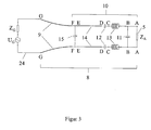
- a complete antenna consists of radiator (5, 20) and matching circuit (8).
- the matching circuit always includes a transmission circuit (10, 21) and, when required, a Balun transformer (9). It is assumed that the radiator has low radiation resistance within a first frequency band and a high radiation resistance within a second frequency band.
- the purpose of the transmission circuit (10, 21) is to transfer the electromagnetic wave from the antenna connection point, Port A-A, to the other end of the transmission circuit, Port F-F, so that its impedance values within both frequency bands will lie in the proximity of a common resistance value that corresponds to the impedance of the feeder, the Balun transformer, or the radio apparatus, illustrated at point O in the Smith chart of Figures 4 to 8 inclusive.
- the matching circuit (8) will also include a Balun transformer (9) whose Port G-G is matched to the unbalanced feeder.
- the impedance of the radiator (5) in the Smith chart shows that the curve intersects the true axis at a first point (P) within the first frequency band, and at a second point (Q) within the second frequency band.
- the radiator (5) is thus resonant at these frequencies.
- the curve is moved down in the capacitive region of the Smith chart shown in Figure 5, with the aid of parallel capacitor (11).
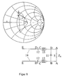
- the inductance (13) moves the curve to the inductive region and draws the curve together to form a small loop in accordance with Figure 6.
- the curve is moved closer to the centre point (O) of the diagram in Figure 7, with the aid of series capacitor (12), and its balance is improved in relation to the horizontal axis (X) of the diagram at the same time.
- the transmission circuit (10) is comprised of parallel capacitor (11), series inductance (13), series capacitor (12), phase shifting line (14) and parallel capacitor (15), in that order.
- the Balun transformer (9) will be described below in conjunction with the first preferred embodiment.
- Small two band radiators for frequency bands around 900 MHz and 1800 MHz are available commercially although they are not sufficiently broadbanded to reach to frequencies of 2200 MHz. Further, very high broadband antennas are available, for instance the logarithmic periodic antennas, although these are too large and expensive for simpler applications.
- a two frequency impedance matching circuit is a matching circuit for a simple whip antenna that enables roughly 50 Ohms matching at two frequencies to be achieved. In the preferred embodiment, these frequencies lie between 810 and 960 MHz. This implies that the antenna is broadbanded within this frequency band; see Fig. 7 of the patent specification.
- the present invention has a different aim, as matching is strived for in two frequency bands that are widely separate from each other, of which at least one band is very wide. 3
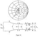
- Figure 10 illustrates the Smith chart of the entire antenna at port G-G in the first preferred embodiment, where an unbalanced feeder from the transceiver (not shown in the figure) can be connected.
- Figure 11 illustrates an antenna with unbalanced radiator in a second preferred embodiment.
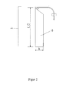
- the antenna (1) shown in Figure 1 comprises two parts:
- Both components are mounted on a printed circuit board (2) that has respective first and second sides (3 and 4). Both sides are metallised and carry printed patterns.
- radiator (5) a dipole that has a first resonance point (P), see Figure 4, in the first frequency band (where it functions as a half-wave dipole) and a second resonance point (Q) in the second frequency band (where it functions as a full-wave dipole).
- P first resonance point
- Q second resonance point
- This radiator is balanced.
- the measurement ratio between the width (B) of the dipole, see Figure 2, and the length (I) is sufficiently large to cover the first frequency band.
- One dipole half is mounted on the first side of the printed circuit board, and the other dipole half on its other side. This enables the matching circuit and feeder (in the form of a microstrip) to be included in the pattern on said board.
- radiator means that its impedance in the gap will be approximately 60 Ohms in the first band and approximately 500 Ohms in the second band; see Figure 4.
- the antenna is constructed for a microstrip feeder that has characteristic impedance of 50 Ohms.
- the imbalance must be compensated for, when a microstrip or a coaxial conductor is unbalanced (non-symmetrical), whereas a dipole is balanced (symmetrical).
- the impedance difference in the second band must also be compensated for, and hence a matching circuit is necessary.
- the matching circuit (8) for the first preferred embodiment consists of two parts:
- the Balun transformer and the transmission circuit are connected in series.
- a resistance of 75 Ohms with the smallest possible reactance was taken as a choice of impedance at the connecting point (Port F-F) between the transmission circuit (10) and the Balun transformer (9).
- the transmission circuit (10) transforms the impedance from Port A-A to Port F-F so that it increases slightly in the first band and decreases more in the second band. As a result, the impedance lands in the vicinity of the same value at all frequencies lying in the frequency bands in question, this value being 75 Ohms, for instance.
- the Balun transformer (9) is constructed so that transformation takes place from 75 Ohms, balanced port (F-F) to 50 Ohms, unbalanced port (G-G).
- the modified Klopfenstein type is so broadbanded that its ports retain the same impedance within both frequency bands.
- the transmission circuit (10) consists of a parallel capacitor (11), two series inductances (13), two series capacitors (12), a phase shifting line (14), and a parallel capacitor (15), in that order.
- the reason why the series components are in pairs - something that is generally unnecessary - is because it is desired to maintain the symmetry in the structure between the dipole (5) and the Balun transformer (9).
- Each component in the transmission circuit changes the impedance curve in the Smith chart in its own way, as described hereinafter and illustrated to 50 Ohms.
- the impedance ( Figure 4) of the dipole (5) shows that the curve intersects the real axis X at the following points: 60 Ohms in the first band (P) and 500 Ohms in the second band (Q). The dipole is thus resonant at these frequencies.
- the curve is moved downwards into the capacitive region of the Smith chart according to Figure 5, with the aid of a parallel capacitor (11).
- the inductances (13) move the curve to the inductive region and draw the curve together to form a small loop as small loop as shown in Figure 6.
- the curve is moved closer to the centre point (O) of the chart with the aid of series capacitors (12), therewith improving the balance of the curve in relation to the horizontal axis (X), see Figure 7.
- the antenna (16) shown in Figure 11 consists of two parts:
- radiator (20) a monopole over the earth plane (19, 23), having a first resonance point in the first frequency band (here it functions as a quarter-wave monopole) and with a second resonance point in the other frequency band (where it functions as a half-wave monopole).
- the measurement ratio between the width (b) and the length (k) of the monopole is chosen to be large enough to cover the first frequency band.
- the transmission circuit (21) is mounted on a printed circuit board (17) that has a first and a second side (18 and 19 respectively). Both sides are metallised and carry patterns.
- the radiator is placed perpendicular to the first side of the printed circuit board (17), the metal pattern on said first side (18) being one side of the transmission circuit (21).
- the other side of the transmission circuit (21) and part of the earth plane are mounted on the other side (19) of the printed circuit board.
- the feeder (22) in the form of a microstrip can also be mounted on the printed circuit board (17).
- a Balun transformer is not required for monopole radiators.
- radiator (20) means that its impedance in the gap will be approximately 30 Ohms in the first band and approximately 300 Ohms in the second band.
- the antenna is constructed for feeding with an unbalanced line that has a characteristic impedance of 50 Ohms.
- the transmission circuit is also needed in this case for impedance matching in the second band. No Balun transformer is required on the other hand.
- the impedance at the connection point (Port F-F) between the transmission circuit (21) and the feeder (22) in this example will preferably have a resistance of 50 Ohms and the smallest possible reactance.
- the transmission circuit is designed to transform impedances in the following manner: Port A-A Port F-F VSWR without transmissioncircuit First band 30 Ohms 50 Ohms 1:1.67 Second band 300 Ohms 50 Ohms 1:6
- the transmission circuit transforms impedance from Port A-A to Port F-F so that it increases slightly in the first band and decreases significantly in the second band.
- the impedance will lie in the proximity of the same value, in this example 50 Ohms, at all frequencies that lie in the frequency bands concerned.
- the principles for processing the curve in the Smith charts described in connection with the first preferred embodiment also apply here.
- the Smith charts can suitably be normalised to 50 Ohms.
Landscapes
- Details Of Aerials (AREA)
Priority Applications (2)
| Application Number | Priority Date | Filing Date | Title |
|---|---|---|---|
| EP01850160A EP1296452A1 (de) | 2001-09-20 | 2001-09-20 | Anpassungsschaltung fur Funkantenne |
| US09/956,831 US6664934B2 (en) | 2001-09-20 | 2001-09-21 | Radio antenna matching circuit |
Applications Claiming Priority (2)
| Application Number | Priority Date | Filing Date | Title |
|---|---|---|---|
| EP01850160A EP1296452A1 (de) | 2001-09-20 | 2001-09-20 | Anpassungsschaltung fur Funkantenne |
| US09/956,831 US6664934B2 (en) | 2001-09-20 | 2001-09-21 | Radio antenna matching circuit |
Publications (1)
| Publication Number | Publication Date |
|---|---|
| EP1296452A1 true EP1296452A1 (de) | 2003-03-26 |
Family
ID=26077515
Family Applications (1)
| Application Number | Title | Priority Date | Filing Date |
|---|---|---|---|
| EP01850160A Withdrawn EP1296452A1 (de) | 2001-09-20 | 2001-09-20 | Anpassungsschaltung fur Funkantenne |
Country Status (2)
| Country | Link |
|---|---|
| US (1) | US6664934B2 (de) |
| EP (1) | EP1296452A1 (de) |
Families Citing this family (5)
| Publication number | Priority date | Publication date | Assignee | Title |
|---|---|---|---|---|
| GB0204108D0 (en) * | 2002-02-21 | 2002-04-10 | Analog Devices Inc | 3G radio |
| FR2837988B1 (fr) * | 2002-03-26 | 2008-06-20 | Thales Sa | Systeme antennaire bi-bande vhf-uhf |
| JP5304890B2 (ja) * | 2009-04-01 | 2013-10-02 | 株式会社村田製作所 | アンテナ整合回路、アンテナ装置及びアンテナ装置の設計方法 |
| US8487821B2 (en) * | 2009-06-08 | 2013-07-16 | Symbol Technologies, Inc. | Methods and apparatus for a low reflectivity compensated antenna |
| DE202015009937U1 (de) * | 2014-04-11 | 2021-10-28 | Commscope Technologies Llc | Mehrbandstrahler-Arrays mit eliminierten Resonanzen |
Citations (2)
| Publication number | Priority date | Publication date | Assignee | Title |
|---|---|---|---|---|
| EP0613209A1 (de) * | 1993-02-26 | 1994-08-31 | Nec Corporation | Schaltungsanordnung zur Impedanzanpassung für zwei Frequenzen für eine Antenne |
| US6278340B1 (en) * | 1999-05-11 | 2001-08-21 | Industrial Technology Research Institute | Miniaturized broadband balun transformer having broadside coupled lines |
Family Cites Families (3)
| Publication number | Priority date | Publication date | Assignee | Title |
|---|---|---|---|---|
| US5528252A (en) | 1994-10-26 | 1996-06-18 | Ntl Technologies Inc. | Dipole television antenna |
| US5652599A (en) * | 1995-09-11 | 1997-07-29 | Qualcomm Incorporated | Dual-band antenna system |
| US6078794A (en) | 1997-02-19 | 2000-06-20 | Motorola, Inc. | Impedance matching for a dual band power amplifier |
-
2001
- 2001-09-20 EP EP01850160A patent/EP1296452A1/de not_active Withdrawn
- 2001-09-21 US US09/956,831 patent/US6664934B2/en not_active Expired - Fee Related
Patent Citations (2)
| Publication number | Priority date | Publication date | Assignee | Title |
|---|---|---|---|---|
| EP0613209A1 (de) * | 1993-02-26 | 1994-08-31 | Nec Corporation | Schaltungsanordnung zur Impedanzanpassung für zwei Frequenzen für eine Antenne |
| US6278340B1 (en) * | 1999-05-11 | 2001-08-21 | Industrial Technology Research Institute | Miniaturized broadband balun transformer having broadside coupled lines |
Non-Patent Citations (5)
| Title |
|---|
| DEHONEY R J: "PROGRAM SYNTHESIZES ANTENNA MATCHING NETWORKS FOR MAXIMUM BANDWIDTH", RF DESIGN, CARDIFF PUBLISHING CO, ENGLEWOOD,CO, US, vol. 18, no. 5, 1 May 1995 (1995-05-01), pages 74,76,78,81, XP000505469, ISSN: 0163-321X * |
| LI L C C ET AL: "VLF/LF coupler and antenna modeling", MILITARY COMMUNICATIONS CONFERENCE, 1989. MILCOM '89., vol. 2, 15 November 1989 (1989-11-15) - 18 November 1989 (1989-11-18), Boston, MA, USA, pages 585 - 592, XP010083514 * |
| NEMLIKHER YU A ET AL: "OCTAVE TRANSFORMERS OF IMPEDANCES EMPLOYING LC ELEMENTS", TELECOMMUNICATIONS AND RADIO ENGINEERING, BEGELL HOUSE, INC., NEW YORK, NY, US, vol. 47, no. 1, 1992, pages 120 - 123, XP000316424, ISSN: 0040-2508 * |
| NURNBERGER M W ET AL: "NEW TECHNIQUES FOR EXTREMELY BROADBAND PLANAR SLOT SPIRAL ANTENNAS", IEEE ANTENNAS AND PROPAGATION SOCIETY INTERNATIONAL SYMPOSIUM. 1999 DIGEST. APS. ORLANDO, FL, JULY 11 - 16, 1999, NEW YORK, NY: IEEE, US, vol. 4, 11 July 1999 (1999-07-11), pages 2690 - 2693, XP000935583, ISBN: 0-7803-5640-3 * |
| YARMAN B S ET AL: "COMPUTER-AIDED DOUBLE MATCHING VIA PARAMETRIC REPRESENTATION OF BRUNE FUNCTIONS", IEEE TRANSACTIONS ON CIRCUITS AND SYSTEMS, IEEE INC. NEW YORK, US, vol. 37, no. 2, 1 February 1990 (1990-02-01), pages 212 - 222, XP000127772 * |
Also Published As
| Publication number | Publication date |
|---|---|
| US6664934B2 (en) | 2003-12-16 |
| US20030058184A1 (en) | 2003-03-27 |
Similar Documents
| Publication | Publication Date | Title |
|---|---|---|
| US6922172B2 (en) | Broad-band antenna for mobile communication | |
| US6271796B1 (en) | Built-in antenna for radio communication terminals | |
| US5835063A (en) | Monopole wideband antenna in uniplanar printed circuit technology, and transmission and/or recreption device incorporating such an antenna | |
| US7088299B2 (en) | Multi-band antenna structure | |
| US6094178A (en) | Dual mode quadrifilar helix antenna and associated methods of operation | |
| CN101553953B (zh) | 天线装置 | |
| US5313218A (en) | Antenna assembly | |
| US8144072B2 (en) | Multi-band antenna for notebook computer | |
| US20020140607A1 (en) | Internal multi-band antennas for mobile communications | |
| US5914695A (en) | Omnidirectional dipole antenna | |
| US6894648B2 (en) | Antenna apparatus and a portable wireless communication apparatus using the same | |
| US10992047B2 (en) | Compact folded dipole antenna with multiple frequency bands | |
| WO2004062033A1 (en) | Meander line antenna coupler and shielded meander line | |
| CN112003022A (zh) | 一种满足北斗卫星导航的双频圆极化微带天线 | |
| Alibakhshikenari et al. | Impedance matching network based on metasurfaces (2-D metamaterials) for electrically small antennas | |
| WO2018157661A1 (zh) | 天线和终端 | |
| EP1188200B1 (de) | Flache monopolantenne | |
| US6664934B2 (en) | Radio antenna matching circuit | |
| EP0474490B1 (de) | Antennenanordnung | |
| KR20020019616A (ko) | 임피던스 정합 회로 및 안테나 장치 | |
| US20200136258A1 (en) | Multi-band planar antenna | |
| CN212342814U (zh) | 印刷天线及电子设备 | |
| CN107946772A (zh) | 一种新型双频缝隙谐振天线 | |
| KR100861865B1 (ko) | 무선 단말기 | |
| US6570544B2 (en) | Radiator components that serve to transmit information over frequencies in range with one or more octaves less than or equal to thirty megahertz and that comprise major dimension less than or equal to nine meters |
Legal Events
| Date | Code | Title | Description |
|---|---|---|---|
| PUAI | Public reference made under article 153(3) epc to a published international application that has entered the european phase |
Free format text: ORIGINAL CODE: 0009012 |
|
| AK | Designated contracting states |
Kind code of ref document: A1 Designated state(s): AT BE CH CY DE DK ES FI FR GB GR IE IT LI LU MC NL PT SE TR Designated state(s): AT BE CH CY DE DK ES FI FR GB GR IE IT LI LU MC NL PT SE TR |
|
| AX | Request for extension of the european patent |
Extension state: AL LT LV MK RO SI |
|
| 17P | Request for examination filed |
Effective date: 20030926 |
|
| AKX | Designation fees paid |
Designated state(s): DE GB IT |
|
| 17Q | First examination report despatched |
Effective date: 20061214 |
|
| STAA | Information on the status of an ep patent application or granted ep patent |
Free format text: STATUS: THE APPLICATION IS DEEMED TO BE WITHDRAWN |
|
| 18D | Application deemed to be withdrawn |
Effective date: 20110628 |