EP1296371A2 - Semiconductor device and method of making the same - Google Patents
Semiconductor device and method of making the same Download PDFInfo
- Publication number
- EP1296371A2 EP1296371A2 EP02020768A EP02020768A EP1296371A2 EP 1296371 A2 EP1296371 A2 EP 1296371A2 EP 02020768 A EP02020768 A EP 02020768A EP 02020768 A EP02020768 A EP 02020768A EP 1296371 A2 EP1296371 A2 EP 1296371A2
- Authority
- EP
- European Patent Office
- Prior art keywords
- package
- housing
- semiconductor device
- polyamide
- thermoplastic resin
- Prior art date
- Legal status (The legal status is an assumption and is not a legal conclusion. Google has not performed a legal analysis and makes no representation as to the accuracy of the status listed.)
- Withdrawn
Links
Images


Classifications
-
- H—ELECTRICITY
- H10—SEMICONDUCTOR DEVICES; ELECTRIC SOLID-STATE DEVICES NOT OTHERWISE PROVIDED FOR
- H10W—GENERIC PACKAGES, INTERCONNECTIONS, CONNECTORS OR OTHER CONSTRUCTIONAL DETAILS OF DEVICES COVERED BY CLASS H10
- H10W74/00—Encapsulations, e.g. protective coatings
- H10W74/40—Encapsulations, e.g. protective coatings characterised by their materials
- H10W74/47—Encapsulations, e.g. protective coatings characterised by their materials comprising organic materials, e.g. plastics or resins
-
- H—ELECTRICITY
- H10—SEMICONDUCTOR DEVICES; ELECTRIC SOLID-STATE DEVICES NOT OTHERWISE PROVIDED FOR
- H10W—GENERIC PACKAGES, INTERCONNECTIONS, CONNECTORS OR OTHER CONSTRUCTIONAL DETAILS OF DEVICES COVERED BY CLASS H10
- H10W74/00—Encapsulations, e.g. protective coatings
- H10W74/10—Encapsulations, e.g. protective coatings characterised by their shape or disposition
- H10W74/111—Encapsulations, e.g. protective coatings characterised by their shape or disposition the semiconductor body being completely enclosed
- H10W74/121—Encapsulations, e.g. protective coatings characterised by their shape or disposition the semiconductor body being completely enclosed by multiple encapsulations, e.g. by a thin protective coating and a thick encapsulation
-
- H—ELECTRICITY
- H10—SEMICONDUCTOR DEVICES; ELECTRIC SOLID-STATE DEVICES NOT OTHERWISE PROVIDED FOR
- H10W—GENERIC PACKAGES, INTERCONNECTIONS, CONNECTORS OR OTHER CONSTRUCTIONAL DETAILS OF DEVICES COVERED BY CLASS H10
- H10W74/00—Encapsulations, e.g. protective coatings
- H10W74/10—Encapsulations, e.g. protective coatings characterised by their shape or disposition
- H10W74/111—Encapsulations, e.g. protective coatings characterised by their shape or disposition the semiconductor body being completely enclosed
- H10W74/127—Encapsulations, e.g. protective coatings characterised by their shape or disposition the semiconductor body being completely enclosed characterised by arrangements for sealing or adhesion
Definitions
- the present invention relates to sealing of a semiconductor device in which a semiconductor package and a housing containing the semiconductor package are formed of different synthetic resins. More particularly, the present invention relates to a semiconductor device in which a housing is formed of thermoplastic resin (a first synthetic resin) and a semiconductor package is formed of thermosetting epoxy resin (a second synthetic resin), and a method of making the same.
- thermosetting epoxy resin which is a raw material of the semiconductor package
- thermoplastic resin which is a raw material of the housing
- a semiconductor device has been made by a method different from insert molding.
- a housing 51 having a connector terminal 50 is provided.
- the connector terminal 50 is preformed by injection molding in a predetermined position of the housing 51.
- a surface of the package 52 that abuts against the housing 51 has an adhesive agent applied thereon.
- the connecting portion 52a of the package 52 is placed in contact with the connector terminal 50, the package 52 is fixed to the housing 51.
- a space 53 in the housing 51 is filled with a sealant 54 such as liquid epoxy and silicone to seal the package 52.
- the above-mentioned manufacturing method in which the package 52 is sealed with the sealant 54, requires more steps (i.e. three steps) compared to the manufacturing method by insert molding: a step of making the housing 51 having the connector terminal 50, a step of adhering the package 52 to the housing 51, and a step -of filling the housing 51 with the sealant 54. This complicates the manufacturing process as well as increases the manufacturing costs of the semiconductor device.
- An object of the invention is to provide a semiconductor device that is easy to manufacture and has excellent moisture resistance.
- Another object of the invention is to provide a semiconductor device that holds down its manufacturing costs.
- the semiconductor device includes a housing formed of a first synthetic resin that is a thermoplastic resin and a semiconductor package formed of a second synthetic resin that is a thermosetting resin.
- the package is sealed in the housing.
- the semiconductor device is characterized by a modified face that has adhesive properties to the first synthetic resin, wherein the modified face is formed on a surface of the package by UV-irradiating the surface before the sealing of the package in the housing.
- the present invention also provides a method of making a semiconductor device.
- the method includes steps of: UV-irradiating a semiconductor package formed of thermosetting epoxy resin to modify its surface to be adhesive to polyamide; placing the package in a die; and filling a space in the die with melted polyamide or a melted thermoplastic resin including polyamide to seal the package by insert molding.
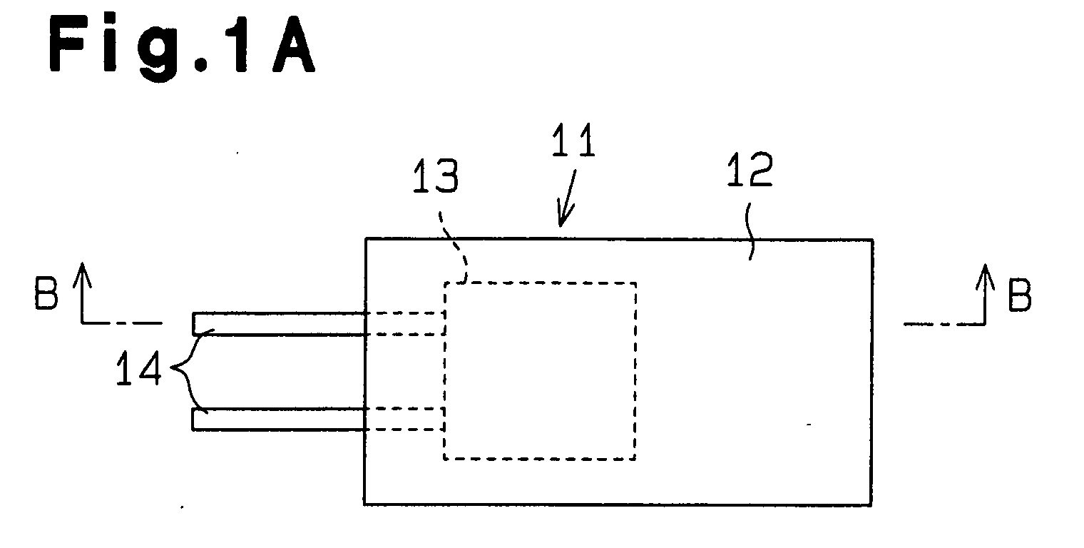
- a semiconductor device 11 includes a housing 12.
- the housing 12 is generally rectangular solid in shape and formed of thermoplastic resin.
- the housing 12 is formed of polyamide (PA).
- PA polyamide
- a semiconductor package 13 is sealed in the housing 12.
- the package 13 is generally rectangular solid in shape and formed of thermosetting epoxy resin.
- the surface 13a of the package 13 is modified by UV irradiation. Specifically, the modified face 13a of the package 13 has adhesive properties to the polyamide.
- a plurality (two in this embodiment) of connector terminals 14 extend from the package 13 in parallel. Each terminal 14 extends out of the housing 12 with one end of each terminal being sealed in the housing 12 together with the package 13.
- the package 13 is formed of thermosetting epoxy resin by a conventional method.
- the overall surface of the package 13 is irradiated by ultraviolet rays. This modifies the surface of the package 13 to be adhesive to polyamide.
- the package 13 is then placed in a die 20.
- the die 20 includes an upper die 20a and a lower die 20b.
- the dies 20a, 20b have a cavity that faces to each other so that a space 15 is defined in the die 20 when the dies 20a, 20b are positioned properly.
- the dies 20a, 20b have a semicylindrical recess at their opposing end.
- the two recesses forms cylindrical holes 20c.
- the internal diameter of the holes 20c is designed to be approximately the same as the external diameter of the terminals 14.
- thermoplastic resin PA in this embodiment
- PA melted thermoplastic resin
- the housing 12 is insert molded.
- the temperature at which the thermoplastic resin melts is lower than or the same as the temperature at which IC chips (not shown) in the package 13 shows heat resistance.
- the upper and lower dies 20a, 20b are opened.
- the housing 12 is formed with the package 13 and a part of the terminals 14 sealed. The semiconductor device 11 is completed.
- the semiconductor device 11 can be manufactured in one step by insert molding.
- conventionally required steps a step of performing a housing only, a step of adhering the package to the housing, and a step of filling the housing with the sealant, are abbreviated.
- the number of manufacturing steps is reduced and the semiconductor device 11 can be easily and inexpensively produced.
- the surface of the package 13 is UV-irradiated and modified to have adhesive properties to polyamide.
- the modified face 13a ensures the adhesiveness between the housing 12 and the package 13. Thus, and invasion of moisture from the gap between the terminal 14 and the housing 12 is prevented (and the integrity of the semiconductor device 11 is maintained). Thus, conventional problems, such as leaks or shorts, are avoided.
- a single polyamide is used as a thermoplastic resin. This improves the adhesive properties between the package 13 and the housing 12 compared with those when a polymer alloy of polyamide and another resin is used.
- the thermoplastic resin that forms the housing 12 is not limited to single PA.
- a resin of polymer alloy of PA and PPS polyphenylene sulfide
- the combination of PPS with PA improves heat resistance, dimensional stability, and low water absorption rate of the semiconductor device 11 compared with single PA, while keeping the adhesive properties between the package 13 and the housing 12.
- a resin of polymer alloy of PA and PBT may also be used.
- the combination of PBT with PA improves low water absorption rate and abrasion resistance compared with single PA.
- the terminal 14 may be a male connector.
- the number of the terminal 14 is not limited to two but may be one or more than two.
- the shape of the housing 12 and the package 13 is not limited to generally rectangular solid but may be varied in any suitable form.
Landscapes
- Structures Or Materials For Encapsulating Or Coating Semiconductor Devices Or Solid State Devices (AREA)
- Encapsulation Of And Coatings For Semiconductor Or Solid State Devices (AREA)
- Injection Moulding Of Plastics Or The Like (AREA)
- Treatments Of Macromolecular Shaped Articles (AREA)
Abstract
Description
Claims (9)
- A semiconductor device comprising a housing (12) formed of a first synthetic resin that is a thermoplastic resin and a semiconductor package (13) formed of a second synthetic resin that is a thermosetting resin, the package (13) being sealed in the housing (12), characterized by
a modified face (13a) that has adhesive properties to the first synthetic resin, wherein the modified face (13a) is formed on a surface of the package (13) by UV-irradiating the surface before the sealing of the package (13) in the housing (12). - A semiconductor device according to Claim 1, characterized in that the package (13) is sealed in the housing (12) by insert molding.
- A semiconductor device according to Claim 1, characterized in that the first synthetic resin comprises polyamide or a thermoplastic resin including polyamide.
- A semiconductor device according to Claim 3, characterized in that the second synthetic resin comprises a thermosetting epoxy resin.
- A semiconductor device according to Claim 3, characterized in that the thermoplastic resin is a polymer alloy of polyamide and polyphenylene sulfide.
- A semiconductor device according to Claim 3, characterized in that the thermoplastic resin is a polymer alloy of polyamide and polybutylene telephthalate.
- A method of making a semiconductor device comprising:UV-irradiating a semiconductor package (13) formed of thermosetting epoxy resin to modify its surface to be adhesive to polyamide;placing the package (13) in a die (20); andfilling a space (15) in the die (20) with melted polyamide or a melted thermoplastic resin including polyamide to seal the package (13) by insert molding.
- A method according to Claim 7, characterized in that the thermoplastic resin is a polymer alloy of polyamide and polyphenylene sulfide.
- A method according to Claim 7, characterized in that the thermoplastic resin is a polymer alloy of polyamide and polybutylene telephthalate.
Applications Claiming Priority (2)
| Application Number | Priority Date | Filing Date | Title |
|---|---|---|---|
| JP2001287076 | 2001-09-20 | ||
| JP2001287076A JP4620303B2 (en) | 2001-09-20 | 2001-09-20 | Semiconductor device and manufacturing method thereof |
Publications (2)
| Publication Number | Publication Date |
|---|---|
| EP1296371A2 true EP1296371A2 (en) | 2003-03-26 |
| EP1296371A3 EP1296371A3 (en) | 2006-05-24 |
Family
ID=19109943
Family Applications (1)
| Application Number | Title | Priority Date | Filing Date |
|---|---|---|---|
| EP02020768A Withdrawn EP1296371A3 (en) | 2001-09-20 | 2002-09-16 | Semiconductor device and method of making the same |
Country Status (3)
| Country | Link |
|---|---|
| US (2) | US20030052396A1 (en) |
| EP (1) | EP1296371A3 (en) |
| JP (1) | JP4620303B2 (en) |
Cited By (1)
| Publication number | Priority date | Publication date | Assignee | Title |
|---|---|---|---|---|
| US7588962B2 (en) | 2001-09-20 | 2009-09-15 | Kabushiki Kaisha Tokai Rika Denki Seisakusho | Method of making semiconductor device |
Families Citing this family (6)
| Publication number | Priority date | Publication date | Assignee | Title |
|---|---|---|---|---|
| DE102007051870A1 (en) * | 2007-10-30 | 2009-05-07 | Robert Bosch Gmbh | Module housing and method for producing a module housing |
| JP2010071724A (en) * | 2008-09-17 | 2010-04-02 | Mitsubishi Electric Corp | Resin molded semiconductor sensor and method of manufacturing the same |
| JP5038273B2 (en) * | 2008-09-17 | 2012-10-03 | 三菱電機株式会社 | Resin molded semiconductor sensor and manufacturing method |
| US9789637B2 (en) * | 2012-07-16 | 2017-10-17 | Denso Corporation | Electronic device and method for manufacturing the same |
| JP5983700B2 (en) | 2013-12-09 | 2016-09-06 | 株式会社デンソー | Semiconductor device, method for manufacturing the same, and composite molded body |
| WO2015129237A1 (en) | 2014-02-27 | 2015-09-03 | 株式会社デンソー | Resin molded article, and manufacturing method for same |
Family Cites Families (27)
| Publication number | Priority date | Publication date | Assignee | Title |
|---|---|---|---|---|
| US3689311A (en) | 1970-11-06 | 1972-09-05 | Ler Son Co Inc | Method for external coating of cylindrical objects |
| JPS6331149A (en) * | 1986-07-25 | 1988-02-09 | Fujitsu Ltd | Semiconductor device |
| JPS63102246U (en) * | 1986-12-22 | 1988-07-02 | ||
| KR0157844B1 (en) * | 1988-07-15 | 1998-10-15 | 모리나카 마사미 | Resin-sealed semiconductor device and manufacturing method |
| JP2701072B2 (en) * | 1989-06-20 | 1998-01-21 | 東レ・ダウコーニング・シリコーン株式会社 | Resin-sealed optical coupling semiconductor device and method of manufacturing the same |
| JP2701045B2 (en) * | 1988-07-15 | 1998-01-21 | 東レ・ダウコーニング・シリコーン株式会社 | Resin-sealed semiconductor device and method of manufacturing the same |
| US5519177A (en) * | 1993-05-19 | 1996-05-21 | Ibiden Co., Ltd. | Adhesives, adhesive layers for electroless plating and printed circuit boards |
| US5641997A (en) * | 1993-09-14 | 1997-06-24 | Kabushiki Kaisha Toshiba | Plastic-encapsulated semiconductor device |
| JPH07196898A (en) * | 1993-12-28 | 1995-08-01 | Kanebo Ltd | Thermoplastic resin composition |
| JPH0878582A (en) * | 1994-08-31 | 1996-03-22 | Toshiba Corp | Semiconductor device and semiconductor device manufacturing method |
| JP3176542B2 (en) * | 1995-10-25 | 2001-06-18 | シャープ株式会社 | Semiconductor device and manufacturing method thereof |
| DE69532651T2 (en) * | 1995-12-26 | 2004-07-29 | Ibiden Co. Ltd., Ogaki | METAL FILM COMPOSITE BODY, LINKING LAYER AND BINDING AGENT |
| US5786626A (en) * | 1996-03-25 | 1998-07-28 | Ibm Corporation | Thin radio frequency transponder with leadframe antenna structure |
| EP1271640A3 (en) * | 1996-07-12 | 2003-07-16 | Fujitsu Limited | Mold for manufacturing semiconductor device |
| JPH10212365A (en) * | 1996-11-29 | 1998-08-11 | Mitsui Chem Inc | Resin molding and its production |
| JPH1135915A (en) * | 1997-07-15 | 1999-02-09 | Toray Ind Inc | Resin-sealed semiconductor device |
| JPH11254477A (en) * | 1998-03-13 | 1999-09-21 | Mitsubishi Eng Plast Corp | Method for manufacturing resin-encapsulated molded products of electric and electronic parts |
| JPH11254476A (en) * | 1998-03-13 | 1999-09-21 | Mitsubishi Eng Plast Corp | Method for manufacturing resin-encapsulated molded products of electric and electronic parts |
| EP1114719B1 (en) * | 1999-02-22 | 2008-03-05 | Sekisui Chemical Co., Ltd. | Composite material and synthetic sleeper using the composite material |
| US6274927B1 (en) * | 1999-06-03 | 2001-08-14 | Amkor Technology, Inc. | Plastic package for an optical integrated circuit device and method of making |
| JP2001168117A (en) * | 1999-12-06 | 2001-06-22 | Idemitsu Petrochem Co Ltd | Release film for sealing semiconductor element and method for sealing semiconductor element using the same |
| JP3721935B2 (en) * | 2000-04-19 | 2005-11-30 | 住友電気工業株式会社 | Optical device |
| US6643919B1 (en) * | 2000-05-19 | 2003-11-11 | Siliconware Precision Industries Co., Ltd. | Method of fabricating a semiconductor device package having a core-hollowed portion without causing resin flash on lead frame |
| JP3534042B2 (en) * | 2000-06-21 | 2004-06-07 | オムロン株式会社 | Coin-shaped IC tag and method of manufacturing the same |
| JP4134499B2 (en) * | 2000-08-07 | 2008-08-20 | 住友電気工業株式会社 | Optical device |
| US7166910B2 (en) * | 2000-11-28 | 2007-01-23 | Knowles Electronics Llc | Miniature silicon condenser microphone |
| JP4620303B2 (en) | 2001-09-20 | 2011-01-26 | 株式会社東海理化電機製作所 | Semiconductor device and manufacturing method thereof |
-
2001
- 2001-09-20 JP JP2001287076A patent/JP4620303B2/en not_active Expired - Fee Related
-
2002
- 2002-09-16 EP EP02020768A patent/EP1296371A3/en not_active Withdrawn
- 2002-09-18 US US10/246,126 patent/US20030052396A1/en not_active Abandoned
-
2008
- 2008-09-04 US US12/204,502 patent/US7588962B2/en not_active Expired - Fee Related
Cited By (1)
| Publication number | Priority date | Publication date | Assignee | Title |
|---|---|---|---|---|
| US7588962B2 (en) | 2001-09-20 | 2009-09-15 | Kabushiki Kaisha Tokai Rika Denki Seisakusho | Method of making semiconductor device |
Also Published As
| Publication number | Publication date |
|---|---|
| EP1296371A3 (en) | 2006-05-24 |
| JP4620303B2 (en) | 2011-01-26 |
| JP2003094479A (en) | 2003-04-03 |
| US20030052396A1 (en) | 2003-03-20 |
| US7588962B2 (en) | 2009-09-15 |
| US20090023253A1 (en) | 2009-01-22 |
Similar Documents
| Publication | Publication Date | Title |
|---|---|---|
| US7588962B2 (en) | Method of making semiconductor device | |
| US6605331B1 (en) | Asymmetric transfer molding method and an asymmetric encapsulation made therefrom | |
| KR100870601B1 (en) | An ic card and method of manufacturing the same | |
| EP0747942B1 (en) | Improvements in or relating to integrated circuits | |
| US4816426A (en) | Process for manufacturing plastic pin grid arrays and the product produced thereby | |
| CN102569616B (en) | Semiconductor light emitting device packaging method and molded semiconductor light emitting device strip | |
| US20060162156A1 (en) | Method for making memory cards and similar devices using isotropic thermoset materials with high quality exterior surfaces | |
| US7667976B2 (en) | Electronic circuit device and method of making the same | |
| KR19980068001A (en) | Manufacturing method of semiconductor package | |
| JP2000326359A (en) | Composite integrally molded product using pre-molded member | |
| EP0807973A2 (en) | Plastic molded type semiconductor device and method of manufacturing the same | |
| US6472251B1 (en) | Method for integrated circuit packaging | |
| US6696006B2 (en) | Mold for flashless injection molding to encapsulate an integrated circuit chip | |
| US20160082631A1 (en) | Mold for Manufacturing LED Mounting Substrate | |
| JP2014175363A (en) | Manufacturing method of resin sealing module and resin sealing module | |
| US6737947B1 (en) | Assembly for sealing electrical leads to internal electrical device | |
| US20030080404A1 (en) | Semiconductor device and manufacturing method thereof | |
| US6177040B1 (en) | Method for making light transparent package for integrated circuit | |
| US8689438B2 (en) | Seal apparatus and method of manufacturing the same | |
| JP4809717B2 (en) | Method for manufacturing resin-encapsulated electronic component and resin-encapsulated electronic component | |
| CN119170529A (en) | Terminal packaging jig and power module packaging method | |
| US20250210479A1 (en) | Methods for battery connection in microelectronic packages | |
| JP2005081695A (en) | Resin molding mold | |
| JPH06244352A (en) | Lead frame and manufacturing method for semiconductor device | |
| KR900001116B1 (en) | Process for producing protective envelopes in which corresponding electric-electronic circuit component are dipped |
Legal Events
| Date | Code | Title | Description |
|---|---|---|---|
| PUAI | Public reference made under article 153(3) epc to a published international application that has entered the european phase |
Free format text: ORIGINAL CODE: 0009012 |
|
| AK | Designated contracting states |
Kind code of ref document: A2 Designated state(s): AT BE BG CH CY CZ DE DK EE ES FI FR GB GR IE IT LI LU MC NL PT SE SK TR Designated state(s): AT BE BG CH CY CZ DE DK EE ES FI FR GB GR IE IT LI LU MC NL PT SE SK TR |
|
| AX | Request for extension of the european patent |
Extension state: AL LT LV MK RO SI |
|
| PUAL | Search report despatched |
Free format text: ORIGINAL CODE: 0009013 |
|
| AK | Designated contracting states |
Kind code of ref document: A3 Designated state(s): AT BE BG CH CY CZ DE DK EE ES FI FR GB GR IE IT LI LU MC NL PT SE SK TR |
|
| AX | Request for extension of the european patent |
Extension state: AL LT LV MK RO SI |
|
| STAA | Information on the status of an ep patent application or granted ep patent |
Free format text: STATUS: THE APPLICATION IS DEEMED TO BE WITHDRAWN |
|
| 18D | Application deemed to be withdrawn |
Effective date: 20060401 |