EP1293790B1 - Appareil de test par balayage utilisant le suréchantillonage pour se synchroniser - Google Patents
Appareil de test par balayage utilisant le suréchantillonage pour se synchroniser Download PDFInfo
- Publication number
- EP1293790B1 EP1293790B1 EP01307925A EP01307925A EP1293790B1 EP 1293790 B1 EP1293790 B1 EP 1293790B1 EP 01307925 A EP01307925 A EP 01307925A EP 01307925 A EP01307925 A EP 01307925A EP 1293790 B1 EP1293790 B1 EP 1293790B1
- Authority
- EP
- European Patent Office
- Prior art keywords
- data
- host
- clock signal
- target
- test
- Prior art date
- Legal status (The legal status is an assumption and is not a legal conclusion. Google has not performed a legal analysis and makes no representation as to the accuracy of the status listed.)
- Expired - Lifetime
Links
- 238000012360 testing method Methods 0.000 title claims description 124
- 230000003111 delayed effect Effects 0.000 claims description 3
- 230000007704 transition Effects 0.000 description 13
- 238000004891 communication Methods 0.000 description 11
- 230000001960 triggered effect Effects 0.000 description 11
- 230000000630 rising effect Effects 0.000 description 10
- 230000005540 biological transmission Effects 0.000 description 8
- 238000012986 modification Methods 0.000 description 6
- 230000004048 modification Effects 0.000 description 6
- 230000000694 effects Effects 0.000 description 5
- 230000004044 response Effects 0.000 description 5
- 238000010586 diagram Methods 0.000 description 4
- 230000006870 function Effects 0.000 description 4
- 238000011084 recovery Methods 0.000 description 4
- 230000001360 synchronised effect Effects 0.000 description 4
- 238000013461 design Methods 0.000 description 3
- 238000012546 transfer Methods 0.000 description 3
- 238000004458 analytical method Methods 0.000 description 2
- 230000008859 change Effects 0.000 description 2
- 230000003750 conditioning effect Effects 0.000 description 2
- 230000001934 delay Effects 0.000 description 2
- 238000002405 diagnostic procedure Methods 0.000 description 2
- 238000003780 insertion Methods 0.000 description 2
- 230000037431 insertion Effects 0.000 description 2
- 238000000034 method Methods 0.000 description 2
- 238000012544 monitoring process Methods 0.000 description 2
- 238000005070 sampling Methods 0.000 description 2
- 230000003044 adaptive effect Effects 0.000 description 1
- 238000013459 approach Methods 0.000 description 1
- 230000008901 benefit Effects 0.000 description 1
- 239000000872 buffer Substances 0.000 description 1
- 239000003795 chemical substances by application Substances 0.000 description 1
- 230000009977 dual effect Effects 0.000 description 1
- 238000003708 edge detection Methods 0.000 description 1
- 238000011156 evaluation Methods 0.000 description 1
- 230000007246 mechanism Effects 0.000 description 1
- 230000009467 reduction Effects 0.000 description 1
- 230000002123 temporal effect Effects 0.000 description 1
Images


Classifications
-
- G—PHYSICS
- G01—MEASURING; TESTING
- G01R—MEASURING ELECTRIC VARIABLES; MEASURING MAGNETIC VARIABLES
- G01R31/00—Arrangements for testing electric properties; Arrangements for locating electric faults; Arrangements for electrical testing characterised by what is being tested not provided for elsewhere
- G01R31/28—Testing of electronic circuits, e.g. by signal tracer
- G01R31/317—Testing of digital circuits
- G01R31/3181—Functional testing
- G01R31/3185—Reconfiguring for testing, e.g. LSSD, partitioning
- G01R31/318533—Reconfiguring for testing, e.g. LSSD, partitioning using scanning techniques, e.g. LSSD, Boundary Scan, JTAG
- G01R31/318552—Clock circuits details
-
- G—PHYSICS
- G01—MEASURING; TESTING
- G01R—MEASURING ELECTRIC VARIABLES; MEASURING MAGNETIC VARIABLES
- G01R31/00—Arrangements for testing electric properties; Arrangements for locating electric faults; Arrangements for electrical testing characterised by what is being tested not provided for elsewhere
- G01R31/28—Testing of electronic circuits, e.g. by signal tracer
- G01R31/317—Testing of digital circuits
- G01R31/3181—Functional testing
- G01R31/319—Tester hardware, i.e. output processing circuits
- G01R31/3193—Tester hardware, i.e. output processing circuits with comparison between actual response and known fault free response
- G01R31/31937—Timing aspects, e.g. measuring propagation delay
Definitions
- the present invention relates to a system comprising a host, a target and connection means therebetween.
- a host a target
- connection means therebetween.
- one of the host and target may be an integrated circuit and the other of the host and target may be external to the integrated circuit.
- FIG. 1 shows a host 2 and a target 4.
- the host 2 sends data to the target 4 via a connection line 6.
- the target sends data to the host via a connection line 8.
- the target comprises a test access port (TAP) controller on an integrated circuit and the host is an off-chip counterpart to the TAP controller.
- TAP test access port
- One problem is that a significant length of cable, for example of the order of 0.5 metres may be provided between the host and the target.
- the connection between the host and the target may include signal conditioning logic such as buffers, line drivers, signal voltage level converters or the like. This means that this signal conditioning logic adds a path delay for each signal transition both for signals from the host to the target and from the target to the host.
- the host 2 has a first flip flop 10.
- This flip flop 10 receives two inputs 12 and 14.
- the first input 12 is a test data input TDI and comprises the data which is to be transmitted to the target 4.
- the second input 14 is a clock signal TCK which controls the clocking out of the test data TDI.
- the clock signal TCK is also transmitted to the target 4 via a separate connection or transmission path 5.
- the target 16 there is a flip flop 16 which receives the received test data TDI' from the host at one input 18 and the received clock signal TCK' at a second input 20.
- the received test data TDI' is the same as the test data transmitted by the host but with a delay resulting from the transmission of the data across the transmission path.
- the received clock signal TCK' is likewise the same as the clock signal TCK transmitted by the host but with a delay resulting form the transmission of the clock signal across the transmission path.
- the received test data TDI' is thus clocked in using the received clock signal TCK'.
- the received clock signal TCK' provides an input 22 to a second flip flop 24.
- the received clock signal TCK' is first passed through an inverter 23.
- a second input to the flip flop 24 is provided by a test data output TDO signal which comprises the data which is to be transmitted to the host. Accordingly, the received clock signal TCK' in the form of its inverse, at the target, is also used to clock the data out to the host.
- the host has a second flip flop 28 which receives the test data TDO' from the target and also the clock signal TCK generated by the host via input 32.
- the received test data TDO' is the same as the transmitted test data TDO but with a delay resulting from the transmission of the test data across path 8.
- the test data TDO' received from the target is thus clocked out with the clock signal TCK generated by the host.
- FIG. 3 shows the timing of the various signals.
- the first signal TCK represents the clock signal timing at the host.
- the second signal TCK' represents the clock signal timing at the target, the difference in timing between the two signals being due to the delay path between the host 2 and the target 4.
- TDI represents the timing of the data transmitted from the host whilst TDI' represents the timing of the data received at the target.
- the test data TDI transmitted by the host is clocked out by the host clock signal TCK whilst the test data TDI' received at the target is clocked in by the received clock signal TCK'.
- the received clock signal TCK' at the target is also used to clock out the test data TDO which is transmitted from the target 4 to the host 2.
- any transition in the data from the target to the host will arrive back at the host at least two path delay times (i.e. caused by the cabling between the host and the target and the target and the host) after the significant clock transition of the clock.
- These two path delays are also known as the loop delay.
- the clocking frequency of the clock signal has been limited to the inverse of the loop delay. In some implementations, depending on which and how many clock edges are used in a clock cycle, this could lead to a maximum clock frequency of half of the inverse of the loop delay.
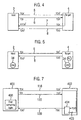
- the first solution is shown in Figure 4.
- the arrangement shown in Figure 4 works in a similar manner to that shown in Figure 2 except that the clock signal TCK' which is received by the target is then transmitted back to the host via connection 7.
- the returned clock signal RTCK is used to clock in at the host the data from the target.
- this solution is undesirable in that an additional pin connection is required with corresponding cabling. Additional pins are generally undesirable since the use of pins is generally at a premium.
- a further disadvantage with the arrangement shown in Figure 4 is that resynchronisation between the data from the target and the original clock signal is required in the host.
- FIG. 5 Another proposed solution to the problem with the arrangement of Figure 2 is shown in Figure 5.
- the host 2 and the target 4 each have an oscillator 34.
- the oscillator at the host is used to control the clocking of the data from the host to the target whilst the oscillator 34 is used to control the clocking of the data from the target to the host.
- Mechanisms such as phase locked loops may be provided in one or other or both of the host or target to try to achieve synchronisation.
- European Patent Application EP-A-1058121 relates to a method and apparatus for adaptive clocking for boundaries scan testing and device programming.
- An output clock is generated for use in shifting output data to a target device.
- a second clock is generated for receiving input data from a target device.
- the input clock is generated after the output clock according to a predetermined delay, thereby providing a period of time for the target device to respond to the serial stream of output data.
- United States Patent No. US-A-5689533 relates to a circuit for refined timing recovery comprising a data pulse edge detector.
- a recovered data signal is derived from a received data pulse.
- the pulse edge detector is adapted to sense the next clock pulse edge having the closest temporal proximity after a selected received data pulse edge.
- the output from the refined timing recovery circuit is a retiming edge signal used to retime recovered data signals.
- a receiver of n-bit data words each consisting of K information bits and (n-1) redundancy bits comprises three error detectors receiving the incoming bit stream in parallel with one another and with a shift register of a transfer circuit, the three error detectors being triggered by timing pulses fed to them in staggered relationship from a clock circuit extracting synchronising signals from the bit stream.
- a system comprising a host, a target and connection means therebetween, said host having means for providing a test clock signal, second output means for outputting data to said target via said connection means, said data being clocked out by said test clock signal, said target having second input means for receiving said data from said host and first output means for outputting data to said host via said connection means, said host further comprising input means for receiving said data from said target, said system characterised by; said host having first output means for outputting said test clock signal to said target via said connection means; said target having first input means for receiving said test clock signal from said host; said target is arranged to clock out data to said host over said first output means using said test clock signal and said host further comprising oversampling means for oversampling the received data from the target and controlling the clocking in of said data received from said target using said test clock signal in dependence on said oversampling.
- Figure 6 shows, in schematic form, the interconnection between a data adaptor 90 with on-chip destination/source logic such as a target CPU 162, and a host CPU 200.
- the integrated circuit 50 comprises a TAP controller 56, a data adaptor 90, a target CPU 162 including CPU registers 163 and an on-chip memory 164. Additionally, the integrated circuit of Figure 6 comprises diagnostic facilities 300 including diagnostic registers 301, a memory cache 302, an external memory interface controller 304, and a message converter 160.
- the host CPU 200 interfaces with the TAP controller 56 of the integrated circuit via a host communications adaptor 308.
- the host communications adaptor 308 includes a TAP controller initialiser, a data adaptor and a memory bus adaptor.
- the host communications adaptor 308 includes a message converter equivalent to the message converter 160 provided on the integrated circuit 50 for converting messages to and from the host CPU 200.
- the host CPU 200 and the host communications adaptor 308 are connected together via bus 306.
- the data adaptor 90 communicates with the diagnostic facilities 300, via message converter 160 and the diagnostic bus 234.
- the diagnostic facilities 300 and target CPU 162 communicate with each other via a bus 310.
- the memory monitor bus 226 and memory slave bus 220 of the message converter 160 are both connected to a common bus 312 between the target CPU 162 and the memory cache 302. Additionally, the target CPU 162 and memory cache 302 are interconnected via a CPU instruction fetch bus 314.
- the memory master bus 222 of the message converter 160 is connected to the memory cache 302, which in turn is connected to the memory bus 166 of the on-chip destination/source logic.
- the memory bus 166 is connected to the on-chip memory 164. Additionally, the memory bus 166 is connected to the external memory interface controller 304, which interfaces the on-chip destination/source logic memory bus 166 to an off-chip memory bus 316 which interfaces with off-chip memory 174.
- the structure of Figure 6 can be used to implement various diagnostic procedures by transmitting messages between the on-chip destination/source logic and the host CPU 200.
- the diagnostic bus 234 allows reading from and writing to the diagnostic registers 301 of the diagnostic facilities 300 and also allows triggered events to be read.
- Control information associated with the target CPU 162 is read from the diagnostic facilities 300.
- the instruction pointer and other control signals associated with the target CPU are stored in the diagnostic register 301 of the diagnostic facilities 300.
- the instruction pointer is continually copied into one of the diagnostic registers 301, and can be accessed by a request on the diagnostic bus 234. To look at the status of the target CPU, it is necessary to look at one of the diagnostic registers 301 of the diagnostic facilities 300.
- the diagnostic registers 301 can store various control signals of the target CPU 162, for example STORE, TRAP, TAKE A TRAP, TRAP AT NEXT INSTRUCTION. These signals are communicated to the CPU via specific wires.
- the host CPU may write to registers within the diagnostic facilities 300 via the diagnostic bus 234, in the same manner as the host CPU may write to memory locations within the target CPU memory space via the memory master bus 222 as discussed hereinabove.
- triggered events may occur. Such triggered events are detected in the message converter 160 by identifying a request signal associated with the reason code identifying the triggered event. In response to the request signal the message converter 160 loads the reason code associated with the triggered event together with the two bits identifying a triggered header byte. The triggered header byte is then output on the transmit data bus TX data to the target CPU.
- the target CPU can itself access the diagnostic facilities 300 via the memory monitor bus 226 and the diagnostic bus 234. Similarly, if the target CPU writes to the diagnostic facilities, and in response to such a write a triggered event occurs, then the message converter 160 will output the triggered header byte contained in the header register 240 back to the target CPU.
- a state machine 252 stores whether a write on the diagnostic bus 234 has been made by the target CPU or the host CPU and returns a triggered event to the correct destination accordingly.
- the data adaptor 90 enables serial data received from the TAP controller 52 to be transmitted in the direction of on-chip functional circuitry as parallel data and control signals.
- the data adaptor 90 supports a variety of high level diagnostic features, including boot from test access ports, hot plug insertion, and host and target synchronisation.
- the data adaptor 90 is supplied with the DIAG CLK signal on line 38, which is generated off-chip and the SYS-CLK signal on line 113, which is generated on-chip by the clock generator 117.
- the message converter 160 which is described in detail in EP-A-0840218, provides for communication between a host CPU and on-chip destination/source logic via a restricted pin count. Such a converter may have access to a variety of on-chip resources. Some of these may be simply monitored, others may be controlled or both monitored and controlled. Monitoring of any resource is nonintrusive, and has no impact on the performance or latency of the functionality of the chip. This is ideal for diagnostic purposes.
- the message converter 160 performs the functions of interpretation of received message, the compilation of transmit messages, and the selection or direction of information to/from the on-chip destination/source logic.
- the message converter 160 operates independently of any of the on-chip functionality and is therefore nonintrusive, until or unless it is directed to perform some intrusive operation.
- the TAP controller 56 is a synchronous finite state machine defined by the IEEE standard 1149.1-1990. That IEEE standard defines test logic which can be included in an integrated circuit to provide standardised approaches to testing and interconnections between integrated circuits, testing the integrated circuit itself, and observing or modifying circuit activity during the integrated circuits normal operation.
- the TAP controller 56 is in a reset state, and all of its inputs and outputs are inactive.
- the test access port controller operates according to the definitions of that standard. In such a test mode the test access port controller 56 should be able to select at least one test mode of operation.
- One possible test mode is a scan test mode in which scan data is clocked into a scan chain on-chip and/or alternative resultant data is clocked out for checking.
- the TAP controller 56 can also operate in a diagnostic mode of operation for carrying out diagnostic procedures of source/destination logic on-chip.
- the TAP controller 56 whilst continuing to provide all normal functionality, additionally acts as a transport agent carrying full duplex, flow controlled, unbounded, serial data, although the TAP controller is unaware that this is the form of the data.
- scan test mode the TAP controller normally handles a single stream of data, without any flow control passing through a selected scan chain.
- the communication of diagnostic data may include memory access requests from host to target and target to host (reads and writes); status information of CPU registers; data read from host memory or target memory in response to a memory access request; status data for loading into CPU register; and information about memory addresses being accessed by the target CPU.
- the diagnostic mode may involve nonintrusive monitoring of data, or intrusive loading of data.
- the serial data shifted into the test access port is a unidirectional serial data stream which can be encoded in any desired means, for example, the start and stop bits to delineate data chunks.
- data shifted out via the test access port is a unidirectional serial data stream which can be encoded in any desired means, for example with start and stop bits to delineate data chunks. Normally the data shifted in and the data shifted out will be encoded in the same way.
- the input and output unidirectional data streams may be used simultaneously to allow full-duplex, bi-directional serial communications.
- the sequence of serial data bits could constitute a byte of information.
- the data adaptor 90 enables a variety of high level diagnostic features to be supported including boot from test access ports, hot plug insertion and host and target synchronisation.
- the integrated circuit 50 is connected to the host communications adaptor 308 via five serial connections. In particular, these five serial connections are with the TAP controller 56.
- the first connection 114 provides a test reset signal.
- the second connection 116 provides a test clock signal.
- the third connection 118 provides a test mode signal.
- the fourth connection 122 provides test data in information.
- the first four connections are from the host communications adaptor 308 to the TAP controller 56.
- the test reset signal and the test mode signal together are able to put the TAP controller into various modes.
- the fifth connection 120 is the test data out connection and is from the TAP controller 56 to the host communications adaptor 308.
- the data adaptor 90 receives as inputs from the TAP controller 56 two main signal groups.
- the first signal group received at this interface represents the TAP controller in diagnostic mode and includes the DIAG.CLOCK signal on line 38, the DIAGMODE signal on line 54, and the DIAGSCANIN signal on line 52.
- This group includes the output signal DIAGSCANOUT on line 36.
- the DIAG.CLOCK signal on line 38 is the reference clock signal for the timing of the all signals on the TAP controller interface and has a significant rising edge. This signal corresponds to and maybe directly connected from the incoming clock signal TCK.
- the DIAGMODE signal on line 54 indicates that the TAP controller is in the diagnostic mode.
- the DIAGSCANIN signal on line 52 represents serial input data which is valid when the DIAGMODE signal is asserted.
- the DIAGSCANOUT signal represents serial output data which is valid when the DIAGMODE signal is asserted.
- Data adaptor signals at the on-chip interface include a further two groups, namely receive stream data signals and transmit stream data signals.
- the data adaptor 90 outputs data RX.DATA to on-chip source/destination logic on a receive data bus 94 and receives data TX.DATA from on-chip source/destination logic on a transmit data bus 92. All of the signals on the interface are synchronous signals.
- the signals on lines 100 and 102 are the control signals which regulate the flow of data on bus 94.
- the signals on lines 96 and 98 regulate the flow of data on bus 92.
- the receive stream data signals associated with the transfer of data RX.DATA on line 94 include the RX.REQUEST signal on line 100 which when asserted indicates that data is valid and a sample is requested to be transferred, the RX.GRANT signal on line 102 which is a "default grant" signal and may be asserted or withdrawn independently of RX.REQUEST.
- RX.GRANT When RX.GRANT is asserted and if the RX.REQUEST signal is also asserted, the data will be committed for transfer. However, when the RX.GRANT signal is asserted but the RX.REQUEST signal is not asserted, the RX.GRANT signal indicates merely that the on-chip source/destination logic is ready to transmit data.
- the host 400 incorporates the host communications adaptor 308 and host CPU 200 shown in Figure 6.
- the target 402 incorporates the integrated circuit 50. For clarity, only three of the five connections between the host and target are shown.
- the reset signals 114 and test mode signal 118 have been omitted for clarity.
- the test clock TCK signal is transmitted from the host 400 to the target 402.
- the test clock TCK signal is used at the host 400 to clock out the test data via connection 122.
- the test clock TCK 'signal received at the target is also used to clock in the test data at the target side 402.
- the received test clock TCK' signal is input to a flip flop 404 along with a test data out TDO signal.
- the received test clock TCK' signal is passed through an invertor 405 and used to clock out the test data TDO out via connection 120.
- the test data out is received at the host with a delay caused by connection 120 and is referred to as TDO'.
- the host 400 has over sampling logic 406. As will be described hereinafter, the oversampling logic 406 is used to counter the effects of the delay loop between the host 400 and the target 402, without requiring a reduction in the clock frequency.
- FIG. 8 illustrates the principles behind embodiments of the present invention.
- the circuitry shown in Figure 8 is incorporated in the host 400.
- the test data out TDO' received via the connection 120 is input to first and second flip flops 408 and 410 respectively.
- the test clock TCK of the host is input as the timing control signal to the first flip flop 408.
- the test clock TCK is inverted by an inverter 412 and used as the control input to the second flip flop 410.
- the output of the first and second flip flops 408 and 410 are input to a multiplexer 414 which is controlled by oversampling logic 416.
- the oversampling logic 416 receives the test data output signal and makes a determination whether or not the test data output is best clocked out by the test clock signal or its inverse. Once the oversampling logic 416 has made its determination, the multiplexer 414 is controlled to select the output of the first flip flop 408 or the second flip flop 410 as its output.
- the oversampling logic can take any suitable format and examples of this will be described hereinafter.
- Figure 9 uses the same principles as shown in Figure 8.
- the first chain of flip flops comprises four flip flops 422 to 428.
- the input of the first flip flop 420 is provided by the received test data out TDO' signal.
- the output of the first flip 422 provides the input to the second flip flop 424, with the second flip flop 424 output providing the input to the third flip flop 426 and the output of the third flip flop 426 providing the input to the fourth flip flop 428.
- Each of these flip flops receives the test clock TCK input as its control input.
- the second chain of flip flops is constructed in the same way as the first chain of flip flops and also comprises four flip flops 430 to 436. These flip flops receive the inverse of the test clock TCK as their control input. An inverter 438 is provided to generate the inverse of the test clock signal.
- An edge detector 440 provides an oversampling logic function. The edge detector looks at the timing of the signal input to the second flip flops 424 and 432 of the respective first and second flip flop chains 418 and 420 from the respective preceding flip flop and the timing of the signal input to the third flip flops 426 and 434 of the respective first and second flip flop chains 418 and 420 from the respective preceding flip flop. It should be appreciated that in alternative embodiments of the present invention, other ones of the flip flops in the chain may be additionally or alternatively be considered.
- Figure 10 shows a test clock signal.
- a signal 2xTCK having twice the test clock frequency is considered.
- the test clock signal TCK is synchronised with the double test clock signal 2xTCK in that the rising edges at the beginning of the test clock signal TCK coincides with a rising edge of the double test clock signal 2xTCK.
- the signals are sampled at the rising and falling edges of the double rate test clock signal 2xTCK. In other words, for each cycle of the test clock, four samples are done using the double test clock.
- the first half of the first clock cycle of the 2xTCK signal is labelled A and the second half B.
- the first half of the second clock signal is labelled C and the second half D. This corresponds to one cycle of the clock signal TCK. This same notation is used to reference the clock cycles of the 2xTCK signal corresponding to the next clock cycles of the test clock signal TCK.
- the test data TDO' received at the host may have a transition sometime within a clock cycle of the test clock signal.
- Case 1 represents test data which has a transition during one part of a clock cycle and case 2 represents test data which has a transition during another part of the clock cycle.
- Case 1 can have a transition in a second part of A, in B or the first part of C.
- Case 2 can have a transition in the second part of C, D or the first part of A. It should be appreciated that the definition of the ranges of case 1 and 2 and is a matter of design choice and any other suitable definition can be used,
- sampling for the second case is illustrated and samples are taken at the same time as for the first sample.
- the result cannot be read with certainty whilst for the second and third samples the data can be validly read.
- the received data will either have transitions in the range defined by case 1 or by case 2. If the data is in the range defined by case 1, it can be seen that the falling edge of the test clock signal can be used to clock in the data validly as this occurs between parts B and C. If the system requires rising clock edges to clock in data then the inverse of the clock signal can be used. If the data is in the range defined by case 2, then the rising edge of the test clock TCK can be used to clock in data. If the system requires a falling clock edge to clock in data then the inverse of the clock signal TCK can be used.
- the procedure carried out by the edge detector determines if the data received TDO' falls into the category defined by the first case or into the category defined by the second case. This also means that the clock signal to be used can be determined. For example some systems may use the clock signal TCK and it inverse. The edge detector will determine which of these clock signals to use.
- the oversampling clock signal may be available for the clocking in of data, in which case the falling edge at the beginning of A or the rising edge at the beginning of D could be used to clock in data if falling into the case 1 category. Likewise the falling edge at the beginning of B or the rising edge at the beginning of C could be used to clock in data if falling into the case 2 category.
- the number of possible cases can be more than two.
- the output of the first chain of flip flops 418 is selected if the test clock TCK is more appropriate or the output of the second chain of flip flops 420 is selected if the inverse test clock TCKinv is more appropriate by a multiplexer 442.
- the multiplexer 442 is controlled by the edge detector to select the output of one or other of the two flip flop chains 418 and 420.
- the output of the second flip flop chain 420 is connected to the input of a further flip flop 444 which receives the test clock signal TCK as an input. This further flip flop 444 is to ensure that the two flip flop chains provide equal delay.
- the flip flop 444 compensates for the fact that the inverse of the clock signal TCKinv is used to control the second flip flop chain 420.
- the output of the multiplexer 442 is input to a further flip flop 446 which provides further timing control.
- Figure 11 shows a modification to the arrangement of Figure 9.
- the arrangement of Figure 11 is arranged to have two modes of operation. During the initial mode of operation, a determination is made as to whether the test data should be clocked out using the test clock signal TCK or its inverse TCKinv. Once it has been established which of the test clock and its inverse should be used, the arrangement enters a stable mode where the flip flop chains are bypassed.
- TCK test clock signal
- TCKinv the test clock signal
- the arrangement enters a stable mode where the flip flop chains are bypassed.
- both the first flip flop chain 418 and the second flip flop 420 chain have a multiplexer 448 and 450 respectively arranged between the third 426 and 434 and fourth 428 and 436 flip flops. It should be appreciated that in alternative embodiments of the present invention, these multiplexers may be arranged at the end of each chain. These multiplexers 448 and 450 receive a first input from the output of the respective third flip flop 426 and 434 and a second input of the test data output directly, which bypasses the first three flip flops of the respective chains. The multiplexers 448 and 450 are controlled by the edge detector 440.
- the edge detector is also connected to the inputs and outputs respectively of the second flip flops 440 of the respective chains as in Figure 9 but this has been omitted for clarity.
- the edge detection 440 works in the same way as described in relation to Figures 9 and 10.
- the multiplexers 448 and 450 are controlled to select the output of the third flip flop during the initial mode when it is being determined whether or not the test data is best clocked out by the clock signal TCK or its inverse TCKinv. Once this determination has been made, the multiplexers 448 and 450 are arranged to output the test data which bypasses the three flip flops. In this way, in the normal mode of operation, unnecessary delay can be avoided.
- the multiplexers 448 and 450 have their outputs connected to the fourth flip flops 428 and 436 of the respective first and second flip flop chains 418 and 420.
- the other components of the circuit of Figure 11 work in a similar way to that described in relation to Figure 9.
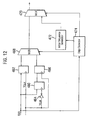
- Figure 12 shows a further modification to the arrangement shown in Figure 9.
- the arrangement comprises first and second flip flops 460 and 462.
- the first flip flop 462 receives the test data out TDO' as one input and the test clock signal TCK as another input.
- the second flip flop 460 receives the test data out TDO' as one input and the inverse of the test clock TCKinv as its second input.
- An inverter 464 is provided to invert the test clock signal.
- the second flip flop 460 is arranged in series with a third flip flop 466 which receives the output of the second flip flop 460 as one input and the clock signal TCK as a second input. This provides the same function as flip flop 444 described in relation to Figure 9.
- the output of the first and third flip flops 462 and 466 are input to a multiplexer which is controlled by an edge detector 474 in a similar manner to that described in the previous embodiments.
- the output of the first multiplexer 468 is input to a second multiplexer 470.
- the second multiplexer 470 has a second input from an initial sequence generator 472.
- the initial sequence generator 472 is controlled by the edge detector 474.
- the edge detector 474 analyses the test data signal in order to determine whether it is best clocked out by the test clock TCK or its inverse TCKinv.
- the edge detector 472 controls the second multiplexer 470 to either output the test data out received from the first multiplexer 468 or the output from the initial sequence generator.
- the initial sequence generator is arranged to output the test data which is used by the edge detector 472 to determine which clock signal to be used. In this way the initial data is not lost.
- the edge detector simply controls the second multtplexer to simply output the test data using the appropriate clock signal.
- at least one clock is generated which has the same clock frequency as the test clock frequency but is staggered with respect to the test clock. A plurality of evenly staggered clock signals can be generated in order to determine the most appropriate time to take a sample.
- the data is delayed by a number of steps.
- data having no delays is provided as is data having a delay n.
- the data having no delay or the data with delay n is then output in dependence in what is more appropriate for the test clock. In this way meta stable states can be avoided. More than two sets of data can be generated, each having a different delay.
- a signal having twice the clock frequency is used. It should be appreciated that in alternative embodiments of the present invention, other multiples of the clock frequency can be used.
- the clock or its inverse is selected. In alternative embodiments of the invention more than two options will be available. A separate flip flop chain may be provided for each option.
- Embodiments of the present invention have the advantage that no additional wires are required between the host and target. No changes to the on chip logic are required. Variations in the generation of the frequency of the clock signals at the host and target avoided.
- Embodiments of the present invention allow first order effects to be eliminated.
- First order effects are caused by the presence of the wire or any other type of connection.
- second order causes of variation in delay such as temperature change slowly. Accordingly, there is no need to continuously track for the best sample point which would impose bandwidth overhead. Occasional tracking is sufficient.
Landscapes
- Engineering & Computer Science (AREA)
- General Engineering & Computer Science (AREA)
- Physics & Mathematics (AREA)
- General Physics & Mathematics (AREA)
- Tests Of Electronic Circuits (AREA)
Claims (19)
- Système comprenant un hôte (400), une cible (402) et des moyens de connexion (116, 122, 120) entre eux, l'hôte comprenant des moyens pour fournir un signal d'horloge de test, des seconds moyens de sortie pour fournir des données à la cible par l'intermédiaire des moyens de connexion, les données étant cadencées en sortie par le signal d'horloge de test, la cible ayant des seconds moyens d'entrée pour recevoir des données à partir de l'hôte et des premiers moyens de sortie pour fournir des données à l'hôte par l'intermédiaire des moyens de connexion, l'hôte comprenant en outre des moyens d'entrée pour recevoir les données de la cible, le système étant caractérisé en ce que :l'hôte comporte des premiers moyens de sortie pour fournir le signal d'horloge de test à la cible par l'intermédiaire des moyens de connexion ;la cible comporte des premiers moyens d'entrée pour recevoir le signal d'horloge de test de l'hôte ;la cible est agencée pour cadencer la sortie de données vers l'hôte sur les premiers moyens de sortie en utilisant le signal d'horloge de test ; etl'hôte comprend en outre des moyens de suréchantillonnage (406) pour suréchantillonner les données reçues de la cible et commander le cadencement des données reçues de la cible en utilisant le signal d'horloge de test en dépendance avec le suréchantillonnage.
- Système selon la revendication 1, dans lequel le suréchantillonnage prend place à des intervalles de temps obtenus à partir du signal d'horloge de test.
- Système selon la revendication 1 ou 2, dans lequel les moyens de suréchantillonnage (406) sont agencés pour échantillonner les données en utilisant seulement le signal d'horloge de test et les données retardées de divers intervalles de temps.
- Système selon l'une quelconque des revendications précédentes, dans lequel les moyens de suréchantillonnage (406) sont agencés pour sélectionner l'un du signal d'horloge de test et de son inverse pour commander le cadencement en entrée des données.
- Système selon la revendication 1, 2 ou 4, dans lequel les moyens de suréchantillonnage (406) sont agencés pour produire un signal d'horloge ayant une fréquence supérieure à celle du signal d'horloge de test, les données étant suréchantillonnées en accord avec le signal d'horloge produit.
- Système selon la revendication 5, dans lequel la fréquence du signal d'horloge produit est deux fois celle du signal d'horloge de test.
- Système selon la revendication 1 ou 2, dans lequel les moyens de suréchantillonnage (406) sont agencés pour utiliser une pluralité de signaux d'horloge ayant la même fréquence pour suréchantillonner les données reçues, les signaux d'horloge étant échelonnés les uns par rapport aux autres.
- Système selon la revendication 7, dans lequel les signaux d'horloge sont décalés de façon régulière.
- Système selon la revendication 7 ou 8, dans lequel les signaux d'horloge ont la même fréquence que le signal d'horloge de test.
- Système selon l'une quelconque des revendications 1 à 3, dans lequel les moyens de suréchantillonnage (406) sont agencés pour fournir au moins une copie des données, ladite au moins une copie étant retardée par rapport auxdites données, les moyens de suréchantillonnage sélectionnant l'une desdites données et de ladite au moins une copie des données à faire entrer.
- Système selon la revendication 10, dans lequel les données sélectionnées sont cadencées en utilisant le signal d'horloge de test.
- Système selon l'une quelconque des revendications précédentes, dans lequel l'hôte (400) a un premier mode de fonctionnement et un second mode de fonctionnement, et dans lequel, dans le premier mode de fonctionnement, les moyens de suréchantillonnage (406) sont agencés pour déterminer comment les données reçues doivent être cadencées, et, dans le second mode de fonctionnement, les données sont cadencées comme cela est déterminé dans le premier mode.
- Système selon la revendication 12, dans lequel, dans le second mode, les données reçues sont au moins partiellement dérivées par rapport aux moyens de suréchantillonnage (406).
- Système selon l'une quelconque des revendications précédentes, dans lequel les moyens de suréchantillonnage (406) comprennent une pluralité de trajets de données (418, 420), des trajets différents amenant les données à être cadencées de diverses manières.
- Système selon la revendication 14, dans lequel les trajets de données (418, 420) comprennent une pluralité de bascules.
- Système selon l'une quelconque des revendications précédentes, dans lequel les données en provenance de l'hôte (400) sont cadencées en entrée vers la cible (402) par le signal d'horloge de test reçu.
- Système selon l'une quelconque des revendications précédentes, dans lequel les données en provenance de la cible (403) sont cadencées en sortie par le signal d'horloge de test reçu.
- Système selon l'une quelconque des revendications précédentes, dans lequel au moins l'un de la cible (402) et de l'hôte (400) comprend un circuit intégré.
- Système selon l'une quelconque des revendications précédentes, dans lequel au moins les données fournies par la cible (402) ou les données fournies par l'hôte (400) comprennent des données de test.
Priority Applications (3)
| Application Number | Priority Date | Filing Date | Title |
|---|---|---|---|
| DE60125360T DE60125360D1 (de) | 2001-09-18 | 2001-09-18 | Abfrageprüfgerät, das Überabtastung zur Synchronisierung verwendet |
| EP01307925A EP1293790B1 (fr) | 2001-09-18 | 2001-09-18 | Appareil de test par balayage utilisant le suréchantillonage pour se synchroniser |
| US10/247,263 US7489724B2 (en) | 2001-09-18 | 2002-09-18 | System and method for connecting a host and a target |
Applications Claiming Priority (1)
| Application Number | Priority Date | Filing Date | Title |
|---|---|---|---|
| EP01307925A EP1293790B1 (fr) | 2001-09-18 | 2001-09-18 | Appareil de test par balayage utilisant le suréchantillonage pour se synchroniser |
Publications (2)
| Publication Number | Publication Date |
|---|---|
| EP1293790A1 EP1293790A1 (fr) | 2003-03-19 |
| EP1293790B1 true EP1293790B1 (fr) | 2006-12-20 |
Family
ID=8182273
Family Applications (1)
| Application Number | Title | Priority Date | Filing Date |
|---|---|---|---|
| EP01307925A Expired - Lifetime EP1293790B1 (fr) | 2001-09-18 | 2001-09-18 | Appareil de test par balayage utilisant le suréchantillonage pour se synchroniser |
Country Status (3)
| Country | Link |
|---|---|
| US (1) | US7489724B2 (fr) |
| EP (1) | EP1293790B1 (fr) |
| DE (1) | DE60125360D1 (fr) |
Families Citing this family (7)
| Publication number | Priority date | Publication date | Assignee | Title |
|---|---|---|---|---|
| DE60323246D1 (de) * | 2003-12-17 | 2008-10-09 | St Microelectronics Res & Dev | TAP-Daten-Transfer mit doppelter Daten-Rate |
| US7071738B1 (en) * | 2004-06-24 | 2006-07-04 | Xilinx, Inc. | Glitchless clock selection circuit using phase detection switching |
| EP1912411B1 (fr) * | 2006-10-12 | 2010-03-31 | Koninklijke KPN N.V. | Méthode et système pour préparer de service d'un dispositif d'accès dans un réseau résidentiel |
| TW200835178A (en) * | 2007-02-02 | 2008-08-16 | Smedia Technology Corp | Multi-sampling data recovery circuit and method applicable to receiver |
| US7949917B2 (en) * | 2007-12-13 | 2011-05-24 | Texas Instruments Incorporated | Maintaining data coherency in multi-clock systems |
| JP2009147869A (ja) * | 2007-12-18 | 2009-07-02 | Ricoh Co Ltd | 同期化回路 |
| US8248105B2 (en) | 2010-02-16 | 2012-08-21 | Taiwan Semiconductor Manufacturing Company, Ltd. | Smart edge detector |
Citations (3)
| Publication number | Priority date | Publication date | Assignee | Title |
|---|---|---|---|---|
| US3938086A (en) * | 1974-04-11 | 1976-02-10 | Societa Italiana Telecomunicazioni Siemens S.P.A. | Circuit arrangement for correcting slip errors in pcm receivers |
| WO1995001021A1 (fr) * | 1993-06-25 | 1995-01-05 | Xircom, Incorporated | Extraction du signal d'horloge sans retour a zero a horloge instantanee |
| US5689533A (en) * | 1994-09-30 | 1997-11-18 | Lucent Technologies Inc. | Refined timing recovery circuit |
Family Cites Families (18)
| Publication number | Priority date | Publication date | Assignee | Title |
|---|---|---|---|---|
| US3974333A (en) * | 1975-09-24 | 1976-08-10 | Bell Telephone Laboratories, Incorporated | Adaptive synchronization system |
| FR2685594B1 (fr) * | 1991-12-19 | 1994-01-28 | Alcatel Telspace | Dispositif de recuperation de rythme pour installation de reception utilisant l'egalisation auto-adaptative a sur-echantillonnage associee a la demodulation differentiellement coherente. |
| US5714904A (en) * | 1994-06-06 | 1998-02-03 | Sun Microsystems, Inc. | High speed serial link for fully duplexed data communication |
| US5529068A (en) * | 1994-06-16 | 1996-06-25 | The Regents Of The University Of California | Synchronized digital signal processor for MRI reception |
| GB9622686D0 (en) | 1996-10-31 | 1997-01-08 | Sgs Thomson Microelectronics | A test port controller and a method of effecting communication using the same |
| GB9622685D0 (en) | 1996-10-31 | 1997-01-08 | Sgs Thomson Microelectronics | An integrated circuit device and method of communication therewith |
| US6154509A (en) * | 1998-01-16 | 2000-11-28 | Natural Microsystems Corp. | Data phase recovery system |
| US6047021A (en) * | 1998-04-16 | 2000-04-04 | Grimes; James E. | Methods and apparatus for exchanging data |
| GB9810512D0 (en) * | 1998-05-15 | 1998-07-15 | Sgs Thomson Microelectronics | Detecting communication errors across a chip boundary |
| US6463092B1 (en) * | 1998-09-10 | 2002-10-08 | Silicon Image, Inc. | System and method for sending and receiving data signals over a clock signal line |
| US6895062B1 (en) * | 1999-03-24 | 2005-05-17 | International Business Machines Corporation | High speed serial interface |
| GB9907254D0 (en) | 1999-03-29 | 1999-05-26 | Sgs Thomson Microelectronics | Synchronous data adaptor |
| US6651200B1 (en) * | 1999-06-04 | 2003-11-18 | Acculogic, Inc. | Method and apparatus for adaptive clocking for boundary scan testing and device programming |
| US6553087B1 (en) * | 2000-05-04 | 2003-04-22 | 2Wire, Inc. | Interpolating bandpass filter for packet-data receiver synchronization |
| US6714612B1 (en) * | 2000-06-08 | 2004-03-30 | Sun Microsystems, Inc. | Method and device for synchronization of phase mismatch in communication systems employing a common clock period |
| KR100346837B1 (ko) * | 2000-09-02 | 2002-08-03 | 삼성전자 주식회사 | 클럭 스큐에 의한 에러를 최소화하는 데이타 복원 장치 및그 방법 |
| US6907096B1 (en) * | 2000-09-29 | 2005-06-14 | Intel Corporation | Data recovery method and apparatus |
| US6704882B2 (en) * | 2001-01-22 | 2004-03-09 | Mayo Foundation For Medical Education And Research | Data bit-to-clock alignment circuit with first bit capture capability |
-
2001
- 2001-09-18 DE DE60125360T patent/DE60125360D1/de not_active Expired - Lifetime
- 2001-09-18 EP EP01307925A patent/EP1293790B1/fr not_active Expired - Lifetime
-
2002
- 2002-09-18 US US10/247,263 patent/US7489724B2/en active Active
Patent Citations (3)
| Publication number | Priority date | Publication date | Assignee | Title |
|---|---|---|---|---|
| US3938086A (en) * | 1974-04-11 | 1976-02-10 | Societa Italiana Telecomunicazioni Siemens S.P.A. | Circuit arrangement for correcting slip errors in pcm receivers |
| WO1995001021A1 (fr) * | 1993-06-25 | 1995-01-05 | Xircom, Incorporated | Extraction du signal d'horloge sans retour a zero a horloge instantanee |
| US5689533A (en) * | 1994-09-30 | 1997-11-18 | Lucent Technologies Inc. | Refined timing recovery circuit |
Also Published As
| Publication number | Publication date |
|---|---|
| US20030068000A1 (en) | 2003-04-10 |
| DE60125360D1 (de) | 2007-02-01 |
| EP1293790A1 (fr) | 2003-03-19 |
| US7489724B2 (en) | 2009-02-10 |
Similar Documents
| Publication | Publication Date | Title |
|---|---|---|
| EP0982595B1 (fr) | Circuit intégré ayant plusieurs processeurs | |
| US9739834B1 (en) | System and method for transferring serialized test result data from a system on a chip | |
| US8151151B2 (en) | Tap time division multiplexing with scan test | |
| US8046647B2 (en) | TAP sampling at double rate | |
| US4791653A (en) | Pseudorandom word sequence synchronizer | |
| EP1624635A2 (fr) | Dispositif et procédé de transmission sychrone de données en parallèle en employant un signal de référence | |
| JPS61146030A (ja) | データ流れ同期装置 | |
| US6928528B1 (en) | Guaranteed data synchronization | |
| US6526535B1 (en) | Synchronous data adaptor | |
| EP1293790B1 (fr) | Appareil de test par balayage utilisant le suréchantillonage pour se synchroniser | |
| CN110515879B (zh) | 一种异步传输装置及其传输方法 | |
| EP1544633B1 (fr) | Multiplexeur pour TAP | |
| US6085285A (en) | Intermixing different devices along a single data communication link by placing a strobe signal in a parity bit slot | |
| EP1544630B1 (fr) | Scan test avec multiplexage de TAP dépendant du temps | |
| US7020148B1 (en) | Data transferring apparatus and data transferring method that use fast ring connection | |
| CN114003543A (zh) | 一种高速串行总线时钟补偿方法及系统 |
Legal Events
| Date | Code | Title | Description |
|---|---|---|---|
| PUAI | Public reference made under article 153(3) epc to a published international application that has entered the european phase |
Free format text: ORIGINAL CODE: 0009012 |
|
| AK | Designated contracting states |
Kind code of ref document: A1 Designated state(s): AT BE CH CY DE DK ES FI FR GB GR IE IT LI LU MC NL PT SE TR Designated state(s): AT BE CH CY DE DK ES FI FR GB GR IE IT LI LU MC NL PT SE TR |
|
| AX | Request for extension of the european patent |
Extension state: AL LT LV MK RO SI |
|
| 17P | Request for examination filed |
Effective date: 20030919 |
|
| AKX | Designation fees paid |
Designated state(s): DE FR GB IT |
|
| 17Q | First examination report despatched |
Effective date: 20040826 |
|
| GRAP | Despatch of communication of intention to grant a patent |
Free format text: ORIGINAL CODE: EPIDOSNIGR1 |
|
| GRAS | Grant fee paid |
Free format text: ORIGINAL CODE: EPIDOSNIGR3 |
|
| GRAA | (expected) grant |
Free format text: ORIGINAL CODE: 0009210 |
|
| AK | Designated contracting states |
Kind code of ref document: B1 Designated state(s): DE FR GB IT |
|
| PG25 | Lapsed in a contracting state [announced via postgrant information from national office to epo] |
Ref country code: IT Free format text: LAPSE BECAUSE OF FAILURE TO SUBMIT A TRANSLATION OF THE DESCRIPTION OR TO PAY THE FEE WITHIN THE PRESCRIBED TIME-LIMIT;WARNING: LAPSES OF ITALIAN PATENTS WITH EFFECTIVE DATE BEFORE 2007 MAY HAVE OCCURRED AT ANY TIME BEFORE 2007. THE CORRECT EFFECTIVE DATE MAY BE DIFFERENT FROM THE ONE RECORDED. Effective date: 20061220 |
|
| REG | Reference to a national code |
Ref country code: GB Ref legal event code: FG4D |
|
| REF | Corresponds to: |
Ref document number: 60125360 Country of ref document: DE Date of ref document: 20070201 Kind code of ref document: P |
|
| PG25 | Lapsed in a contracting state [announced via postgrant information from national office to epo] |
Ref country code: DE Free format text: LAPSE BECAUSE OF FAILURE TO SUBMIT A TRANSLATION OF THE DESCRIPTION OR TO PAY THE FEE WITHIN THE PRESCRIBED TIME-LIMIT Effective date: 20070321 |
|
| ET | Fr: translation filed | ||
| PLBE | No opposition filed within time limit |
Free format text: ORIGINAL CODE: 0009261 |
|
| STAA | Information on the status of an ep patent application or granted ep patent |
Free format text: STATUS: NO OPPOSITION FILED WITHIN TIME LIMIT |
|
| 26N | No opposition filed |
Effective date: 20070921 |
|
| REG | Reference to a national code |
Ref country code: FR Ref legal event code: PLFP Year of fee payment: 16 |
|
| REG | Reference to a national code |
Ref country code: FR Ref legal event code: PLFP Year of fee payment: 17 |
|
| REG | Reference to a national code |
Ref country code: FR Ref legal event code: PLFP Year of fee payment: 18 |
|
| PGFP | Annual fee paid to national office [announced via postgrant information from national office to epo] |
Ref country code: FR Payment date: 20200819 Year of fee payment: 20 Ref country code: GB Payment date: 20200819 Year of fee payment: 20 |
|
| REG | Reference to a national code |
Ref country code: GB Ref legal event code: PE20 Expiry date: 20210917 |
|
| PG25 | Lapsed in a contracting state [announced via postgrant information from national office to epo] |
Ref country code: GB Free format text: LAPSE BECAUSE OF EXPIRATION OF PROTECTION Effective date: 20210917 |