EP1292839B1 - Automatisches gerät für testbarkeitsanalyse - Google Patents
Automatisches gerät für testbarkeitsanalyse Download PDFInfo
- Publication number
- EP1292839B1 EP1292839B1 EP01943583A EP01943583A EP1292839B1 EP 1292839 B1 EP1292839 B1 EP 1292839B1 EP 01943583 A EP01943583 A EP 01943583A EP 01943583 A EP01943583 A EP 01943583A EP 1292839 B1 EP1292839 B1 EP 1292839B1
- Authority
- EP
- European Patent Office
- Prior art keywords
- signal
- binary
- binary decision
- value
- state
- Prior art date
- Legal status (The legal status is an assumption and is not a legal conclusion. Google has not performed a legal analysis and makes no representation as to the accuracy of the status listed.)
- Expired - Lifetime
Links
Images

Classifications
-
- G—PHYSICS
- G01—MEASURING; TESTING
- G01R—MEASURING ELECTRIC VARIABLES; MEASURING MAGNETIC VARIABLES
- G01R31/00—Arrangements for testing electric properties; Arrangements for locating electric faults; Arrangements for electrical testing characterised by what is being tested not provided for elsewhere
- G01R31/28—Testing of electronic circuits, e.g. by signal tracer
- G01R31/317—Testing of digital circuits
- G01R31/3181—Functional testing
- G01R31/3183—Generation of test inputs, e.g. test vectors, patterns or sequences
- G01R31/318371—Methodologies therefor, e.g. algorithms, procedures
Definitions
- the field of application of the invention is that of automatic tools for analyzing testability and automatic generation of complex logic circuit tests.
- a design phase In an integrated circuit manufacturing process, a design phase, usually computer-assisted, generates a list of connectors (netlist in English).
- a list of connectors contains circuit elements such as transistors and input-output connectors as well as the links between these elements such as tracks for conveying signals from one element to another.
- the connector list makes it possible to generate a mask which is used to burn the circuit in a semiconductor material, so as to produce pellets (wafer in English) for each constitute a physical sample of the circuit.
- each sample is tested in applying electrical state stimuli to certain signals in the sample and observing whether the resulting electrical signal states are in accordance with those provided for in design phase of the circuit.
- Test vectors each representing a set of stimuli, are determined at means of a computer which processes in memory the list of connections of the circuit. Saw the complexity of the current integrated circuits, a comprehensive treatment of the list of connectors truth tables would require memory sizes and compute times incompatible with production constraints in terms of time and cost.
- a binary decision diagram T f associated with a first Boolean function f (a, b, c, ..., w) of binary variables a, b, c, ..., w, is accessible by means of a first computer data structure that makes it possible to represent in memory the values taken by the first function f according to the values taken by the binary variables a, b, c, ..., w.
- the second and third data structures are of the same type as the first data structure with respectively a second and a third node occupied by a second binary variable b, c.
- the above operation repeated until the last binary variable w gives the binary decision diagram T f consists of a sequence ⁇ a, ⁇ b, ⁇ ... ⁇ , ⁇ ... ⁇ , ⁇ b, ⁇ . .. ⁇ , ⁇ ... ⁇ structures using pointers.
- An identifier of the binary decision diagram T f points to the first node then called root node.
- the representation in memory of a function by a binary decision diagram has an appreciable advantage of compactness because, if two or more subdiagrams of binary decision are identical, only one representation in memory just two or more pointers that can point to the same data structure.
- the decision diagram binary simplifies itself.
- the representation in memory of a function by a binary decision diagram can be implicit in the sense that it is possible to do calculations on the root node without necessarily developing the diagram of binary decision for all nodes.
- the binary decision diagram associated with the logical complement of a function f therefore comprises the same node occupied by the variable a as the binary decision diagram associated with the function f where the pointer on the binary decision subdiagram associated with the function f for a equal to zero is replaced by a pointer on a binary decision sub-diagram associated with the logical complement of the function f for a equal to zero, and where the pointer on the binary decision subdiagram associated with the function f for a equal to one is replaced by a pointer to a binary decision subdiagram associated with the logical complement of the function f for a equal to one.
- the binary decision diagram associated with the logical disjunction of two functions f and g thus comprises the same node occupied by the variable a as the binary decision diagram associated with the function f where the pointer on the binary decision subdiagram associated with the function f for a equal to zero is replaced by a pointer on a binary decision sub-diagram associated with the logical disjunction of the function f for a equal to zero and of the function g for a equal to zero, and where the pointer on the binary decision subdiagram associated with the function f for a equal to one is replaced by a pointer on a binary decision sub-diagram associated with the logical disjunction of the function f for a equal to one and the function g for a equal to one.
- the binary decision diagram associated with the logical conjunction of two functions f and g therefore understands the same node occupied by the variable a as the decision diagram binary associated with the function f where the pointer on the binary decision subdiagram associated with the function f for a equal to zero is replaced by a pointer on a subdiagram of binary decision associated with the logical conjunction of the function f for a equal to zero and the function g for a equal to zero, and where the pointer on the subdiagram of binary decision associated with the function f for a equal to one is replaced by a pointer on a binary decision subdiagram associated with the logical conjunction of the function f for a equal to one and the function g for a equal to one.
- a signal can take more than two states, for example a logic high or low but also a state of high impedance output of transistor set to a blocked state or to an indeterminate state on a node of junction of several tracks carrying different signal states.
- the invention mitigates this disadvantage.
- a logical conjunction of the first and the second binary decision diagram which leads to the first value codes the first state of the signal.
- a logical conjunction of the first and the complement of the second binary decision diagram which leads to the first value code the second state of the signal.
- a logical conjunction of the complement of the first and the second binary decision diagram which leads to the first value code the third state of the signal.
- the invention also has for corollary objects a computer system, such as a computer, a computer program and a recording medium, such as a floppy disk magnetic or a CD-ROM, allowing the implementation of the method of the invention.
- a computer system such as a computer, a computer program and a recording medium, such as a floppy disk magnetic or a CD-ROM, allowing the implementation of the method of the invention.
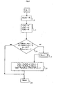
- Figure 1 depicts the steps of the method implemented by computer to a netlist of a monitored circuit, a signal s i is extracted.
- a pair of binary variables (x vi , x ci ) is assigned to the signal s i to encode three possible states of the signal s i .
- the variable x ci called the context variable, is defined to indicate that, when its value is equal to 1, the values 0 and 1 of the variable x vi respectively directly code logical states B and H of the signal s i .
- the values 0 and 1 of the variable x vi respectively code an indeterminate state and a state Z of the signal s i .
- the state Z of the signal s i is that of high impedance in the sense that is usually understood in an electrical circuit.
- a second step 2 three binary decision diagrams T v (s i ), T c (s i ), T e (s i ), are assigned to the signal s i .
- the binary decision diagram T v (s i ), referred to as value, is constructed so that it leads to 1 if the state of the signal s i is the state of high impedance Z or the logic state H .
- the binary decision diagram T c (s i ), referred to as context, is constructed so that it leads to 1 if the state of the signal si is the logic state B or the logic state H.
- the binary decision diagram T e (s i), said error is constructed so as to lead to 1 if the state of the signal s i is an error state.
- the computer searches in the connector list if there is an element generating the signal s i from one or more signals s i + 1 , s i + 2 .
- each of the variables x vi , x ci of the pair of binary variables (x vi , x ci ) can take a value equal to 0 or 1. It is for example the case for an input signal of the electric circuit or for an intermediate signal that can be forced by means of a test point.
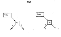
- the binary decision diagrams T v (s i ), T c (s i ) are represented in FIG. 2 where T v (s i ) leads to 1 if x vi is equal to 1, T c (s i ) leads to 1 if x ci is equal to 1.
- T e (s i ) has no reason to be because it would be detrimental to apply an error on an input of a circuit to be tested.
- the method then goes directly from step 3 to a return step 6 which makes the binary decision diagrams available in computer memory.
- the computer searches, in a library of rules, for one or more rules giving a behavior of the signal s i as a function of the signal or signals s i + 1 , s i + 2 for the element of the list of connections generating the signal s i .
- step 4 the binary decision diagrams T v (s i + 1 ), T c (s i + 1 ), T e (s i + 1 ) for each signal s i + 1 are searched in memory of the computer. If these binary decision diagrams do not already exist, steps 1 to 6 are executed recursively for each of the signals s i + 1 .
- a driver 21 carries a signal s 1 .
- the conductor 21 is connected at a point 25 to three conductors 22, 23, 24 in parallel.
- the conductors 22, 23, 24 respectively convey a signal s 2 , s 3 , s 4 respectively .
- the connection of the signals s 2, s 3 the point 25 is equivalent to an intermediate signal s 11 connected to point 25 with the signal s 4.
- the variable xv1 is equal to 1 if and only if the state of each of the signals s 1 , s 2 , s 3 is the state of high impedance Z or the logic state H.
- T v (s 11 ) T v (s 11 ) ⁇ T v (s 4 ).
- the variable xc1 is equal to 1 if the state of the signal s 1 is the state B or the logical state H.
- the signal s 11 is in the B or H state if and only if the signal s 2 or the signal s 3 is in the B or logic H state and if no error results from the signals s 2 and s 3 on the signal s 11 .
- the rule Rc applicable to construct the binary decision diagram T c (s 11 ) is a rule Rcr for two conductors connected to point 25:
- the second step is repeated for signal 2 .
- the conductor 22 is connected to the drain of a N-type MOS transistor 27.
- the gate of transistor 27 receives a signal s 5 and the source of transistor 27 receives a signal s 6 .
- the concept of drain and source of a transistor is related in known manner to its operating regime, so these two notions are interchangeable.
- the signal s 2 is in the logical H state if and only if the signals s 5 and s 6 are in the logical H state.
- the signal s 2 is in the high impedance state Z if and only if the signal s 5 is in the logic B state or if the signal s 5 is in the logic state H and the signal s 6 is in the Z state of high impedance.
- the rule Rv that applies is an Rvn rule: which for simplification gives:
- the signal s 2 is in the error state E if the signal s 5 is in the high impedance state Z. Indeed, a transistor gate driven by a high impedance signal is particularly sensitive to noise.
- the signal s 2 is in the B or logical H state if and only if the signal s 5 is in the logic H state and the signal s 6 is in the B or logic H state.
- the second step is repeated for the signal s 4 .
- the conductor 23 is connected to the drain of a N-type MOS transistor 26.
- the gate of transistor 26 receives a signal s 7 and the source of transistor 26 receives a signal s 8 .
- the first two steps are executed for the signal s 3 using the same rules Rvn, Rcn and Ren as for the signal s 2 so as to obtain:
- You ( s 3) Tv ( s 7) ⁇ Tc ( s 7)
- Tc ( s 3) Tc ( s 7) ⁇ TV ( s 7) ⁇ Tc ( s 8)
- the conductor 24 is connected to the drain of a P-type MOS transistor 29.
- the gate of transistor 29 receives a signal s 9 and the source of transistor 27 receives a signal s 10 .
- the signal s 4 is in the logical H state if and only if the signals s 9 and s 10 are respectively in the state B and logical H.
- the signal s 4 is in the high impedance state Z if and only if the signal s 9 is in the logic H state or if the signal s 9 is at the logic B state and the signal s 10 is at the Z state of high impedance.
- the Rv rule that applies is an Rvp rule:
- the signal s 4 is in the error state E if the signal s 9 is in the high impedance state Z. Indeed, a transistor gate driven by a high impedance signal is particularly sensitive to noise.
- the signal s 4 is in the B or logical H state if and only if the signal s 9 is in the logic B state and the signal s 10 is in the B or logic H state.
- the binary decision diagrams T v (s 1 ), T c (s 1 ), T e (s 1 ) are thus obtained as a function of the binary decision diagrams T v (s 5 ), T c (s 5 ), T v (s 6 ), T c (s 6 ), T v (s 7 ), T c (s 7 ), T v (s 8 ), T c (s 8 ), T v (s 9 ), T c (s 9 ), T v (s 10 ), T c (s 10 ).
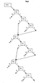
- FIG. 5 shows, for example, the binary decision diagram T v (s 1 ) obtained by successively replacing each of the binary decision diagrams in the formulas given above for T v (s 1 ) by the binary decision diagrams T v ( s i ), T c (s i ), for s equal to s 5 , s 6 , s 7 , s 8 , s 9 , s 10 .
- each of the binary decision diagrams T c (s 5 ), T c (s 6 ), T c (s 7 ), T c (s 8 ), T c (s 9 ), T c (s 10 ) is equal to 1 and where each of the binary decision diagrams T v (s 5 ) , T v (s 6 ), T v (s 7 ), T v (s 8 ), T v (s 9 ), T v (s 10 ), is replaced respectively by each of the binary decision diagrams ⁇ x v5 ; 0; 1 ⁇ , ⁇ xv6 ; 0; 1 ⁇ , ⁇ xv7 ; 0; 1 ⁇ , ⁇ xv8 ; 0; 1 ⁇ , ⁇ xv9 ; 0; 1 ⁇ , ⁇ xv10 ; 0;
- the binary decision diagram T 1 (s 1 ) is traversed on each leading branch of the node occupied by the variable x v5 , to a sheet occupied by the value 1, keeping in a logical conjunction each variable x v5 , x v6 , x v7 , x v8 , x v9 , x v10 encountered as it is if the path of the branch is continued by means of the right pointer and complemented if the course of the branch is continued by means of the left pointer.
- Each logical conjunction obtained by the path on a branch is kept in a logical disjunction until it has traveled all the branches leading to a sheet occupied by the value 1. This gives the logic equation of the circuit of FIG.
- s 1 + s 5 ⁇ s 6 ⁇ s 7 ⁇ s 8 ⁇ s 9 ⁇ s 10+ s 5 ⁇ s 6 ⁇ s 7 ⁇ s 8 ⁇ s 9+ s 5 ⁇ s 6 ⁇ s 7 ⁇ s 9 ⁇ s 10 + s 5 ⁇ s 7 ⁇ s 8 ⁇ s 9+ s 5 ⁇ s 7 ⁇ s 8 ⁇ s 9 ⁇ s 10+ s 5 ⁇ s 7 ⁇ s 9 ⁇ s 10+ s 5 ⁇ s 7 ⁇ s 9 ⁇ s 10+ s 5. s 6. s 7. s 9
- the elementary circuit element of FIG. 4 comprises two NMOS transistors 34 and 35 whose sources are respectively etched by the signals s 16 and s 18 , whose gates are respectively etched by the signals s 17 and s 19 , and whose the drains respectively generate signals s 13 and s 14 on conductors 29 and 30.
- the elementary circuit element of FIG. 4 also comprises two PMOS transistors 37 and 36, the sources of which are respectively etched by the signal s 21 and a signal s 20 , whose grids are respectively attacked by the signals s 17 and s 19 , and whose drains respectively generate the signal s 20 and a signal s 15 on conductors 32 and 31.
- the conductors 29, 30 and 31 are connected to a driver 28 at a point 33.
- the fifth step scans ( scan in English) each of the signals s 16 , s 17 , s 18 , s 19 , s 21 , of the connector list and for each signal scanned, performs the first two steps.
- the binary decision diagrams T v (s 16 ), T c (s 16 ), T e (s 16 ), T v (s 18 ), T c (s 18 ), T e (s 18 ) are respectively equal to singletons ⁇ 0 ⁇ , ⁇ 1 ⁇ , ⁇ 0 ⁇ , ⁇ 0 ⁇ , ⁇ 1 ⁇ , ⁇ 0 ⁇ .
- the binary decision diagrams T v (s 21 ), T c (s 21 ), T e (s 21 ) are respectively equal to the singletons ⁇ 1 ⁇ , ⁇ 1 ⁇ , ⁇ 0 ⁇ .
- the binary decision diagrams T v (s 17 ), T c (s 17 ), T e (s 17 ), are respectively ⁇ x v17 , 0,1 ⁇ , ⁇ 1 ⁇ , ⁇ 0 ⁇ .
- the binary decision diagrams T v (s 19 ), T c (s 19 ), T e (s 19 ) are respectively ⁇ x v19 , 0,1 ⁇ , ⁇ 1 ⁇ , ⁇ 0 ⁇ .
- the sixth step then scans the elements of the elementary circuit attacked by the signals s 16 , s 17 , s 18 , s 19 , s 21 , of the list of connectors and associates with the transistors 34, 35, 37, respectively, the signals s 13 , s 14 , s 20 , for each of which she performs the first two steps.
- the sixth step is restarted to scan the elements of the elementary circuit attacked by the previously generated signals s 13 , s 14 , s 20 , of the connector list and associates with these elements which are the point 33 and the transistor 36, respectively the signals s 22 , s 15 , for each of which she performs the first two steps.
- the sixth step is restarted to scan the elements of the elementary circuit attacked by the previously generated signals s 22 , s 15 , of the connector list and associates with the only found element which is the point 33, the signal s 12 for which it executes the first two steps.
- the circuit of FIG. 4 is recognized as a gate NOR.
- a first decision diagram binary leads to 1 when the signal state with which it is associated is a high state impedance Z or a logic state H
- a second binary decision diagram leads to 1 when the signal state with which it is associated is a logic state B or a logic state H
- a third binary decision diagram leads to 1 when the state of the signal to which it is associated is an error state E.
- the skilled person can easily take advantage of the teaching of the invention by otherwise defining the three binary decision diagrams, for example the first one binary decision diagram leads to 1 when the signal state with which it is associated is a state of high impedance Z or a logic state H, the second decision diagram binary leads to 1 when the signal state with which it is associated is a high state impedance Z or a logic state B, the third binary decision diagram leads to 1 when the signal state with which it is associated is an error state E.
- the skilled person can define other binary decision diagrams to each code positively a presence of one or two of several possible states, negatively an absence of this or these two possible states.
- the first binary decision diagram T v (s i ) leads to 0 if the state of the signal is not the state H
- the first binary decision diagram T v (s i ) then leads to 0 if the state of the signal is the state B.
- the binary decision diagram T c (s i ) leads to 1, driving to 1 for the binary decision diagram T v (s i ), referred to as value, indicates a logic state H of the signal s i , leading to 0, indicates a logic state B of the signal s i .
Landscapes
- Engineering & Computer Science (AREA)
- General Engineering & Computer Science (AREA)
- Physics & Mathematics (AREA)
- General Physics & Mathematics (AREA)
- Tests Of Electronic Circuits (AREA)
- Design And Manufacture Of Integrated Circuits (AREA)
- Investigating Or Analysing Biological Materials (AREA)
- Logic Circuits (AREA)
- Automatic Analysis And Handling Materials Therefor (AREA)
- Transition And Organic Metals Composition Catalysts For Addition Polymerization (AREA)
- Semiconductor Integrated Circuits (AREA)
Claims (12)
- Verfahren zum Codieren von mehr als zwei möglichen Zuständen (H, B, Z) eines ersten Signals (si), dadurch gekennzeichnet, dass es umfasst:einen ersten Schritt, der dem ersten Signal (si) eine erste binäre Variable (xci), wovon ein erster Wert (1) angibt, dass das erste Signal (si) in einem ersten Zustand (H) oder in einem zweiten Zustand (B) ist, eine zweite binäre Variable (xvi), wovon ein erster Wert (1) angibt, dass das erste Signal (si) in dem ersten Zustand (H) oder in einem dritten Zustand (Z) ist, ein erstes binäres Entscheidungsdiagramm (Tc(si)) und ein zweites binäres Entscheidungsdiagramm (Tv(si)) zuordnet; undeinen zweiten Schritt, der das erste binäre Entscheidungsdiagramm (Tc(si)) mittels einer ersten Regel (Rc) konstruiert, die das erste binäre Entscheidungsdiagramm (Tc(si)) zu einem ersten Wert (1) führt, wenn die erste binäre Variable (xci) ihren ersten Wert (1) hat, und der das zweite binäre Entscheidungsdiagramm (Tv(si)) mittels einer zweiten Regel (Rv) konstruiert, die das zweite binäre Entscheidungsdiagramm (Tv(si)) zu dem ersten Wert (1) führt, wenn die zweite binäre Variable (xvi) ihren ersten Wert (1) hat.
- Verfahren nach Anspruch 1, dadurch gekennzeichnet, dass dann, wenn das erste Signal (si) durch eine elementare Entität erzeugt wird, die am Eingang eines oder mehrere zweite Signale (si+1, si+2) empfängt, auf die der erste und der zweite Schritt angewendet werden, dieser Entität eine erste kombinatorische Operation (Φc) und eine zweite kombinatorische Operation (Φv) zugeordnet werden, wobei die erste kombinatorische Operation (Φc) den Wert der ersten binären Variable (xci), die dem ersten Signal (si) zugeordnet ist, in Abhängigkeit vom Wert jeder der ersten binären Variablen (xci+1, xci+2), die dem bzw. den zweiten Signalen (si+1, si+2) zugeordnet sind, und in Abhängigkeit vom Wert jeder der zweiten binären Variablen (xvi+1, xvi+2), die dem bzw. den zweiten Signalen (si+1, si+2) zugeordnet sind, ergibt und wobei die zweite kombinatorische Operation (Φv) den Wert der zweiten binären Variable (xvi), die dem ersten Signal (si) zugeordnet ist, in Abhängigkeit vom Wert jeder der ersten binären Variablen (xci+1, xci+2), die dem bzw. den zweiten Signalen (si+1, si+2) zugeordnet sind, und in Abhängigkeit vom Wert jeder der zweiten binären Variablen (xvi+1, xvi+2), die dem bzw. den zweiten Signalen (si+1, si+2) zugeordnet sind, ergibt.
- Verfahren nach Anspruch 2, dadurch gekennzeichnet, dass die erste Regel (Rc) das erste binäre Entscheidungsdiagramm (Tc(si)), das dem ersten Signal (si) zugeordnet ist, dadurch konstruiert, dass sie in der ersten kombinatorischen Operation (Φc) jede der ersten binären Variablen (xci+1, xci+2), die den zweiten Signalen (si+1, si+2) zugeordnet sind, durch jedes der ersten binären Entscheidungsdiagramme (Tc(si+1), Tc(si+2)), die den zweiten Signalen (si+1, si+2) zugeordnet sind, ersetzt und jede der zweiten binären Variablen (xvi+1, xvi+2), die den zweiten Signalen (si+1, si+2) zugeordnet sind, durch jedes der zweiten binären Entscheidungsdiagramme (Tv(si+1), Tv(si+2)), die den zweiten Signalen (si+1, si+2) zugeordnet sind, ersetzt.
- Verfahren nach Anspruch 2 oder 3, dadurch gekennzeichnet, dass die zweite Regel (Rv) das zweite binäre Entscheidungsdiagramm (Tv(si)), das dem ersten Signal (si) zugeordnet ist, dadurch konstruiert, dass es in der zweiten kombinatorischen Operation (Φv) jede der ersten binären Variablen (xci+1, xci+2), die den zweiten Signalen (si+1, si+2) zugeordnet sind, durch jedes der ersten binären Entscheidungsdiagramme (Tc(si+1), Tc(si+2)), die den zweiten Signalen (si+1, si+2) zugeordnet sind, ersetzt und jede der zweiten binären Variablen (xvi+1, xvi+2), die den zweiten Signalen (si+1, si+2) zugeordnet sind, durch jedes der zweiten binären Entscheidungsdiagramme (Tv(si+1), Tv(si+2)), die den zweiten Signalen (si+1, si+2) zugeordnet sind, ersetzt.
- Verfahren nach Anspruch 1, dadurch gekennzeichnet, dass die erste Regel (Rc) dann, wenn das erste Signal (si) von keinem anderen Signal (si) abhängt, das erste binäre Entscheidungsdiagramm (Tc(si)), das dem ersten Signal (si) zugeordnet ist, dadurch konstruiert, dass sie ein Triplett ({No, Pg, Pd}) erzeugt, das einen von der ersten Variable (xci) besetzten Knoten (No), einen linken Zeiger (Pg) auf den zweiten Wert (0) und einen rechten Zeiger (Pd) auf den zweiten Wert (1) umfasst.
- Verfahren nach Anspruch 1 oder 5, dadurch gekennzeichnet, dass die zweite Regel (Rv) dann, wenn das erste Signal (si) von keinem anderen Signal (si) abhängt, das zweite binäre Entscheidungsdiagramm (Tv(si)), das dem ersten Signal (si) zugeordnet ist, dadurch konstruiert, dass es ein Triplett ({No', Pg', Pd'}) erzeugt, das einen von der ersten Variable (xvi) besetzten Knoten (No'), einen linken Zeiger (Pg') auf den zweiten Wert (0) und einen rechten Zeiger (Pd') auf den zweiten Wert (1) umfasst.
- Verfahren nach einem der Ansprüche 1 bis 6, dadurch gekennzeichnet, dass:der erste Schritt dem ersten Signal (si) ein drittes binäres Entscheidungsdiagramm (Te(si)) zuordnet; undder zweite Schritt das dritte binäre Entscheidungsdiagramm (Te(si)) mittels einer dritten Regel (Re) konstruiert, die das dritte binäre Entscheidungsdiagramm (Te(si)) zu dem ersten Wert (1) führt, wenn die erste binäre Variable (xci) nicht ihren ersten Wert (1) hat und wenn die zweite binäre Variable (xvi) nicht ihren ersten Wert (1) hat.
- Verfahren nach Anspruch 7, dadurch gekennzeichnet, dass dann, wenn das erste Signal (si) durch eine elementare Entität erzeugt wird, die am Eingang eines oder mehrere zweite Signale (si+1, si+2) empfängt, auf die der erste und der zweite Schritt angewendet werden, dieser Entität eine dritte kombinatorische Operation (Φe) zugeordnet wird, wobei die dritte kombinatorische Operation (Φe) einen zweiten Wert der ersten binären Variable (xci) und einen zweiten Wert der zweiten binären Variable (xvi), die dem ersten Signal (si) zugeordnet sind, in Abhängigkeit vom Wert jeder der ersten binären Variablen (xci+1, xci+2), die dem bzw. den zweiten Signalen (si+1, si+2) zugeordnet sind, und in Abhängigkeit vom Wert jeder der zweiten binären Variablen (xvi+1, xvi+2), die dem bzw. den zweiten Signalen (si+1, si+2) zugeordnet sind, ergibt.
- Verfahren nach Anspruch 8, dadurch gekennzeichnet, dass die dritte Regel (Re) das dritte binäre Entscheidungsdiagramm (Te(si)), das dem ersten Signal (si) zugeordnet ist, dadurch konstruiert, dass sie in der dritten kombinatorischen Operation (Φe) jede der ersten binären Variablen (xci+1, xci+2), die den zweiten Signalen (si+1, si+2) zugeordnet sind, durch jedes der ersten binären Entscheidungsdiagramme (Tc(si+1), Tc(si+2)), die den zweiten Signalen (si+1, si+2) zugeordnet sind, ersetzt und jede der zweiten binären Variablen (xvi+1, xvi+2), die den zweiten Signalen (si+1, si+2) zugeordnet sind, durch jedes der zweiten binären Entscheidungsdiagramme (Tv(si+1), Tv(si+2)), die den zweiten Signalen (si+1, si+2) zugeordnet sind, ersetzt.
- Datenverarbeitungssystem, das wenigstens einen Prozessor und einen Speicher enthält, dadurch gekennzeichnet, dass der Speicher ein Programm für die Ausführung des Verfahrens nach einem der Ansprüche 1 bis 9 enthält.
- Rechnerprogramm, das Programmcode-Teile/-Mittel/-Befehle, die das Verfahren nach einem der Ansprüche 1 bis 9 ausführen, wenn das Programm auf einem Datenverarbeitungssystem ausgeführt wird, umfasst.
- Aufzeichnungsträger für Rechnerprogramm, dadurch gekennzeichnet, dass er ein Programm enthält, das von einer Maschine eines Datenverarbeitungssystems lesbar ist, um die Ausführung des Verfahrens nach einem der Ansprüche 1 bis 9 zu steuern.
Applications Claiming Priority (3)
| Application Number | Priority Date | Filing Date | Title |
|---|---|---|---|
| FR0007354 | 2000-06-08 | ||
| FR0007354A FR2810126B1 (fr) | 2000-06-08 | 2000-06-08 | Outil automatique d'analyse de testabilite |
| PCT/FR2001/001764 WO2001094960A1 (fr) | 2000-06-08 | 2001-06-07 | Outil automatique d'analyse de testabilite |
Publications (2)
| Publication Number | Publication Date |
|---|---|
| EP1292839A1 EP1292839A1 (de) | 2003-03-19 |
| EP1292839B1 true EP1292839B1 (de) | 2004-05-06 |
Family
ID=8851099
Family Applications (1)
| Application Number | Title | Priority Date | Filing Date |
|---|---|---|---|
| EP01943583A Expired - Lifetime EP1292839B1 (de) | 2000-06-08 | 2001-06-07 | Automatisches gerät für testbarkeitsanalyse |
Country Status (6)
| Country | Link |
|---|---|
| US (1) | US20020156540A1 (de) |
| EP (1) | EP1292839B1 (de) |
| AT (1) | ATE266209T1 (de) |
| DE (1) | DE60103154T2 (de) |
| FR (1) | FR2810126B1 (de) |
| WO (1) | WO2001094960A1 (de) |
Families Citing this family (3)
| Publication number | Priority date | Publication date | Assignee | Title |
|---|---|---|---|---|
| US7551572B2 (en) * | 2005-10-21 | 2009-06-23 | Isilon Systems, Inc. | Systems and methods for providing variable protection |
| US7739635B2 (en) * | 2007-05-10 | 2010-06-15 | International Business Machines Corporation | Conjunctive BDD building and variable quantification using case-splitting |
| CN104515950B (zh) * | 2015-01-12 | 2018-05-22 | 华南师范大学 | 一种集成电路的内建自测试方法及应用 |
Family Cites Families (4)
| Publication number | Priority date | Publication date | Assignee | Title |
|---|---|---|---|---|
| US5481717A (en) * | 1993-04-12 | 1996-01-02 | Kabushiki Kaisha Toshiba | Logic program comparison method for verifying a computer program in relation to a system specification |
| US5572535A (en) * | 1994-07-05 | 1996-11-05 | Motorola Inc. | Method and data processing system for verifying the correct operation of a tri-state multiplexer in a circuit design |
| US5752000A (en) * | 1994-08-02 | 1998-05-12 | Cadence Design Systems, Inc. | System and method for simulating discrete functions using ordered decision arrays |
| FR2810127B1 (fr) * | 2000-06-08 | 2002-08-16 | Bull Sa | Procede pour mettre en evidence la dependance d'un signal en fonction d'un autre signal |
-
2000
- 2000-06-08 FR FR0007354A patent/FR2810126B1/fr not_active Expired - Fee Related
-
2001
- 2001-06-07 DE DE60103154T patent/DE60103154T2/de not_active Expired - Lifetime
- 2001-06-07 EP EP01943583A patent/EP1292839B1/de not_active Expired - Lifetime
- 2001-06-07 US US10/049,023 patent/US20020156540A1/en not_active Abandoned
- 2001-06-07 AT AT01943583T patent/ATE266209T1/de not_active IP Right Cessation
- 2001-06-07 WO PCT/FR2001/001764 patent/WO2001094960A1/fr not_active Ceased
Also Published As
| Publication number | Publication date |
|---|---|
| DE60103154T2 (de) | 2005-06-09 |
| FR2810126A1 (fr) | 2001-12-14 |
| EP1292839A1 (de) | 2003-03-19 |
| DE60103154D1 (de) | 2004-06-09 |
| ATE266209T1 (de) | 2004-05-15 |
| US20020156540A1 (en) | 2002-10-24 |
| FR2810126B1 (fr) | 2004-03-12 |
| WO2001094960A1 (fr) | 2001-12-13 |
Similar Documents
| Publication | Publication Date | Title |
|---|---|---|
| Thakur et al. | Current issues and emerging techniques for VLSI testing-A review☆ | |
| US20190220776A1 (en) | Multi-Stage Machine Learning-Based Chain Diagnosis | |
| EP3443369B1 (de) | System und verfahren zum testen einer integrierten schaltung | |
| Leininger et al. | Compression mode diagnosis enables high volume monitoring diagnosis flow | |
| FR3066606B1 (fr) | Appareil de test et procede de test d'un circuit integre | |
| US6732312B2 (en) | Test vector compression method | |
| WO2001094960A1 (fr) | Outil automatique d'analyse de testabilite | |
| JPH0894720A (ja) | 論理回路における試験不能欠陥を特定する方法 | |
| Chung et al. | Majority logic circuits optimisation by node merging | |
| EP1716425B1 (de) | Verfahren zum erzeugen von hdl-beschreibungsdateien digitaler systeme und erhaltene systeme | |
| EP1292840B1 (de) | Verfahren zum nachweisen der abhängigkeit eines signals von einem anderen signal | |
| EP0762285A1 (de) | Prüfbares elektronisches System | |
| EP0541170B1 (de) | Verfahren und Einrichtung zum Aufspüren einer vorspezifizierten Teilschaltung in einer elektrischen Schaltung, Verfahren zum Erstellen von Masken für Integrierte Schaltungen unter Benutzung des Verfahrens | |
| US6804803B2 (en) | Method for testing integrated logic circuits | |
| US20240160823A1 (en) | Test Generation for Structurally Similar Circuits | |
| FR3131413A1 (fr) | Réseau de neurones avec génération à la volée des paramètres du réseau | |
| Pomeranz et al. | Diagnostic test generation based on subsets of faults | |
| US20020112215A1 (en) | Method and system for finding static NAND and NOR gates within a circuit and identifying the constituent FETs each gate | |
| FR3010207A1 (fr) | Procede d'analyse du comportement d'un circuit integre mis en œuvre par ordinateur et comprenant la selection de chemins sur la base de plusieurs criteres appartenant a des types differents | |
| Sanjay et al. | Verilog based Architecture Computing Testability Measures for DFT Designers | |
| FR3010811A1 (fr) | Procede de determination du dimensionnement des transistors d'un circuit analogique | |
| US20060190898A1 (en) | Net list producing device producing a net list with an interconnection parasitic element by hierarchical processing | |
| FR2814825A1 (fr) | Procede pour convertir des expressions conditionnelles depuis un langage de description materiel non verilog en un langage de description materiel verilog tout en sauvegardant une structure appropriee pour la synthese logique | |
| WO2025183730A1 (en) | Fault partition node systems for circuit design, test and diagnosis | |
| FLORIA | A STRUCTURAL FAULT COLLAPSING ALGORITHM AND THE APPLICATION OF MACHINE LEARNING TO APPROXIMATE THE NUMBER OF COLLAPSED FAULTS |
Legal Events
| Date | Code | Title | Description |
|---|---|---|---|
| PUAI | Public reference made under article 153(3) epc to a published international application that has entered the european phase |
Free format text: ORIGINAL CODE: 0009012 |
|
| 17P | Request for examination filed |
Effective date: 20030108 |
|
| AK | Designated contracting states |
Kind code of ref document: A1 Designated state(s): AT BE CH CY DE DK ES FI FR GB GR IE IT LI LU MC NL PT SE TR |
|
| GRAP | Despatch of communication of intention to grant a patent |
Free format text: ORIGINAL CODE: EPIDOSNIGR1 |
|
| GRAS | Grant fee paid |
Free format text: ORIGINAL CODE: EPIDOSNIGR3 |
|
| GRAA | (expected) grant |
Free format text: ORIGINAL CODE: 0009210 |
|
| AK | Designated contracting states |
Kind code of ref document: B1 Designated state(s): AT BE CH CY DE DK ES FI FR GB GR IE IT LI LU MC NL PT SE TR |
|
| PG25 | Lapsed in a contracting state [announced via postgrant information from national office to epo] |
Ref country code: CY Free format text: LAPSE BECAUSE OF FAILURE TO SUBMIT A TRANSLATION OF THE DESCRIPTION OR TO PAY THE FEE WITHIN THE PRESCRIBED TIME-LIMIT Effective date: 20040506 Ref country code: AT Free format text: LAPSE BECAUSE OF FAILURE TO SUBMIT A TRANSLATION OF THE DESCRIPTION OR TO PAY THE FEE WITHIN THE PRESCRIBED TIME-LIMIT Effective date: 20040506 Ref country code: TR Free format text: LAPSE BECAUSE OF FAILURE TO SUBMIT A TRANSLATION OF THE DESCRIPTION OR TO PAY THE FEE WITHIN THE PRESCRIBED TIME-LIMIT Effective date: 20040506 Ref country code: FI Free format text: LAPSE BECAUSE OF FAILURE TO SUBMIT A TRANSLATION OF THE DESCRIPTION OR TO PAY THE FEE WITHIN THE PRESCRIBED TIME-LIMIT Effective date: 20040506 Ref country code: NL Free format text: LAPSE BECAUSE OF FAILURE TO SUBMIT A TRANSLATION OF THE DESCRIPTION OR TO PAY THE FEE WITHIN THE PRESCRIBED TIME-LIMIT Effective date: 20040506 Ref country code: IE Free format text: LAPSE BECAUSE OF FAILURE TO SUBMIT A TRANSLATION OF THE DESCRIPTION OR TO PAY THE FEE WITHIN THE PRESCRIBED TIME-LIMIT Effective date: 20040506 |
|
| REG | Reference to a national code |
Ref country code: GB Ref legal event code: FG4D Free format text: NOT ENGLISH |
|
| REG | Reference to a national code |
Ref country code: CH Ref legal event code: EP |
|
| GBT | Gb: translation of ep patent filed (gb section 77(6)(a)/1977) |
Effective date: 20040506 |
|
| PG25 | Lapsed in a contracting state [announced via postgrant information from national office to epo] |
Ref country code: LU Free format text: LAPSE BECAUSE OF NON-PAYMENT OF DUE FEES Effective date: 20040607 |
|
| REF | Corresponds to: |
Ref document number: 60103154 Country of ref document: DE Date of ref document: 20040609 Kind code of ref document: P |
|
| REG | Reference to a national code |
Ref country code: IE Ref legal event code: FG4D Free format text: FRENCH |
|
| PG25 | Lapsed in a contracting state [announced via postgrant information from national office to epo] |
Ref country code: BE Free format text: LAPSE BECAUSE OF NON-PAYMENT OF DUE FEES Effective date: 20040630 Ref country code: MC Free format text: LAPSE BECAUSE OF NON-PAYMENT OF DUE FEES Effective date: 20040630 |
|
| PG25 | Lapsed in a contracting state [announced via postgrant information from national office to epo] |
Ref country code: GR Free format text: LAPSE BECAUSE OF FAILURE TO SUBMIT A TRANSLATION OF THE DESCRIPTION OR TO PAY THE FEE WITHIN THE PRESCRIBED TIME-LIMIT Effective date: 20040806 Ref country code: SE Free format text: LAPSE BECAUSE OF FAILURE TO SUBMIT A TRANSLATION OF THE DESCRIPTION OR TO PAY THE FEE WITHIN THE PRESCRIBED TIME-LIMIT Effective date: 20040806 Ref country code: DK Free format text: LAPSE BECAUSE OF FAILURE TO SUBMIT A TRANSLATION OF THE DESCRIPTION OR TO PAY THE FEE WITHIN THE PRESCRIBED TIME-LIMIT Effective date: 20040806 |
|
| PG25 | Lapsed in a contracting state [announced via postgrant information from national office to epo] |
Ref country code: ES Free format text: LAPSE BECAUSE OF FAILURE TO SUBMIT A TRANSLATION OF THE DESCRIPTION OR TO PAY THE FEE WITHIN THE PRESCRIBED TIME-LIMIT Effective date: 20040817 |
|
| NLV1 | Nl: lapsed or annulled due to failure to fulfill the requirements of art. 29p and 29m of the patents act | ||
| REG | Reference to a national code |
Ref country code: IE Ref legal event code: FD4D |
|
| BERE | Be: lapsed |
Owner name: BULL S.A. Effective date: 20040630 |
|
| PLBE | No opposition filed within time limit |
Free format text: ORIGINAL CODE: 0009261 |
|
| STAA | Information on the status of an ep patent application or granted ep patent |
Free format text: STATUS: NO OPPOSITION FILED WITHIN TIME LIMIT |
|
| 26N | No opposition filed |
Effective date: 20050208 |
|
| PG25 | Lapsed in a contracting state [announced via postgrant information from national office to epo] |
Ref country code: CH Free format text: LAPSE BECAUSE OF NON-PAYMENT OF DUE FEES Effective date: 20050630 Ref country code: LI Free format text: LAPSE BECAUSE OF NON-PAYMENT OF DUE FEES Effective date: 20050630 |
|
| REG | Reference to a national code |
Ref country code: CH Ref legal event code: PL |
|
| PG25 | Lapsed in a contracting state [announced via postgrant information from national office to epo] |
Ref country code: PT Free format text: LAPSE BECAUSE OF NON-PAYMENT OF DUE FEES Effective date: 20041006 |
|
| REG | Reference to a national code |
Ref country code: FR Ref legal event code: PLFP Year of fee payment: 16 |
|
| REG | Reference to a national code |
Ref country code: FR Ref legal event code: PLFP Year of fee payment: 17 |
|
| REG | Reference to a national code |
Ref country code: FR Ref legal event code: PLFP Year of fee payment: 18 |
|
| PGFP | Annual fee paid to national office [announced via postgrant information from national office to epo] |
Ref country code: FR Payment date: 20200626 Year of fee payment: 20 |
|
| PGFP | Annual fee paid to national office [announced via postgrant information from national office to epo] |
Ref country code: GB Payment date: 20200629 Year of fee payment: 20 Ref country code: IT Payment date: 20200618 Year of fee payment: 20 |
|
| PGFP | Annual fee paid to national office [announced via postgrant information from national office to epo] |
Ref country code: DE Payment date: 20200827 Year of fee payment: 20 |
|
| REG | Reference to a national code |
Ref country code: DE Ref legal event code: R071 Ref document number: 60103154 Country of ref document: DE |
|
| REG | Reference to a national code |
Ref country code: GB Ref legal event code: PE20 Expiry date: 20210606 |
|
| PG25 | Lapsed in a contracting state [announced via postgrant information from national office to epo] |
Ref country code: GB Free format text: LAPSE BECAUSE OF EXPIRATION OF PROTECTION Effective date: 20210606 |