EP1290799B1 - Phasenverriegelungsschaltung - Google Patents
Phasenverriegelungsschaltung Download PDFInfo
- Publication number
- EP1290799B1 EP1290799B1 EP01938837A EP01938837A EP1290799B1 EP 1290799 B1 EP1290799 B1 EP 1290799B1 EP 01938837 A EP01938837 A EP 01938837A EP 01938837 A EP01938837 A EP 01938837A EP 1290799 B1 EP1290799 B1 EP 1290799B1
- Authority
- EP
- European Patent Office
- Prior art keywords
- charge pump
- circuit
- pump circuit
- output
- signal
- Prior art date
- Legal status (The legal status is an assumption and is not a legal conclusion. Google has not performed a legal analysis and makes no representation as to the accuracy of the status listed.)
- Expired - Lifetime
Links
Images


Classifications
-
- H—ELECTRICITY
- H03—ELECTRONIC CIRCUITRY
- H03L—AUTOMATIC CONTROL, STARTING, SYNCHRONISATION OR STABILISATION OF GENERATORS OF ELECTRONIC OSCILLATIONS OR PULSES
- H03L7/00—Automatic control of frequency or phase; Synchronisation
- H03L7/06—Automatic control of frequency or phase; Synchronisation using a reference signal applied to a frequency- or phase-locked loop
- H03L7/08—Details of the phase-locked loop
- H03L7/085—Details of the phase-locked loop concerning mainly the frequency- or phase-detection arrangement including the filtering or amplification of its output signal
- H03L7/089—Details of the phase-locked loop concerning mainly the frequency- or phase-detection arrangement including the filtering or amplification of its output signal the phase or frequency detector generating up-down pulses
- H03L7/0891—Details of the phase-locked loop concerning mainly the frequency- or phase-detection arrangement including the filtering or amplification of its output signal the phase or frequency detector generating up-down pulses the up-down pulses controlling source and sink current generators, e.g. a charge pump
-
- H—ELECTRICITY
- H03—ELECTRONIC CIRCUITRY
- H03L—AUTOMATIC CONTROL, STARTING, SYNCHRONISATION OR STABILISATION OF GENERATORS OF ELECTRONIC OSCILLATIONS OR PULSES
- H03L7/00—Automatic control of frequency or phase; Synchronisation
- H03L7/06—Automatic control of frequency or phase; Synchronisation using a reference signal applied to a frequency- or phase-locked loop
- H03L7/16—Indirect frequency synthesis, i.e. generating a desired one of a number of predetermined frequencies using a frequency- or phase-locked loop
- H03L7/18—Indirect frequency synthesis, i.e. generating a desired one of a number of predetermined frequencies using a frequency- or phase-locked loop using a frequency divider or counter in the loop
Definitions
- This invention relates to a phase lock circuit
- a phase frequency comparator having a first input for a reference signal and a second input for a feedback signal, as well as outputs for furnishing an up-signal or a down-signal to a control charge pump circuit
- control charge pump circuit is connected with the outputs of the phase frequency comparator and has an output which is connected via a loop filter with a voltage-controlled oscillator provided with tuning means, the output of the oscillator being connected via a frequency divider with said second input of the phase frequency comparator, wherein for furnishing a tuning voltage for the tuning means a voltage charge pump circuit is provided, which is combined with the control charge pump circuit to form a combined charge pump circuit connected with the output of the phase frequency comparator.
- a high-quality voltage-controlled oscillator with a low phase noise is tuned with the aid of a varactor.
- a problem occurring in the known phase lock circuits and in particular with integrated phase lock circuits is that in many applications the supply voltage is too low to realize the tuning voltage range needed for the varactor. In applications for, for instance, pagers, cordless phones, cellular phones, etc., often a 1.5 V battery in used, while for a varactor a tuning voltage range of, for instance, 0.6-8 V may be required.
- step-up converter which can generate a supply voltage which is higher than the battery voltage.
- a drawback of this solution is that it requires a coil of high self-induction, which cannot be formed on a chip. This results in an increase of the number of required components and the manufacturing costs of the circuit, as well as of the space occupied and the chance of parasitic effects as a result of the necessary connections between the circuit section on the chip and the off-chip coil.
- a charge pump circuit could be used to generate a voltage higher than the battery voltage.
- An example of such a charge pump is described in IEEE JSSC Vol. 33 No. 4, April 1998.
- a phase locked loop circuit with a charge pump is known form the European patent application 0 945 986.
- a problem inherent to that solution is that such a charge pump circuit must have a lower output impedance than the, already low, output impedance of the low-pass filter, which loads the output of the phase frequency comparator.
- phase locked loop circuit is known too.
- This '747 publication describes a phase locked loop with a phase comparator in which the outputs of the phase comparator are connected to a voltage multiplier circuit which controls the voltage controlled oscillator of the phase locked loop.
- the voltage multiplier circuit is both a control charge pump for the oscillator and a voltage charge pump which increases the voltage range.
- One output of the phase/frequency comparator of the phase locked loop is connected to the gate of a first transistor, while smother output of the comparator is connected to ground via a capacitor and a first diode.
- a second transistor is connected with the gate to ground and with the drain to capacitor-first diode node.
- the first transistor and the second transistor are connected to each other via a second diode.
- An RC-filter is connected to the node between first transistor and second diode.
- the United States patent publication 5 623 523 describes a PLL in which two seperate charge pumps are combined, one for the PLL loopfilter and one for the power supply voltage.
- the charge pump for the power supply voltage only generates the higher power supply voltage for the PLL-charge pump and the PLL-charge pump uses this higher power supply voltage for the PLL charge-pump. Thereby, the same clock signal is used for both charge pumps.
- the international patent publication WO 99 21282 describes a similar circuit.
- the European patent publication 283 160 describes a phase comparator of which the output signal may have four or more values. A current source is connected to each of the outputs of the comparator. The current source may be switched on and off by the output signal.
- a phase lock circuit of the above type is characterized in that the combined charge pump circuit comprises two transistor each operatively controlled by a clock signal in combination with the up-signal, which transistor elements are alternately connected with successive capacitors of the combined charge pump circuit, and a third transistor element is provided which is connected between the output of the combined charge pump circuit and earth and which is operatively controlled by the down-signal.
- Fig. 1 schematically shows an example of a known phase lock circuit 1.
- the phase lock circuit 1 shown comprises a phase frequency comparator 2 with two inputs 3, 4 and two outputs 6, 6.
- the input 3 in operation receives a reference signal and the input 4 is connected with the output 7 of a feedback circuit 8, which comprises a frequency divider.
- the phase lock circuit is provided in a conventional manner with supply voltage Vcc, supplied by a battery (not shown), via supply terminals "+" and "-".
- the phase frequency comparator compares the frequency of the two input signals and, depending on the result of that comparison, produces an up- or down-signal.
- the output signals of the phase frequency comparator are fed to the gates G1 and G2, respectively, of two MOS transistors M1 and M2, which are connected between the positive and the negative supply connections, and which jointly form a charge pump 9, which produces a control signal on an output 10.
- the output 10 is connected with a low-pass filter or loop filter 11 which, in the example shown, comprises a capacitor C1 parallel to a series connection of a capacitor C2 and a resistor R1.
- An up-signal brings the transistor M1 into the conducting state, so that the RC network connected with output 10 of the charge pump is charged with a constant current
- a down-signal brings transistor M2 into the conducting state, so that the RC network connected with the output 10 is discharged with a constant current
- the output 10 is further connected via the loop filter 11 with a varactor 12, which constitutes a part of a voltage-controlled oscillator (VCO) 13, and so do a coil L and a capacitor C3.
- VCO voltage-controlled oscillator
- the output 10 of the charge pump 9 cannot furnish a higher voltage than the supply voltage Vcc.
- the control voltage for the varactor, and hence the tuning voltage range for the VCO 13, is therefore limited by the battery voltage.
- step-up converter (not shown) is used as a voltage boost circuit between the battery and the supply voltage terminals of the charge pump.
- the output 15 of the VCO furnishes the desired phase-locked output signal and is further connected with the input 16 of the frequency divider 8 already mentioned.
- a drawback of a step-up converter is that the coil of high self-induction of the voltage boost circuit cannot be integrated on a chip and moreover is relatively sizable.
- the coil therefore constitutes an off-chip component, for which separate connections are needed, and which takes up extra space.
- Fig. 2 schematically shows an example of a different type of voltage boost circuit 20, which is designed as a voltage charge pump, known per se.
- the aim of the invention is the use of such a voltage charge pump in a phase lock circuit.
- the voltage charge pump shown can be produced wholly in integrated form and can moreover furnish an output voltage which is higher than the voltage of the supply battery B.
- the voltage charge pump actually comprises a capacitor network switched by means of semiconductor switching elements, for instance MOS transistors T21 to T25, which network, in the example shown, comprises capacitors C21 to C25. Switching is done with the aid of clock signals furnished by clock circuits 21a and 21b which are respectively connected with the capacitors C21, C23 and C22, C24, respectively. Capacitor C25 is connected between the output 22 of the voltage charge pump and earth.
- the clock signals are usually the same signals, which, however, are in antiphase.
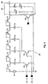
- Fig. 3 schematically shows an example of a voltage charge pump 20 of the type shown in Fig. 2, combined with the control charge pump 9 of the circuit of Fig. 1.
- the transistors (or arrays of transistors) M3 and M4 are controlled by the clock signals CL and CL together with the up-signal of output 5 of Fig. 1, with the understanding that the clock signals (and hence the voltage boost effect) only occur if an up-signal is present.
- the transistors M3 and M4 are comparable to transistor M1 of Fig. 1.
- the down-signal is applied directly to the transistor (or the array of transistors) M5.
- the down-signal brings the transistor M5 into the conducting state, so that a current is drawn from the output 22.
- Transistor M5 is comparable to transistor M2 of Fig. 1.
- Fig. 4 schematically shows the voltage charge pump circuit 20 of Fig. 3 combined with a loop filter 23, which is comparable to the loop filter 11, though optionally with adjusted capacitance values of the capacitors C31, C32.
- the clock frequency can give rise to an interfering frequency at the output of the VCO 13.
- the clock frequency must therefore be preferably filtered out with the aid of a suitable RC filter. Filtering out the clock frequency is simplified if a relatively high clock frequency is used. This has as an additional advantage that dimensions of the capacitors can be small and that the operation of the voltage charge pump circuit becomes more efficient. Between the charge pump circuit and the varactor, additionally a small high-frequency low-pass filter can be connected.
- the invention also applies if a voltage-controlled oscillator is used that does not require a separate varactor.
- a voltage-controlled oscillator is used that does not require a separate varactor.
- use can be made of a junction capacitance inherently present in a transistor, or a MOS gate capacitance, or of other tuning means.
- a phase frequency comparator with three output states up, off, down
- a phase frequency comparator with more states for instance five states (high up, up, off, down, low down) can be used.
- Such modifications are understood to fall within the scope of the appended claims.
Landscapes
- Stabilization Of Oscillater, Synchronisation, Frequency Synthesizers (AREA)
Claims (6)
- Phasenvergleichsschaltung (1) mit einem Phasenfrequenzkomparator (2), der einen ersten Eingang (3) für ein Bezugssignal und einen zweiten Eingang (4) für ein Rückkopplungssignal sowie Ausgänge (5, 6) zur Bereitstellung eines Aufwärtssignals oder eines Abwärtssignals für eine Steuerladepumpenschaltung (9) hat, die mit den Ausgängen (5, 6) des Phasenfrequenzkomparators (2) verbunden ist und einen Ausgang (10, 22) hat, der über ein Schleifenfilter (11, 23) mit einem mit Abstimmmitteln versehenen spannungsgesteuerten Oszillator (13) verbunden ist, wobei der Ausgang (15) des Oszillators (13) über einen Frequenzteiler mit dem zweiten Eingang (4) des Phasenfrequenzkomparators (2) verbunden ist, wobei zum Bereitstellen einer Abstimmspannung für die Abstimmmittel eine Spannungstadepumpenschattung (20) vorgesehen ist, die mit der Schaltung der Steuerladepumpe (9) so kombiniert ist, dass eine kombinierte Ladepumpenschaltung entsteht, die mit dem Ausgang (5, 6) des Phasenfrequenzkomparators (2) verbunden ist, dadurch gekennzeichnet, dass die kombinierte Ladepumpenschaltung zwei Transistorelemente (M3, M4) aufweist, die jeweils mit einem Taktsignal (CL,
CL ) in Verbindung mit dem Aufwärtssignal wirksam gesteuert werden und abwechselnd mit aufeinanderfolgenden Kondensatoren (C21 - C25, C31, C32) der kombinierten Ladepumpenschaltung verbunden werden, und dass ein drittes Transistorelement (M5) vorgesehen ist, das zwischen den Ausgang (10, 22) der kombinierten Ladepumpenschaltung und Erde geschaltet ist und mit dem Abwärtssignal wirksam gesteuert wird. - Phasenvergleichsschaltung (1) nach Anspruch 1, dadurch gekennzeichnet, dass mindestens ein Kondensator (C31, C32) des Schleifenfilters (11, 23) Teil der kombinierten Ladepumpenschaltung (9, 20) ist.
- Phasenvergleichsschaltung (1) nach Anspruch 1 oder 2, dadurch gekennzeichnet, dass die Werte der Kondensatoren (C21 - C25, C31, C32) der Ladepumpenschaltung (9, 20) so gewählt sind, dass diese Kondensatoren zusammen mit einem Hochfrequenz-Tiefpassfilter (das mit dem Ausgang der Ladepumpenschaltung verbunden ist) als Filter zum Herausfiltern von Signalen mit der Taktfrequenz arbeiten.
- Phasenvergleichsschaltung (1) nach einem der vorhergehenden Ansprüche, dadurch gekennzeichnet, dass die Abstimmmittel einen Varaktor (12) aufweisen.
- Phasenvergleichsschaltung (1) nach einem der Ansprüche 1 bis 3, dadurch gekennzeichnet, dass die Abstimmmittel eine Kapazität aufweisen, die einem Transistor von Natur aus eigen ist.
- Phasenvergleichsschaltung (1) nach einem der vorhergehenden Ansprüche, dadurch gekennzeichnet, dass der Phasenfrequenzkomparator mindestens zwei Ausgänge zur Bereitstellung von Aufwärtssignalen unterschiedlicher Stärke und mindestens zwei Ausgänge zur Bereitstellung von Abwärtssignalen unterschiedlicher Stärke hat.
Applications Claiming Priority (3)
| Application Number | Priority Date | Filing Date | Title |
|---|---|---|---|
| NL1015386 | 2000-06-06 | ||
| NL1015386A NL1015386C2 (nl) | 2000-06-06 | 2000-06-06 | Fasevergrendelcircuit. |
| PCT/NL2001/000434 WO2001095493A1 (en) | 2000-06-06 | 2001-06-06 | Phase lock circuit |
Publications (2)
| Publication Number | Publication Date |
|---|---|
| EP1290799A1 EP1290799A1 (de) | 2003-03-12 |
| EP1290799B1 true EP1290799B1 (de) | 2004-03-03 |
Family
ID=19771502
Family Applications (1)
| Application Number | Title | Priority Date | Filing Date |
|---|---|---|---|
| EP01938837A Expired - Lifetime EP1290799B1 (de) | 2000-06-06 | 2001-06-06 | Phasenverriegelungsschaltung |
Country Status (7)
| Country | Link |
|---|---|
| US (1) | US6590459B2 (de) |
| EP (1) | EP1290799B1 (de) |
| AT (1) | ATE261212T1 (de) |
| AU (1) | AU2001264413A1 (de) |
| DE (1) | DE60102238D1 (de) |
| NL (1) | NL1015386C2 (de) |
| WO (1) | WO2001095493A1 (de) |
Families Citing this family (7)
| Publication number | Priority date | Publication date | Assignee | Title |
|---|---|---|---|---|
| GB2384123A (en) * | 2002-01-11 | 2003-07-16 | Zarlink Semiconductor Inc | Resampling filter for analog PLL |
| US7002416B2 (en) * | 2004-06-29 | 2006-02-21 | Micrel, Inc. | Circuit for driving a voltage controlled oscillator for frequency modulation |
| US20060037077A1 (en) * | 2004-08-16 | 2006-02-16 | Cisco Technology, Inc. | Network intrusion detection system having application inspection and anomaly detection characteristics |
| WO2008079103A2 (en) * | 2006-05-18 | 2008-07-03 | Cisco Technology, Inc. | System and method for detection and mitigation of network worms |
| US7710170B2 (en) * | 2007-10-30 | 2010-05-04 | Agere Systems Inc. | Internal supply voltage controlled PLL and methods for using such |
| US20190020273A1 (en) * | 2017-07-17 | 2019-01-17 | Nanya Technology Corporation | Voltage system and method for operating the same |
| NL1043676B1 (nl) | 2020-06-04 | 2022-01-26 | Zelectronix Holding Bv | Above supply pll-charge pump |
Family Cites Families (13)
| Publication number | Priority date | Publication date | Assignee | Title |
|---|---|---|---|---|
| US4122404A (en) * | 1978-01-23 | 1978-10-24 | Rockwell International Corporation | Combination phase detector voltage doubler and low-pass filter for use on a phase-lock loop |
| GB2202398A (en) * | 1987-03-18 | 1988-09-21 | Marconi Instruments Ltd | Phase comparator |
| FR2639164B1 (fr) * | 1988-11-15 | 1994-07-22 | Thomson Csf | Detecteurs de phase et de frequence a dynamique etendue et faible bruit |
| GB2278747B (en) * | 1993-05-18 | 1997-12-03 | Roke Manor Research | Improvements in or relating to frequency/phase comparators |
| US5623523A (en) * | 1994-11-07 | 1997-04-22 | Motorola, Inc. | Method and apparatus for increasing voltage in a charge pump used in a phase locked loop |
| US5831484A (en) * | 1997-03-18 | 1998-11-03 | International Business Machines Corporation | Differential charge pump for phase locked loop circuits |
| US6157821A (en) * | 1997-10-23 | 2000-12-05 | Ericsson Inc. | Voltage step up for a low voltage frequency synthesizer architecture |
| JP3580693B2 (ja) * | 1998-03-19 | 2004-10-27 | シャープ株式会社 | チャージ・ポンプ回路 |
| JPH11274920A (ja) | 1998-03-26 | 1999-10-08 | Nec Corp | Pllのチャージポンプ回路 |
| JPH11308856A (ja) * | 1998-04-22 | 1999-11-05 | Sanyo Electric Co Ltd | チャージポンプ回路装置 |
| TW476192B (en) * | 1998-12-22 | 2002-02-11 | Sanyo Electric Co | Phase lock loop and a charge pump circuit using the phase lock loop, and voltage control oscillation circuit |
| JP3959886B2 (ja) * | 1999-03-24 | 2007-08-15 | 松下電工株式会社 | 照明器具 |
| US6388506B1 (en) * | 2000-12-15 | 2002-05-14 | Marvell International, Ltd. | Regulator with leakage compensation |
-
2000
- 2000-06-06 NL NL1015386A patent/NL1015386C2/nl not_active IP Right Cessation
-
2001
- 2001-06-06 AT AT01938837T patent/ATE261212T1/de not_active IP Right Cessation
- 2001-06-06 WO PCT/NL2001/000434 patent/WO2001095493A1/en not_active Ceased
- 2001-06-06 AU AU2001264413A patent/AU2001264413A1/en not_active Abandoned
- 2001-06-06 US US09/874,399 patent/US6590459B2/en not_active Expired - Fee Related
- 2001-06-06 DE DE60102238T patent/DE60102238D1/de not_active Expired - Lifetime
- 2001-06-06 EP EP01938837A patent/EP1290799B1/de not_active Expired - Lifetime
Also Published As
| Publication number | Publication date |
|---|---|
| WO2001095493A1 (en) | 2001-12-13 |
| US6590459B2 (en) | 2003-07-08 |
| ATE261212T1 (de) | 2004-03-15 |
| EP1290799A1 (de) | 2003-03-12 |
| US20020017958A1 (en) | 2002-02-14 |
| NL1015386C2 (nl) | 2001-12-28 |
| AU2001264413A1 (en) | 2001-12-17 |
| DE60102238D1 (de) | 2004-04-08 |
| NL1015386A1 (nl) | 2001-12-12 |
Similar Documents
| Publication | Publication Date | Title |
|---|---|---|
| US6597235B2 (en) | Voltage boost circuits using multi-phase clock signals | |
| US6853257B2 (en) | PLL circuit including a voltage controlled oscillator and a method for controlling a voltage controlled oscillator | |
| US6952124B2 (en) | Phase locked loop circuit with self adjusted tuning hiep the pham | |
| EP1282234A1 (de) | Schleifenfilterarchitektur | |
| US8854094B2 (en) | Phase locked loop | |
| EP2212998A1 (de) | Schnellschaltende rauscharme ladungspumpe | |
| US5534821A (en) | Charge pump circuits for PLL frequency synthesizer | |
| US6255872B1 (en) | Charge pump circuit for PLL | |
| US6538499B1 (en) | Low jitter transmitter architecture with post PLL filter | |
| EP0945986B1 (de) | Ladungspumpenschaltung für eine Phasenregelschleife | |
| JPH11163636A (ja) | 出力段、チャージポンプ、復調器及び無線電話デバイス | |
| EP1290799B1 (de) | Phasenverriegelungsschaltung | |
| US7158600B2 (en) | Charge pump phase locked loop | |
| US7283004B2 (en) | Phase locked loop filter | |
| US7030705B2 (en) | Section selection loop filter and phase locked loop circuit having the same | |
| JPH0993125A (ja) | Pllシンセサイザ回路 | |
| JPH1155114A (ja) | Pll回路 | |
| US8493115B2 (en) | Phase locked loop circuit and system having the same | |
| JPH11514830A (ja) | 電荷ポンプを有する周波数合成回路 | |
| US7394329B2 (en) | Analog varactor | |
| US7573970B2 (en) | Prescaler and buffer | |
| JP4062495B2 (ja) | チャージポンプ回路 | |
| JP2000224027A (ja) | Pll回路 | |
| JPH09307437A (ja) | フェーズロックドループ回路 | |
| JPH05152949A (ja) | Pll集積回路 |
Legal Events
| Date | Code | Title | Description |
|---|---|---|---|
| PUAI | Public reference made under article 153(3) epc to a published international application that has entered the european phase |
Free format text: ORIGINAL CODE: 0009012 |
|
| 17P | Request for examination filed |
Effective date: 20021216 |
|
| AK | Designated contracting states |
Designated state(s): AT BE CH CY DE DK ES FI FR GB GR IE IT LI LU MC NL PT SE TR Kind code of ref document: A1 Designated state(s): AT BE CH CY DE DK ES FI FR GB GR IE IT LI LU MC NL PT SE TR |
|
| AX | Request for extension of the european patent |
Extension state: AL LT LV MK RO SI |
|
| 17Q | First examination report despatched |
Effective date: 20030514 |
|
| RIN1 | Information on inventor provided before grant (corrected) |
Inventor name: VAN ZEIJL, PAULUS THOMAS MARIA |
|
| GRAP | Despatch of communication of intention to grant a patent |
Free format text: ORIGINAL CODE: EPIDOSNIGR1 |
|
| GRAS | Grant fee paid |
Free format text: ORIGINAL CODE: EPIDOSNIGR3 |
|
| GRAA | (expected) grant |
Free format text: ORIGINAL CODE: 0009210 |
|
| AK | Designated contracting states |
Kind code of ref document: B1 Designated state(s): AT BE CH CY DE DK ES FI FR GB GR IE IT LI LU MC NL PT SE TR |
|
| PG25 | Lapsed in a contracting state [announced via postgrant information from national office to epo] |
Ref country code: IT Free format text: LAPSE BECAUSE OF FAILURE TO SUBMIT A TRANSLATION OF THE DESCRIPTION OR TO PAY THE FEE WITHIN THE PRESCRIBED TIME-LIMIT;WARNING: LAPSES OF ITALIAN PATENTS WITH EFFECTIVE DATE BEFORE 2007 MAY HAVE OCCURRED AT ANY TIME BEFORE 2007. THE CORRECT EFFECTIVE DATE MAY BE DIFFERENT FROM THE ONE RECORDED. Effective date: 20040303 Ref country code: NL Free format text: LAPSE BECAUSE OF FAILURE TO SUBMIT A TRANSLATION OF THE DESCRIPTION OR TO PAY THE FEE WITHIN THE PRESCRIBED TIME-LIMIT Effective date: 20040303 Ref country code: BE Free format text: LAPSE BECAUSE OF FAILURE TO SUBMIT A TRANSLATION OF THE DESCRIPTION OR TO PAY THE FEE WITHIN THE PRESCRIBED TIME-LIMIT Effective date: 20040303 Ref country code: TR Free format text: LAPSE BECAUSE OF FAILURE TO SUBMIT A TRANSLATION OF THE DESCRIPTION OR TO PAY THE FEE WITHIN THE PRESCRIBED TIME-LIMIT Effective date: 20040303 Ref country code: AT Free format text: LAPSE BECAUSE OF FAILURE TO SUBMIT A TRANSLATION OF THE DESCRIPTION OR TO PAY THE FEE WITHIN THE PRESCRIBED TIME-LIMIT Effective date: 20040303 Ref country code: CY Free format text: LAPSE BECAUSE OF FAILURE TO SUBMIT A TRANSLATION OF THE DESCRIPTION OR TO PAY THE FEE WITHIN THE PRESCRIBED TIME-LIMIT Effective date: 20040303 Ref country code: CH Free format text: LAPSE BECAUSE OF FAILURE TO SUBMIT A TRANSLATION OF THE DESCRIPTION OR TO PAY THE FEE WITHIN THE PRESCRIBED TIME-LIMIT Effective date: 20040303 Ref country code: LI Free format text: LAPSE BECAUSE OF FAILURE TO SUBMIT A TRANSLATION OF THE DESCRIPTION OR TO PAY THE FEE WITHIN THE PRESCRIBED TIME-LIMIT Effective date: 20040303 Ref country code: FI Free format text: LAPSE BECAUSE OF FAILURE TO SUBMIT A TRANSLATION OF THE DESCRIPTION OR TO PAY THE FEE WITHIN THE PRESCRIBED TIME-LIMIT Effective date: 20040303 Ref country code: FR Free format text: LAPSE BECAUSE OF FAILURE TO SUBMIT A TRANSLATION OF THE DESCRIPTION OR TO PAY THE FEE WITHIN THE PRESCRIBED TIME-LIMIT Effective date: 20040303 |
|
| REG | Reference to a national code |
Ref country code: GB Ref legal event code: FG4D |
|
| REG | Reference to a national code |
Ref country code: CH Ref legal event code: EP |
|
| REG | Reference to a national code |
Ref country code: IE Ref legal event code: FG4D |
|
| REF | Corresponds to: |
Ref document number: 60102238 Country of ref document: DE Date of ref document: 20040408 Kind code of ref document: P |
|
| RAP2 | Party data changed (patent owner data changed or rights of a patent transferred) |
Owner name: TELEFONAKTIEBOLAGET LM ERICSSON (PUBL) |
|
| PG25 | Lapsed in a contracting state [announced via postgrant information from national office to epo] |
Ref country code: SE Free format text: LAPSE BECAUSE OF FAILURE TO SUBMIT A TRANSLATION OF THE DESCRIPTION OR TO PAY THE FEE WITHIN THE PRESCRIBED TIME-LIMIT Effective date: 20040603 Ref country code: GR Free format text: LAPSE BECAUSE OF FAILURE TO SUBMIT A TRANSLATION OF THE DESCRIPTION OR TO PAY THE FEE WITHIN THE PRESCRIBED TIME-LIMIT Effective date: 20040603 Ref country code: DK Free format text: LAPSE BECAUSE OF FAILURE TO SUBMIT A TRANSLATION OF THE DESCRIPTION OR TO PAY THE FEE WITHIN THE PRESCRIBED TIME-LIMIT Effective date: 20040603 |
|
| PG25 | Lapsed in a contracting state [announced via postgrant information from national office to epo] |
Ref country code: DE Free format text: LAPSE BECAUSE OF FAILURE TO SUBMIT A TRANSLATION OF THE DESCRIPTION OR TO PAY THE FEE WITHIN THE PRESCRIBED TIME-LIMIT Effective date: 20040604 |
|
| PG25 | Lapsed in a contracting state [announced via postgrant information from national office to epo] |
Ref country code: LU Free format text: LAPSE BECAUSE OF NON-PAYMENT OF DUE FEES Effective date: 20040606 |
|
| PG25 | Lapsed in a contracting state [announced via postgrant information from national office to epo] |
Ref country code: IE Free format text: LAPSE BECAUSE OF NON-PAYMENT OF DUE FEES Effective date: 20040608 |
|
| PG25 | Lapsed in a contracting state [announced via postgrant information from national office to epo] |
Ref country code: ES Free format text: LAPSE BECAUSE OF FAILURE TO SUBMIT A TRANSLATION OF THE DESCRIPTION OR TO PAY THE FEE WITHIN THE PRESCRIBED TIME-LIMIT Effective date: 20040614 |
|
| PG25 | Lapsed in a contracting state [announced via postgrant information from national office to epo] |
Ref country code: MC Free format text: LAPSE BECAUSE OF NON-PAYMENT OF DUE FEES Effective date: 20040630 |
|
| NLT2 | Nl: modifications (of names), taken from the european patent patent bulletin |
Owner name: TELEFONAKTIEBOLAGET LM ERICSSON (PUBL) |
|
| NLV1 | Nl: lapsed or annulled due to failure to fulfill the requirements of art. 29p and 29m of the patents act | ||
| LTIE | Lt: invalidation of european patent or patent extension |
Effective date: 20040303 |
|
| REG | Reference to a national code |
Ref country code: CH Ref legal event code: PL |
|
| PLBE | No opposition filed within time limit |
Free format text: ORIGINAL CODE: 0009261 |
|
| STAA | Information on the status of an ep patent application or granted ep patent |
Free format text: STATUS: NO OPPOSITION FILED WITHIN TIME LIMIT |
|
| EN | Fr: translation not filed | ||
| 26N | No opposition filed |
Effective date: 20041206 |
|
| REG | Reference to a national code |
Ref country code: IE Ref legal event code: MM4A |
|
| PG25 | Lapsed in a contracting state [announced via postgrant information from national office to epo] |
Ref country code: PT Free format text: LAPSE BECAUSE OF NON-PAYMENT OF DUE FEES Effective date: 20040803 |
|
| PGFP | Annual fee paid to national office [announced via postgrant information from national office to epo] |
Ref country code: GB Payment date: 20080627 Year of fee payment: 8 |
|
| GBPC | Gb: european patent ceased through non-payment of renewal fee |
Effective date: 20090606 |
|
| PG25 | Lapsed in a contracting state [announced via postgrant information from national office to epo] |
Ref country code: GB Free format text: LAPSE BECAUSE OF NON-PAYMENT OF DUE FEES Effective date: 20090606 |