EP1289030A1 - Doping of a hole transporting material - Google Patents
Doping of a hole transporting material Download PDFInfo
- Publication number
- EP1289030A1 EP1289030A1 EP01121179A EP01121179A EP1289030A1 EP 1289030 A1 EP1289030 A1 EP 1289030A1 EP 01121179 A EP01121179 A EP 01121179A EP 01121179 A EP01121179 A EP 01121179A EP 1289030 A1 EP1289030 A1 EP 1289030A1
- Authority
- EP
- European Patent Office
- Prior art keywords
- hole transport
- transport material
- oxide layer
- mixture
- oxidized
- Prior art date
- Legal status (The legal status is an assumption and is not a legal conclusion. Google has not performed a legal analysis and makes no representation as to the accuracy of the status listed.)
- Ceased
Links
- 239000000463 material Substances 0.000 title claims abstract description 65
- 230000005525 hole transport Effects 0.000 claims abstract description 56
- 239000004065 semiconductor Substances 0.000 claims abstract description 45
- 239000002019 doping agent Substances 0.000 claims abstract description 27
- 238000000034 method Methods 0.000 claims abstract description 22
- 239000000203 mixture Substances 0.000 claims abstract description 19
- 239000007787 solid Substances 0.000 claims abstract description 18
- GWEVSGVZZGPLCZ-UHFFFAOYSA-N Titan oxide Chemical compound O=[Ti]=O GWEVSGVZZGPLCZ-UHFFFAOYSA-N 0.000 claims description 24
- -1 ethylhexyl Chemical group 0.000 claims description 17
- 230000003647 oxidation Effects 0.000 claims description 6
- 238000007254 oxidation reaction Methods 0.000 claims description 6
- 238000002156 mixing Methods 0.000 claims description 5
- 239000002105 nanoparticle Substances 0.000 claims description 5
- 239000012327 Ruthenium complex Substances 0.000 claims description 4
- 125000004051 hexyl group Chemical group [H]C([H])([H])C([H])([H])C([H])([H])C([H])([H])C([H])([H])C([H])([H])* 0.000 claims description 4
- 238000004519 manufacturing process Methods 0.000 claims description 4
- 150000005839 radical cations Chemical class 0.000 claims description 4
- 239000000376 reactant Substances 0.000 claims description 3
- 229910001544 silver hexafluoroantimonate(V) Inorganic materials 0.000 claims description 3
- 229910004064 NOBF4 Inorganic materials 0.000 claims description 2
- 239000007800 oxidant agent Substances 0.000 claims description 2
- 230000001590 oxidative effect Effects 0.000 claims description 2
- 238000002360 preparation method Methods 0.000 abstract description 11
- YXFVVABEGXRONW-UHFFFAOYSA-N Toluene Chemical compound CC1=CC=CC=C1 YXFVVABEGXRONW-UHFFFAOYSA-N 0.000 description 21
- HEDRZPFGACZZDS-UHFFFAOYSA-N Chloroform Chemical compound ClC(Cl)Cl HEDRZPFGACZZDS-UHFFFAOYSA-N 0.000 description 20
- 239000000975 dye Substances 0.000 description 17
- 239000000243 solution Substances 0.000 description 14
- 150000003413 spiro compounds Chemical class 0.000 description 13
- 238000010521 absorption reaction Methods 0.000 description 9
- QARVLSVVCXYDNA-UHFFFAOYSA-N bromobenzene Chemical compound BrC1=CC=CC=C1 QARVLSVVCXYDNA-UHFFFAOYSA-N 0.000 description 9
- 238000002371 ultraviolet--visible spectrum Methods 0.000 description 9
- 239000010408 film Substances 0.000 description 7
- WEVYAHXRMPXWCK-UHFFFAOYSA-N Acetonitrile Chemical compound CC#N WEVYAHXRMPXWCK-UHFFFAOYSA-N 0.000 description 6
- 125000003003 spiro group Chemical group 0.000 description 6
- 239000000758 substrate Substances 0.000 description 6
- LFQSCWFLJHTTHZ-UHFFFAOYSA-N Ethanol Chemical compound CCO LFQSCWFLJHTTHZ-UHFFFAOYSA-N 0.000 description 5
- XOJVVFBFDXDTEG-UHFFFAOYSA-N Norphytane Natural products CC(C)CCCC(C)CCCC(C)CCCC(C)C XOJVVFBFDXDTEG-UHFFFAOYSA-N 0.000 description 5
- 241000894007 species Species 0.000 description 5
- 230000015556 catabolic process Effects 0.000 description 4
- 238000006243 chemical reaction Methods 0.000 description 4
- MVPPADPHJFYWMZ-UHFFFAOYSA-N chlorobenzene Chemical compound ClC1=CC=CC=C1 MVPPADPHJFYWMZ-UHFFFAOYSA-N 0.000 description 4
- 238000006731 degradation reaction Methods 0.000 description 4
- 238000005191 phase separation Methods 0.000 description 4
- 239000012300 argon atmosphere Substances 0.000 description 3
- PNDPGZBMCMUPRI-UHFFFAOYSA-N iodine Chemical compound II PNDPGZBMCMUPRI-UHFFFAOYSA-N 0.000 description 3
- 150000003839 salts Chemical class 0.000 description 3
- CSCPPACGZOOCGX-UHFFFAOYSA-N Acetone Chemical compound CC(C)=O CSCPPACGZOOCGX-UHFFFAOYSA-N 0.000 description 2
- IJGRMHOSHXDMSA-UHFFFAOYSA-N Atomic nitrogen Chemical compound N#N IJGRMHOSHXDMSA-UHFFFAOYSA-N 0.000 description 2
- RTZKZFJDLAIYFH-UHFFFAOYSA-N Diethyl ether Chemical compound CCOCC RTZKZFJDLAIYFH-UHFFFAOYSA-N 0.000 description 2
- KFZMGEQAYNKOFK-UHFFFAOYSA-N Isopropanol Chemical compound CC(C)O KFZMGEQAYNKOFK-UHFFFAOYSA-N 0.000 description 2
- 125000003545 alkoxy group Chemical group 0.000 description 2
- 238000010276 construction Methods 0.000 description 2
- 238000000151 deposition Methods 0.000 description 2
- 230000008021 deposition Effects 0.000 description 2
- 239000003792 electrolyte Substances 0.000 description 2
- 238000011160 research Methods 0.000 description 2
- 230000001235 sensitizing effect Effects 0.000 description 2
- 150000003384 small molecules Chemical class 0.000 description 2
- 239000002904 solvent Substances 0.000 description 2
- 238000001179 sorption measurement Methods 0.000 description 2
- 239000000126 substance Substances 0.000 description 2
- 239000004408 titanium dioxide Substances 0.000 description 2
- 229910021642 ultra pure water Inorganic materials 0.000 description 2
- 239000012498 ultrapure water Substances 0.000 description 2
- 238000004506 ultrasonic cleaning Methods 0.000 description 2
- 238000002211 ultraviolet spectrum Methods 0.000 description 2
- 229910052724 xenon Inorganic materials 0.000 description 2
- FHNFHKCVQCLJFQ-UHFFFAOYSA-N xenon atom Chemical compound [Xe] FHNFHKCVQCLJFQ-UHFFFAOYSA-N 0.000 description 2
- RYSXWUYLAWPLES-MTOQALJVSA-N (Z)-4-hydroxypent-3-en-2-one titanium Chemical compound [Ti].C\C(O)=C\C(C)=O.C\C(O)=C\C(C)=O.C\C(O)=C\C(C)=O.C\C(O)=C\C(C)=O RYSXWUYLAWPLES-MTOQALJVSA-N 0.000 description 1
- NWWZTSIUYTVYBT-UHFFFAOYSA-N 1-n,2-n,3-n-trihexoxy-1-n,2-n,3-n-tris[3-methoxy-2-(2-phenylethyl)phenyl]benzene-1,2,3-triamine Chemical compound C=1C=CC(N(OCCCCCC)C=2C(=C(OC)C=CC=2)CCC=2C=CC=CC=2)=C(N(OCCCCCC)C=2C(=C(OC)C=CC=2)CCC=2C=CC=CC=2)C=1N(OCCCCCC)C1=CC=CC(OC)=C1CCC1=CC=CC=C1 NWWZTSIUYTVYBT-UHFFFAOYSA-N 0.000 description 1
- RUOKBZTUDFDKRE-UHFFFAOYSA-N 1-n,2-n,3-n-tris(2-methoxyphenyl)-1-n,2-n,3-n-tris(6-phenylhexoxy)benzene-1,2,3-triamine Chemical compound COC1=CC=CC=C1N(C=1C(=C(N(OCCCCCCC=2C=CC=CC=2)C=2C(=CC=CC=2)OC)C=CC=1)N(OCCCCCCC=1C=CC=CC=1)C=1C(=CC=CC=1)OC)OCCCCCCC1=CC=CC=C1 RUOKBZTUDFDKRE-UHFFFAOYSA-N 0.000 description 1
- IJJWOSAXNHWBPR-HUBLWGQQSA-N 5-[(3as,4s,6ar)-2-oxo-1,3,3a,4,6,6a-hexahydrothieno[3,4-d]imidazol-4-yl]-n-(6-hydrazinyl-6-oxohexyl)pentanamide Chemical compound N1C(=O)N[C@@H]2[C@H](CCCCC(=O)NCCCCCC(=O)NN)SC[C@@H]21 IJJWOSAXNHWBPR-HUBLWGQQSA-N 0.000 description 1
- 229910000980 Aluminium gallium arsenide Inorganic materials 0.000 description 1
- 241000284156 Clerodendrum quadriloculare Species 0.000 description 1
- 229910001218 Gallium arsenide Inorganic materials 0.000 description 1
- XUIMIQQOPSSXEZ-UHFFFAOYSA-N Silicon Chemical compound [Si] XUIMIQQOPSSXEZ-UHFFFAOYSA-N 0.000 description 1
- NINIDFKCEFEMDL-UHFFFAOYSA-N Sulfur Chemical compound [S] NINIDFKCEFEMDL-UHFFFAOYSA-N 0.000 description 1
- 239000005864 Sulphur Substances 0.000 description 1
- 239000000370 acceptor Substances 0.000 description 1
- 239000000654 additive Substances 0.000 description 1
- 125000000217 alkyl group Chemical group 0.000 description 1
- 229910045601 alloy Inorganic materials 0.000 description 1
- 239000000956 alloy Substances 0.000 description 1
- 229910021417 amorphous silicon Inorganic materials 0.000 description 1
- 150000001450 anions Chemical class 0.000 description 1
- QVGXLLKOCUKJST-UHFFFAOYSA-N atomic oxygen Chemical compound [O] QVGXLLKOCUKJST-UHFFFAOYSA-N 0.000 description 1
- 230000015572 biosynthetic process Effects 0.000 description 1
- 230000000903 blocking effect Effects 0.000 description 1
- 239000000969 carrier Substances 0.000 description 1
- 150000001768 cations Chemical class 0.000 description 1
- 238000004140 cleaning Methods 0.000 description 1
- 150000001875 compounds Chemical class 0.000 description 1
- 239000004020 conductor Substances 0.000 description 1
- 238000005336 cracking Methods 0.000 description 1
- 239000013078 crystal Substances 0.000 description 1
- 229910021419 crystalline silicon Inorganic materials 0.000 description 1
- 230000007423 decrease Effects 0.000 description 1
- 230000003467 diminishing effect Effects 0.000 description 1
- 238000004043 dyeing Methods 0.000 description 1
- 239000007772 electrode material Substances 0.000 description 1
- 230000001747 exhibiting effect Effects 0.000 description 1
- 230000002349 favourable effect Effects 0.000 description 1
- 239000011521 glass Substances 0.000 description 1
- 238000011065 in-situ storage Methods 0.000 description 1
- 229910052740 iodine Inorganic materials 0.000 description 1
- 239000011630 iodine Substances 0.000 description 1
- 239000011244 liquid electrolyte Substances 0.000 description 1
- 230000007774 longterm Effects 0.000 description 1
- 229910052751 metal Inorganic materials 0.000 description 1
- 239000002184 metal Substances 0.000 description 1
- 229910044991 metal oxide Inorganic materials 0.000 description 1
- 150000004706 metal oxides Chemical class 0.000 description 1
- 150000002739 metals Chemical class 0.000 description 1
- 229910052757 nitrogen Inorganic materials 0.000 description 1
- 125000001181 organosilyl group Chemical group [SiH3]* 0.000 description 1
- 239000001301 oxygen Substances 0.000 description 1
- 229910052760 oxygen Inorganic materials 0.000 description 1
- 230000000737 periodic effect Effects 0.000 description 1
- 125000001997 phenyl group Chemical group [H]C1=C([H])C([H])=C(*)C([H])=C1[H] 0.000 description 1
- 230000000704 physical effect Effects 0.000 description 1
- 229920000642 polymer Polymers 0.000 description 1
- 238000005215 recombination Methods 0.000 description 1
- 230000006798 recombination Effects 0.000 description 1
- 230000027756 respiratory electron transport chain Effects 0.000 description 1
- 238000007650 screen-printing Methods 0.000 description 1
- 229910052710 silicon Inorganic materials 0.000 description 1
- 239000010703 silicon Substances 0.000 description 1
- 229910052709 silver Inorganic materials 0.000 description 1
- 239000004332 silver Substances 0.000 description 1
- 238000005245 sintering Methods 0.000 description 1
- 238000005118 spray pyrolysis Methods 0.000 description 1
- 238000003756 stirring Methods 0.000 description 1
- 238000006467 substitution reaction Methods 0.000 description 1
- 239000004094 surface-active agent Substances 0.000 description 1
- 238000010345 tape casting Methods 0.000 description 1
- 239000010409 thin film Substances 0.000 description 1
- 229910052723 transition metal Inorganic materials 0.000 description 1
- 150000003624 transition metals Chemical class 0.000 description 1
- SDHBPVANTRLAKE-UHFFFAOYSA-H tris(4-bromophenyl)ammoniumyl hexachloroantimonate Chemical compound [Cl-].Cl[Sb](Cl)(Cl)(Cl)Cl.C1=CC(Br)=CC=C1[N+](C=1C=CC(Br)=CC=1)C1=CC=C(Br)C=C1 SDHBPVANTRLAKE-UHFFFAOYSA-H 0.000 description 1
Images



Classifications
-
- H—ELECTRICITY
- H10—SEMICONDUCTOR DEVICES; ELECTRIC SOLID-STATE DEVICES NOT OTHERWISE PROVIDED FOR
- H10K—ORGANIC ELECTRIC SOLID-STATE DEVICES
- H10K71/00—Manufacture or treatment specially adapted for the organic devices covered by this subclass
- H10K71/30—Doping active layers, e.g. electron transporting layers
-
- B—PERFORMING OPERATIONS; TRANSPORTING
- B82—NANOTECHNOLOGY
- B82Y—SPECIFIC USES OR APPLICATIONS OF NANOSTRUCTURES; MEASUREMENT OR ANALYSIS OF NANOSTRUCTURES; MANUFACTURE OR TREATMENT OF NANOSTRUCTURES
- B82Y30/00—Nanotechnology for materials or surface science, e.g. nanocomposites
-
- H—ELECTRICITY
- H10—SEMICONDUCTOR DEVICES; ELECTRIC SOLID-STATE DEVICES NOT OTHERWISE PROVIDED FOR
- H10K—ORGANIC ELECTRIC SOLID-STATE DEVICES
- H10K30/00—Organic devices sensitive to infrared radiation, light, electromagnetic radiation of shorter wavelength or corpuscular radiation
- H10K30/10—Organic devices sensitive to infrared radiation, light, electromagnetic radiation of shorter wavelength or corpuscular radiation comprising heterojunctions between organic semiconductors and inorganic semiconductors
- H10K30/15—Sensitised wide-bandgap semiconductor devices, e.g. dye-sensitised TiO2
- H10K30/151—Sensitised wide-bandgap semiconductor devices, e.g. dye-sensitised TiO2 the wide bandgap semiconductor comprising titanium oxide, e.g. TiO2
-
- H—ELECTRICITY
- H10—SEMICONDUCTOR DEVICES; ELECTRIC SOLID-STATE DEVICES NOT OTHERWISE PROVIDED FOR
- H10K—ORGANIC ELECTRIC SOLID-STATE DEVICES
- H10K30/00—Organic devices sensitive to infrared radiation, light, electromagnetic radiation of shorter wavelength or corpuscular radiation
- H10K30/50—Photovoltaic [PV] devices
-
- H—ELECTRICITY
- H10—SEMICONDUCTOR DEVICES; ELECTRIC SOLID-STATE DEVICES NOT OTHERWISE PROVIDED FOR
- H10K—ORGANIC ELECTRIC SOLID-STATE DEVICES
- H10K85/00—Organic materials used in the body or electrodes of devices covered by this subclass
- H10K85/10—Organic polymers or oligomers
- H10K85/111—Organic polymers or oligomers comprising aromatic, heteroaromatic, or aryl chains, e.g. polyaniline, polyphenylene or polyphenylene vinylene
- H10K85/115—Polyfluorene; Derivatives thereof
-
- H—ELECTRICITY
- H10—SEMICONDUCTOR DEVICES; ELECTRIC SOLID-STATE DEVICES NOT OTHERWISE PROVIDED FOR
- H10K—ORGANIC ELECTRIC SOLID-STATE DEVICES
- H10K85/00—Organic materials used in the body or electrodes of devices covered by this subclass
- H10K85/60—Organic compounds having low molecular weight
- H10K85/631—Amine compounds having at least two aryl rest on at least one amine-nitrogen atom, e.g. triphenylamine
-
- H—ELECTRICITY
- H10—SEMICONDUCTOR DEVICES; ELECTRIC SOLID-STATE DEVICES NOT OTHERWISE PROVIDED FOR
- H10K—ORGANIC ELECTRIC SOLID-STATE DEVICES
- H10K85/00—Organic materials used in the body or electrodes of devices covered by this subclass
- H10K85/60—Organic compounds having low molecular weight
- H10K85/631—Amine compounds having at least two aryl rest on at least one amine-nitrogen atom, e.g. triphenylamine
- H10K85/633—Amine compounds having at least two aryl rest on at least one amine-nitrogen atom, e.g. triphenylamine comprising polycyclic condensed aromatic hydrocarbons as substituents on the nitrogen atom
-
- Y—GENERAL TAGGING OF NEW TECHNOLOGICAL DEVELOPMENTS; GENERAL TAGGING OF CROSS-SECTIONAL TECHNOLOGIES SPANNING OVER SEVERAL SECTIONS OF THE IPC; TECHNICAL SUBJECTS COVERED BY FORMER USPC CROSS-REFERENCE ART COLLECTIONS [XRACs] AND DIGESTS
- Y02—TECHNOLOGIES OR APPLICATIONS FOR MITIGATION OR ADAPTATION AGAINST CLIMATE CHANGE
- Y02E—REDUCTION OF GREENHOUSE GAS [GHG] EMISSIONS, RELATED TO ENERGY GENERATION, TRANSMISSION OR DISTRIBUTION
- Y02E10/00—Energy generation through renewable energy sources
- Y02E10/50—Photovoltaic [PV] energy
- Y02E10/542—Dye sensitized solar cells
-
- Y—GENERAL TAGGING OF NEW TECHNOLOGICAL DEVELOPMENTS; GENERAL TAGGING OF CROSS-SECTIONAL TECHNOLOGIES SPANNING OVER SEVERAL SECTIONS OF THE IPC; TECHNICAL SUBJECTS COVERED BY FORMER USPC CROSS-REFERENCE ART COLLECTIONS [XRACs] AND DIGESTS
- Y02—TECHNOLOGIES OR APPLICATIONS FOR MITIGATION OR ADAPTATION AGAINST CLIMATE CHANGE
- Y02E—REDUCTION OF GREENHOUSE GAS [GHG] EMISSIONS, RELATED TO ENERGY GENERATION, TRANSMISSION OR DISTRIBUTION
- Y02E10/00—Energy generation through renewable energy sources
- Y02E10/50—Photovoltaic [PV] energy
- Y02E10/549—Organic PV cells
Definitions
- the present invention relates to a device having a solid conjugated semiconductor, doped hole transport materials, solar cells comprising the same and methods for the preparation of such devices.
- a dye sensitized semiconductor-electrolyte solar cell was developed by Grätzel et al consisting of titanium dioxide nanoparticles with a ruthenium complex adsorbed on the surface of an iodine-iodide electrolyte as disclosed in WO91/16719.
- the ruthenium complex acts as a sensitizer, which absorbs light and injects an electron into titanium dioxide; the dye is then regenerated by electron transfer from the iodine-iodide redox couple.
- the advantage of such a solar cell results from the fact that no crystalline semiconductors have to be used anymore while already providing conversion efficiencies of light into electrical energy of up to 12% (O'Reagan, B. et al; Nature (1991), 353, page 737).
- Solid-state dye sensitized solar cells on nanoporous film of TiO 2 are a significant area of research for chemists, physicists and material scientists. These researches on solar cells became very important due to its low costs and the easiness of fabrication.
- Conjugated semiconductors can exhibit energy bandgaps of 1eV up to several eV depending on the choice of the structure and their arrangement. However such bandgaps lead to a very low intrinsic conductivity.
- Doping will allow the construction of any device traditionally made with inorganic semiconductors like silicon, including diodes, transistors and photovoltaic cells. In solid state photovoltaic cells only small molecule doping is known.
- the specific conductivity of thin organic films is one of the most important properties that determines whether an organic semiconductor is suitable to be used in electronic devices.
- Conjugated semiconductors can exhibit energy bandgaps of 1eV up to several eV depending on the choice of the structure and their arrangement. Such bandgaps lead to a very low intrinsic conductivity.
- organic semiconductors are doped by adding either electron acceptors (p-type) or electron donors (n-type).
- p-type electron acceptors
- n-type electron donors
- one disadvantage of many doped systems known in the prior art is their instability. For example, iodine has the tendency to diffuse out of the layer and damages electrode material.
- phase separation and degradation is a problem in known doped semiconductors, and the addition of dopants of the prior art complicates the electronic structure at the interfaces of the layers making the understanding of these solar cells difficult.
- a further object of the present invention is to provide a mixture which can be used as doped hole transport material.
- a still further object of the present invention is to provide a method for preparation of a device having a solid conjugated semiconductor, more particularly of a device exhibiting the favorable characteristics as defined above.
- a device having a solid conjugated semiconductor comprising an unmodified hole transport material, wherein the unmodified hole transport material is mixed with oxidized hole transport material as a dopant, preferably an only dopant.
- the (unmodified) hole transport material is represented by formula (I) wherein R in each occurrence is dependently selected from hexyl and ethylhexyl within the wt% ratio of hexyl:ethylhexyl being about 40: about 60, or represented by formula (II) or represented by formula (III)
- a photovoltaic device wherein the oxidized hole transport material is present in the mixture with the unmodified hole transport material in a range of about 0.01 wt% to 10 wt%, preferably in a range of about 0.08 to 1.2 wt%.
- the device further comprises a semiconductor oxide layer sensitized with a dye.
- the dye is a ruthenium complex.
- the semiconductor oxide layer is porous.
- the semiconductor oxide layer comprises nanoparticles, preferably nanoparticles of TiO 2 .
- the object is solved by a mixture comprising unmodified hole transport material and oxidized hole transport material.
- the problem is solved by the use of the inventive mixture in any of the inventive devices, particularly as a doped hole transport material.
- the problem is solved by the use of the inventive mixture for the manufacture of any of the inventive devices, particularly as a doped hole transport material.
- Preferred is a method, wherein the hole transport material in step (i) is chemically oxidized.
- unreacted reactants and reduced oxidants are removed prior mixing step (ii).
- oxidation is carried out using silver hexafluoroantimonate (AgSbF 6 ) ornitrosonium tetrafluoroborate (NOBF 4 ).
- AgSbF 6 silver hexafluoroantimonate
- NOBF 4 nitrosonium tetrafluoroborate
- Still further preferred is a method, wherein by oxidation radical cations of the hole transport material are obtained.
- the method further comprises at least one of the following steps:
- a solar cell comprising an inventive device.
- Preferred is a solar cell, wherein the solar cell is a solid state solar cell.
- the device having a solid conjugated semiconductor according to the present invention no phase separation and degradation of hole transport material and dopant occurs since they have basically the same structure. Moreover, the stability is much improved compared to the stability of prior art devices resulting in an increased energy conversion efficiency. In contrast to the prior art, no small molecules are added as dopants to the conjugated semiconductor according to the present invention, that means that no additional cation is present in the hole transport material layer. With the concept of the present invention it is possible to prepare an individual dopant for each hole transport material.
- the doping according to the present invention may be called "in situ" doping.
- the way of doping according to the present invention may be applied to the construction of any device made with conjugated organic and polymeric semiconductors, including diodes (LEDs), transistors, photovoltaic cells, etc..
- LEDs diodes
- transistors transistors
- photovoltaic cells etc.
- hole transport materials already disclosed in the application, other compounds are as well suitable and may comprise linear as well as branched or starburst structures and polymers carrying long alkoxy groups as sidechains or in the backbone.
- Such hole transport materials are in principle disclosed in EP 0 901 175 A2, the disclosure of which is incorporated herein by reference.
- TDAB hole transport material
- any of the known TDAB may be - further- derivatized such as by using substitutions such as alkoxy, alkyl, silyl at the end-standing phenyl rings which could be in p-, m- and o-position mono-, bi-, or tri-substituted.
- substitutions such as alkoxy, alkyl, silyl at the end-standing phenyl rings which could be in p-, m- and o-position mono-, bi-, or tri-substituted.
- the guidelines disclosed herein apply not only to single organic hole transport materials but also to mixtures thereof.
- Dyes which can be used for sensitizing a semiconductor oxide layer are known in the art such as EP 0 887 817 A2 the disclosure of which is incorporated herein by reference.
- dyes to be used are also Ru(II) dyes.
- the dyes used to sensitize the semiconductor oxide layer may be attached thereto by chemisorption, adsorption or by any other suitable ways.
- the semiconductor oxide layer used in the inventive device is preferably a nanoparticulate one.
- the material can be a metal oxide and more preferably an oxide of the transition metals or of the elements of the third main group, the fourth, fifth and sixth subgroup of the periodic system. These and any other suitable materials are known to those skilled in the art and are, e.g. disclosed in EP 0 333 641 A1, the disclosure of which is incorporated herein by reference.
- the semiconductor oxide layer material may exhibit a porous structure. Due to this porosity the surface area is increased which allows for a bigger amount of sensitizing dye to be immobilized on the semiconductor oxide layer and thus for an increased performance of the device. Additionally, the rough surface allows the trapping of light which is reflected from the surface and directed to neighbouring surface which in turn increases the yield of the light.
- the method for the manufacture of a device according to the present invention can be exemplary summarized as follows.
- TDAB is a mixture of tris(methoxyphenyl hexyloxy phenyl amino) benzene (MH-TDAB) and tris(methoxyphenyl ethylhexyloxy phenyl amino) benzene (MEH-TDAB), prepared according to literature.
- the solvents used were freshly distilled and dried under argon atmosphere.
- the materials silver hexafluoroantimonate and nitrosonium tetrafluoroborate (Aldrich) were used as received.
- Radical cations salts were prepared with two different anions, namely SbF 6 - anion and BF 4 - anion.
- 0.49g (0.0004mol) of spiro-MeO-TAD was dissolved in 70 ml toluene under argon atmosphere.
- 0.5g (0.0016mol) of silver hexafluoroantimonate dissolved in 40ml toluene was added under argon atmosphere.
- the mixture was allowed to stir at room temerature for 30 minutes, the dark green solid was filtered out, washed with toluene to remove the unreacted reactants and dried in vacuum. It was then dissolved in chloroform, filtered to remove the silver.
- the product was reprecipitated from ether. This was repeated for three times. The product was dried in vacuum to yield 0.380g of RCS spiro-SbF 6 - .
- Hybrid solar cells according to the present invention have the basic structure given in figure 5.
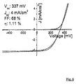
- the I/V curve of a first type of solar cell prepared with 0.1 weight percent of oxidized spiro MeO-TAD is shown in figure 6 and the corresponding parameters are shown in table 1 below.
- the radical cation salts are soluble in solutions such as chloroform, chlorobenzene, acetone and alcohol. They are deep blue or greenish blue in solution.
- the chloroform solution is stable for more than one week.
- UV spectra of hole transport material doped with various dopants were taken on a Hitachi U-3000 spectrophotometer.
- Figure 1 shows the UV spectra of pristine spiro-MeO-TAD and dopant N(PhBr) 3 SbCl 6 ) in chloroform at a concentration of 10 -5 M.
- the absorption value of dopant is found to be at 309 nm and that of spiro-MeO-TAD at 297 and 357 nm.
- the UV-Vis spectra of the spiro-MeO-TAD doped with 10 percent by weight of dopant N(PhBr) 3 SbCl 6 in chloroform at a concentration of 10 -5 M are shown in figure 2. As can be seen, there is not much shift in these absorption when the spiro compound is mixed with the dopant, but in addition to the above two strong absorption values at 297 and 357 nm, there is a new absorption at 518nm. This may be due to the formation of charge-transfer complex between the hole transport material and the dopant resulting in higher conductivity of the hole transport material due to the creation of positive centers which is responsible for the increase in the efficiency of the solar cell with the addition of the dopant.
- the new species may be a radical cation. It was observed that the color of the solution is diminishing with time and become colorless within hours. The same was observed for the other two hole transport materials also. This indicated that the new species obtained by the addition of the dopant to the hole transport material is unstable.
- Figure 2 shows the UV-Vis spectra of the spiro compound doped with the dopant N(PhBr) 3 SbCl 6 immediately after mixing (at zero hour) and after four hours. In comparison, it is clear that the absorption at 518 nm is vanished after four hours, not only that the intensity of the absorption at 377 nm is also lowered. This shows that the newly formed species is very unstable and the life time of this species is less than four hours.
- the hole transport material was chemically oxidized into a radical cation salt and then mixed with the unmodified hole transport material.
- Figure 3 show the UV-Vis spectra of pristine spiro compound, spiro compound doped with dopant N(PhBr) 3 SbCl 6 (10% by weight) and oxidized spiro compound (oxidized with AgSbF 6 ), in chloroform at a concentration of 10 -5 M.
- the similarity in absorption at 519 nm of the RCS spiro-SbF 6 - with that of the prior art doped spiro compound indicates that the species formed by the chemical oxidation is similar in nature.
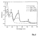
- FIG. 4 shows the UV-Vis spectra of pristine and spiro compound doped with 5 percent by weight of oxidized spiro compound at zero hour, after one day and one week. Unlike the spiro compound doped with the dopant N(PhBr) 3 SbCl 6 , only slight changes in intensity of absorption could be found after one day. The oxidized spiro compound is still stable in solution after one week.
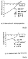
- Figure 7 proves the stability of the cells. After 6 month in air, the energy conversion efficiency of the solar cells decreases only form 0.7 % to 0.5 %. After the same period, solar cells of the prior art gave almost no V CC and J SC .
Landscapes
- Engineering & Computer Science (AREA)
- Manufacturing & Machinery (AREA)
- Hybrid Cells (AREA)
- Photovoltaic Devices (AREA)
- Electroluminescent Light Sources (AREA)
Abstract
Description
- The present invention relates to a device having a solid conjugated semiconductor, doped hole transport materials, solar cells comprising the same and methods for the preparation of such devices.
- Since the demonstration of crystalline silicon p/n junction solar cell in 1954 by Chapin et al with a reported efficiency of 6%, there was a dramatic increase in the efficiencies of such cells as a result of improvements in current, significant increase in voltage and splitting the sunlight among solar cells of different bandgaps. The higher voltages resulted directly from increasing the densities of minority carriers generated by absorbed sunlight. By reducing the minority carrier recombination rate, trapping light in active layers and by increasing the intensity of light with concentration optics, efficiencies as high as 25-30% have been reported for two band-gap single crystal laboratory cells like AlGaAs/GaAs. Thin film multijunction, multi-band-gap cells using hydrogenated amorphous silicon or polycrystalline alloys exhibit up to 15% laboratory efficiency. The efficiencies of commercial power systems in the field remain in the range of 3 to 12%.
- As an alternative a dye sensitized semiconductor-electrolyte solar cell was developed by Grätzel et al consisting of titanium dioxide nanoparticles with a ruthenium complex adsorbed on the surface of an iodine-iodide electrolyte as disclosed in WO91/16719. The ruthenium complex acts as a sensitizer, which absorbs light and injects an electron into titanium dioxide; the dye is then regenerated by electron transfer from the iodine-iodide redox couple. The advantage of such a solar cell results from the fact that no crystalline semiconductors have to be used anymore while already providing conversion efficiencies of light into electrical energy of up to 12% (O'Reagan, B. et al; Nature (1991), 353, page 737).
- However, replacement of the liquid electrolyte with solid charge transport material has been found important due to practical applications. Solid-state dye sensitized solar cells on nanoporous film of TiO2 are a significant area of research for chemists, physicists and material scientists. These researches on solar cells became very important due to its low costs and the easiness of fabrication.
- In the field of dye sensitized solid state solar cells, Hagen et al, Synethic Metals 89, 1997, 215, reports for the first time the concept of a new type of solid-state dye sensitized solar cell using organic hole transport material (HTM), which was further improved by Bach et al, Nature 398, 1998, 583, to obtain an overall conversion efficiency of 0.74%. The basic structure of the cell consists of a nanoporous TiO2 layer coated on a conducting glass substrate, covered with a compact TiO2 layer. Dye was absorbed by the nanoporous layer and the HTM along with dopant and salt was coated over the dye. The additives, salt and dopant (tris (4-bromophenyl)ammoniumyl hexachloroantimonate (N(PhBr)3SbCl6) increased the efficiency.
- Further, organic molecules with large conjugated π-system have long been known to act as semiconductors in the solid state. Conjugated semiconductors can exhibit energy bandgaps of 1eV up to several eV depending on the choice of the structure and their arrangement. However such bandgaps lead to a very low intrinsic conductivity.
- Most of the useful properties of semiconductors occur only if they are doped, depending on the application with small p- or n-type molecules. Improvements of the properties due to doping are most often related to higher conductivity resulting in a lower series resistance of the devices, to shifted adsorption edges or workfunction, to increased internal quantum efficiencies.
- Doping will allow the construction of any device traditionally made with inorganic semiconductors like silicon, including diodes, transistors and photovoltaic cells. In solid state photovoltaic cells only small molecule doping is known.
- To summarize, the specific conductivity of thin organic films is one of the most important properties that determines whether an organic semiconductor is suitable to be used in electronic devices. Conjugated semiconductors can exhibit energy bandgaps of 1eV up to several eV depending on the choice of the structure and their arrangement. Such bandgaps lead to a very low intrinsic conductivity. To improve the conductivity, organic semiconductors are doped by adding either electron acceptors (p-type) or electron donors (n-type). However, one disadvantage of many doped systems known in the prior art is their instability. For example, iodine has the tendency to diffuse out of the layer and damages electrode material. Furthermore, phase separation and degradation is a problem in known doped semiconductors, and the addition of dopants of the prior art complicates the electronic structure at the interfaces of the layers making the understanding of these solar cells difficult.
- It is therefore an object of the present invention to overcome the drawbacks of the prior art, especially to provide a device having a solid conjugated semiconductor having an increased stability compared to the respective devices known in the prior art and avoiding phase separation and degradation.
- A further object of the present invention is to provide a mixture which can be used as doped hole transport material.
- A still further object of the present invention is to provide a method for preparation of a device having a solid conjugated semiconductor, more particularly of a device exhibiting the favorable characteristics as defined above.
- This object is solved in a first aspect by a device having a solid conjugated semiconductor comprising an unmodified hole transport material, wherein the unmodified hole transport material is mixed with oxidized hole transport material as a dopant, preferably an only dopant.
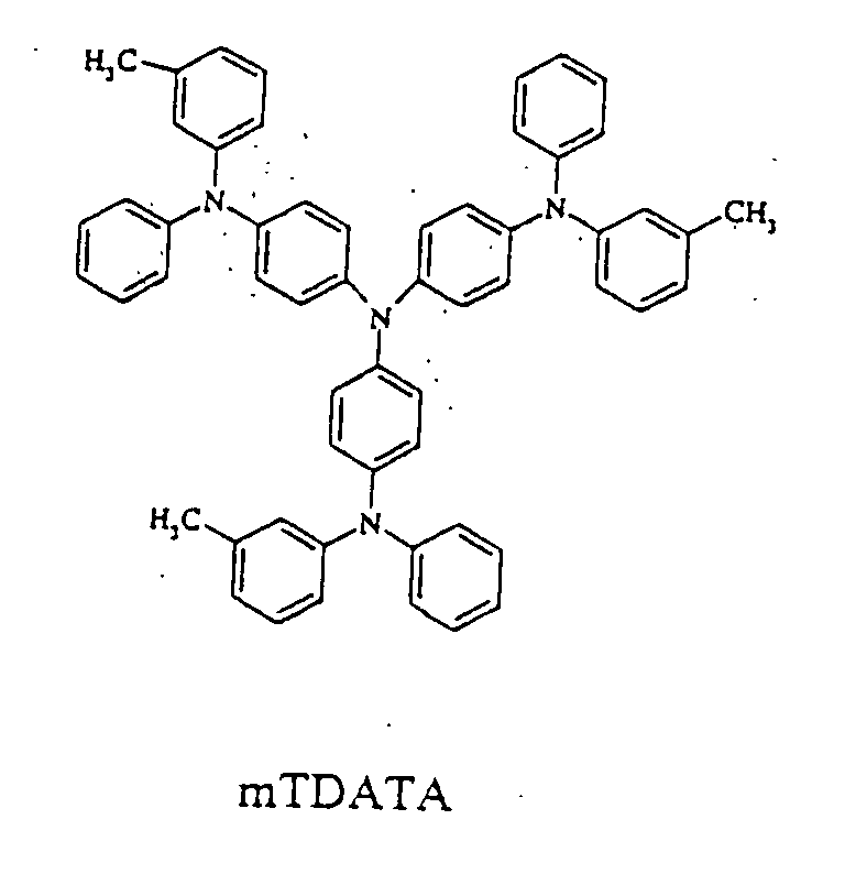
- It is preferred that the (unmodified) hole transport material is represented by formula (I)wherein R in each occurrence is dependently selected from hexyl and ethylhexyl within the wt% ratio of hexyl:ethylhexyl being about 40: about 60, or represented by formula (II)
 or represented by formula (III)
- Further, a photovoltaic device is preferred, wherein the oxidized hole transport material is present in the mixture with the unmodified hole transport material in a range of about 0.01 wt% to 10 wt%, preferably in a range of about 0.08 to 1.2 wt%.
- It is preferred that the device further comprises a semiconductor oxide layer sensitized with a dye.
- In a further embodiment the dye is a ruthenium complex.
- In another embodiment of the inventive device the semiconductor oxide layer is porous.
- In a preferred embodiment the semiconductor oxide layer comprises nanoparticles, preferably nanoparticles of TiO2.
- In a further aspect the object is solved by a mixture comprising unmodified hole transport material and oxidized hole transport material.
- In a further aspect the problem is solved by the use of the inventive mixture in any of the inventive devices, particularly as a doped hole transport material.
- In a still further aspect the problem is solved by the use of the inventive mixture for the manufacture of any of the inventive devices, particularly as a doped hole transport material.
- The problem is also solved by a method for preparing of a device having a solid conjugated semiconductor, preferably any of the inventive devices comprising the steps of:
- (i) oxidizing hole transport material;
- (ii) mixing the oxidized hole transport material with unmodified hole transport material; and
- (iii) applying the mixture to a semiconductor oxide layer.
-
- Preferred is a method, wherein the hole transport material in step (i) is chemically oxidized.
- Preferably, unreacted reactants and reduced oxidants are removed prior mixing step (ii).
- Further preferred is a method, wherein the oxidation is carried out using silver hexafluoroantimonate (AgSbF6) ornitrosonium tetrafluoroborate (NOBF4).
- Still further preferred is a method, wherein by oxidation radical cations of the hole transport material are obtained.
- In a further embodiment of the inventive method the method further comprises at least one of the following steps:
- providing a semiconductor oxide layer,
- applying said mixture to said semiconductor oxide layer, and
- connecting electrodes to said semiconductor oxide layer and to said mixture.
- In a further aspect the problem is solved by a solar cell comprising an inventive device.
- Preferred is a solar cell, wherein the solar cell is a solid state solar cell.
- Surprisingly, it was found that with the device having a solid conjugated semiconductor according to the present invention no phase separation and degradation of hole transport material and dopant occurs since they have basically the same structure. Moreover, the stability is much improved compared to the stability of prior art devices resulting in an increased energy conversion efficiency. In contrast to the prior art, no small molecules are added as dopants to the conjugated semiconductor according to the present invention, that means that no additional cation is present in the hole transport material layer. With the concept of the present invention it is possible to prepare an individual dopant for each hole transport material. The doping according to the present invention may be called "in situ" doping.
- The way of doping according to the present invention may be applied to the construction of any device made with conjugated organic and polymeric semiconductors, including diodes (LEDs), transistors, photovoltaic cells, etc..
- Besides the hole transport materials already disclosed in the application, other compounds are as well suitable and may comprise linear as well as branched or starburst structures and polymers carrying long alkoxy groups as sidechains or in the backbone. Such hole transport materials are in principle disclosed in
EP 0 901 175 A2, the disclosure of which is incorporated herein by reference. - Other possible hole transport materials are, e.g. described in the WO 98/48433, DE 19704031.4 and DE 19735270.7. The latter two references disclose TDAB for application in organic LEDs. It is to be noted that any of the known TDAB may be - further- derivatized such as by using substitutions such as alkoxy, alkyl, silyl at the end-standing phenyl rings which could be in p-, m- and o-position mono-, bi-, or tri-substituted. As indicated already above the guidelines disclosed herein apply not only to single organic hole transport materials but also to mixtures thereof.
- Dyes which can be used for sensitizing a semiconductor oxide layer are known in the art such as
EP 0 887 817 A2 the disclosure of which is incorporated herein by reference. Among the dyes to be used are also Ru(II) dyes. - The dyes used to sensitize the semiconductor oxide layer may be attached thereto by chemisorption, adsorption or by any other suitable ways.
- The semiconductor oxide layer used in the inventive device is preferably a nanoparticulate one. The material can be a metal oxide and more preferably an oxide of the transition metals or of the elements of the third main group, the fourth, fifth and sixth subgroup of the periodic system. These and any other suitable materials are known to those skilled in the art and are, e.g. disclosed in
EP 0 333 641 A1, the disclosure of which is incorporated herein by reference. - The semiconductor oxide layer material may exhibit a porous structure. Due to this porosity the surface area is increased which allows for a bigger amount of sensitizing dye to be immobilized on the semiconductor oxide layer and thus for an increased performance of the device. Additionally, the rough surface allows the trapping of light which is reflected from the surface and directed to neighbouring surface which in turn increases the yield of the light.
- The method for the manufacture of a device according to the present invention can be exemplary summarized as follows.
- I. Structuring of TCO (transparent conductive oxide layer) substrates
- II. Cleaning of TCO substrates
- a. Ultrasonic cleaning 15 minutes in an aqueous surfactant at ca. 70°C
- b. Rinse thoroughly with ultrapure water and dry in air
- c. Ultrasonic rinsing with ultrapure water 15 min at ca. 70°C
- d. Ultrasonic cleaning 15 minutes in pure isopropanol at ca. 70°C
- e. Blow dry with nitrogen
- III. Preparation of blocking layer
- a. Making polycrystalline TiO2 by spray pyrolysis of titanium acetylacetonate solution.
- b. Temper film at 500°C.
- IV. Preparation of nanoporous TiO2 semiconductor oxide layer
- a. Screen printing: use a TiO2 paste with a screen structured with the desired geometry (thickness depends on screen mesh); resulting standard thickness is about 3 µm; doctor blading is an alternative technique to make porous TiO2 layer
- b. Sintering of film
- 1. Heat the substrates up to 85°C for 30 minutes to dry the film
- 2. Sinter at 450°C for ½ hour, ideally under oxygen flow, otherwise in air
- 3. Let sample cool down slowly to avoid cracking
- V. Dyeing of nanocrystalline TiO2 semiconductor oxide film
- a. Prepare a solution of dye in ethanol, concentration ca. 5 x 10⁻⁴ M
- b. Put the ca. 80°C warm substrates into the dye solution.
- c. Let them sit in the dye-solution at room temperature in the dark for about 8 hours or overnight.
- d. Remove from dye solution, rinse with ethanol and let dry several hours or overnight in the dark.
- VI. Deposition of hole transport material
- a. Prepare a solution of HTM. Current "standard conditions" are:
- Solvent: chlorobenzene (plus ca. 10 % acetonitrile from dopant solution)
- HTM: concentration (5 - 60 mg/substrate)
- Dopant: oxidized HTM (ca. 0,2 mol% of hole conductor concentration, to be added from a solution in acetonitrile)
- Salt: Li((CF3SO2)2N), (ca. 9 mol%)
- b. Spin-coat the solution onto the film
- c. Let the samples dry at least several hours in air or preferably overnight
- VII. Deposition of counterelectrode
- a. Evaporate the counterelectrode on top (currently Au)
-
- As is understood changes may be done in that method without departing from the scope of protection.
- The invention is now further illustrated by the accompanying figures from which further embodiments, features and advantages may be taken and where
- Figure 1
- is a UV-Vis spectra of dopant N(PhBr)3SbCl6 and spiro-MeO-TAD in chloroform at a concentration of 10-5M;
- Figure 2
- is a UV-Vis spectra of spiro-MeO-TAD doped with dopant N(PhBr)3SbCl6 (10% by weight) in chloroform at a concentration of 10-5M at 0 hour and after 4 hours;
- Figure 3
- is a UV-Vis spectra of pristine spiro-MeO-TAD, spiro doped with dopant N(PhBr)3SbCl6 (10 % by weight) and oxidized spiro in chloroform at a concentration of 10-5 M;
- Figure 4
- is a UV-Vis spectra of pristine spiro-MeO-TAD and sprio doped with oxidized spiro (5% by weight) in chloroform at a concentration of 10-5M at 0 hour after one day and after one week.
- Figure 5
- shows the basic design of the inventive solar cell;
- Figure 6
- shows the I/V curve of a first type of solar cell prepared with 0.1 wt% of oxidized spiro MeO-TAD (light source:sulphur lamp, white light 100 mW/cm2, measured withpower meter at 530 nm); and
- Figure 7
- shows the long term stability of the inventive solid solar cell over a period of 6
months.
- a) I/V-characteristic after preparation (light source: Oriel 75W Xenon arc lamp, white light 100 mW/cm2 (measured with a power-meter at 550 nm);
- b) I/V-characteristic after 6 month (light source: Oriel 150 W Xenon arc lamp, AM 1,5 global, (calibration with Si-photodiode: 80 mW/cm2)).
- Materials: three different hole transport materials were used, 2,2',7,7'-tetrakis(diphenylamino)-9,9'-spirofluorene (spiro-MeO-TAD) and m-trimethyl-diphenylaminotriamine (mTDATA) are commercially available by Covlon and SynTec, respectively. The third hole transport material, TDAB is a mixture of tris(methoxyphenyl hexyloxy phenyl amino) benzene (MH-TDAB) and tris(methoxyphenyl ethylhexyloxy phenyl amino) benzene (MEH-TDAB), prepared according to literature. The solvents used were freshly distilled and dried under argon atmosphere. The materials silver hexafluoroantimonate and nitrosonium tetrafluoroborate (Aldrich) were used as received.
- Radical cations salts were prepared with two different anions, namely SbF6 - anion and BF4 - anion.
- 0.49g (0.0004mol) of spiro-MeO-TAD was dissolved in 70 ml toluene under argon atmosphere. To this, 0.5g (0.0016mol) of silver hexafluoroantimonate dissolved in 40ml toluene was added under argon atmosphere. The mixture was allowed to stir at room temerature for 30 minutes, the dark green solid was filtered out, washed with toluene to remove the unreacted reactants and dried in vacuum. It was then dissolved in chloroform, filtered to remove the silver. The product was reprecipitated from ether. This was repeated for three times. The product was dried in vacuum to yield 0.380g of RCS spiro-SbF6 -.
- The same procedure was used as in example 1 above with 0.49g (0.0004mol) spiro MeO-TAD and 0.1869g (0.0016mol) nitrosonium tetrafluoroborate, yielding 0.420g of the desired product.
- The procedure was the same as used in example 1 above but using 0.4076g (0.0004mol) TDAB in 30ml toluene and 0.1402g (0.0012mol) nitrosonium tetrafluoroborate in 40ml toluene, yielding 0.120g of RCS TDAB BF4 -.
- The procedure was the same as for example 1 above but using 0.789g (0.001mol) mTDATA in 30ml toluene and 1.3745g (0.004mol) silver hexafluoroantimonate in 40ml toluene yielding 1.12g of the desired product.
- Hybrid solar cells according to the present invention have the basic structure given in figure 5.
- The I/V curve of a first type of solar cell prepared with 0.1 weight percent of oxidized spiro MeO-TAD is shown in figure 6 and the corresponding parameters are shown in table 1 below.
dopant VOC[mV] JSC[mA/cm2] FF[%] η[%] 0.1 w% 337 4.0 68 1.11 - The radical cation salts (RCS) are soluble in solutions such as chloroform, chlorobenzene, acetone and alcohol. They are deep blue or greenish blue in solution. The chloroform solution is stable for more than one week.
- To compare the stability of the doped hole transport system according to the present invention with system known in the prior art, UV spectra of hole transport material doped with various dopants were taken on a Hitachi U-3000 spectrophotometer.
- Figure 1 shows the UV spectra of pristine spiro-MeO-TAD and dopant N(PhBr)3SbCl6) in chloroform at a concentration of 10-5M. The absorption value of dopant is found to be at 309 nm and that of spiro-MeO-TAD at 297 and 357 nm.
- The UV-Vis spectra of the spiro-MeO-TAD doped with 10 percent by weight of dopant N(PhBr)3SbCl6 in chloroform at a concentration of 10-5 M are shown in figure 2. As can be seen, there is not much shift in these absorption when the spiro compound is mixed with the dopant, but in addition to the above two strong absorption values at 297 and 357 nm, there is a new absorption at 518nm. This may be due to the formation of charge-transfer complex between the hole transport material and the dopant resulting in higher conductivity of the hole transport material due to the creation of positive centers which is responsible for the increase in the efficiency of the solar cell with the addition of the dopant. The new species may be a radical cation. It was observed that the color of the solution is diminishing with time and become colorless within hours. The same was observed for the other two hole transport materials also. This indicated that the new species obtained by the addition of the dopant to the hole transport material is unstable. Figure 2 shows the UV-Vis spectra of the spiro compound doped with the dopant N(PhBr)3SbCl6 immediately after mixing (at zero hour) and after four hours. In comparison, it is clear that the absorption at 518 nm is vanished after four hours, not only that the intensity of the absorption at 377 nm is also lowered. This shows that the newly formed species is very unstable and the life time of this species is less than four hours. To make the system stable, it is therefor necessary to have stable material, which has the similar structure and physical properties of the hole transport material. To achieve this, the hole transport material was chemically oxidized into a radical cation salt and then mixed with the unmodified hole transport material.
- Figure 3 show the UV-Vis spectra of pristine spiro compound, spiro compound doped with dopant N(PhBr)3SbCl6 (10% by weight) and oxidized spiro compound (oxidized with AgSbF6), in chloroform at a concentration of 10-5M. The similarity in absorption at 519 nm of the RCS spiro-SbF6 - with that of the prior art doped spiro compound indicates that the species formed by the chemical oxidation is similar in nature. In addition, there are two more new absorption at 677 and 887 nm found for the oxidized spiro compound.
- To show the stability of the oxidized spiro compound, UV-Vis spectra were measured at different intervals. Figure 4 shows the UV-Vis spectra of pristine and spiro compound doped with 5 percent by weight of oxidized spiro compound at zero hour, after one day and one week. Unlike the spiro compound doped with the dopant N(PhBr)3SbCl6, only slight changes in intensity of absorption could be found after one day. The oxidized spiro compound is still stable in solution after one week. This clearly indicates that the radical cation of the spiro compound obtained by chemical oxidation leads to a doped conjugated semiconductor, which shows improved characteristics compared to the doped conjugated semiconductors known in the prior art, and therefore to an improved device having improved stability and no phase separation and degradation.
- Figure 7 proves the stability of the cells. After 6 month in air, the energy conversion efficiency of the solar cells decreases only form 0.7 % to 0.5 %. After the same period, solar cells of the prior art gave almost no VCC and JSC.
- The features of the present invention disclosed in the description, the claims and/or the drawings may both separately and in any combination thereof be material for realizing the invention in various forms thereof.
Claims (18)
- Device having a solid conjugated semiconductor comprising an unmodified hole transport material, wherein the hole transport material is mixed with oxidized hole transport material as a dopant.
- Device according to claim 1 wherein the hole transport material is represented by formula (I)wherein R in each occurrence is dependently selected from hexyl and ethylhexyl within the wt% ratio of hexyl:ethylhexyl being about 40: about 60, or represented by formula (II)
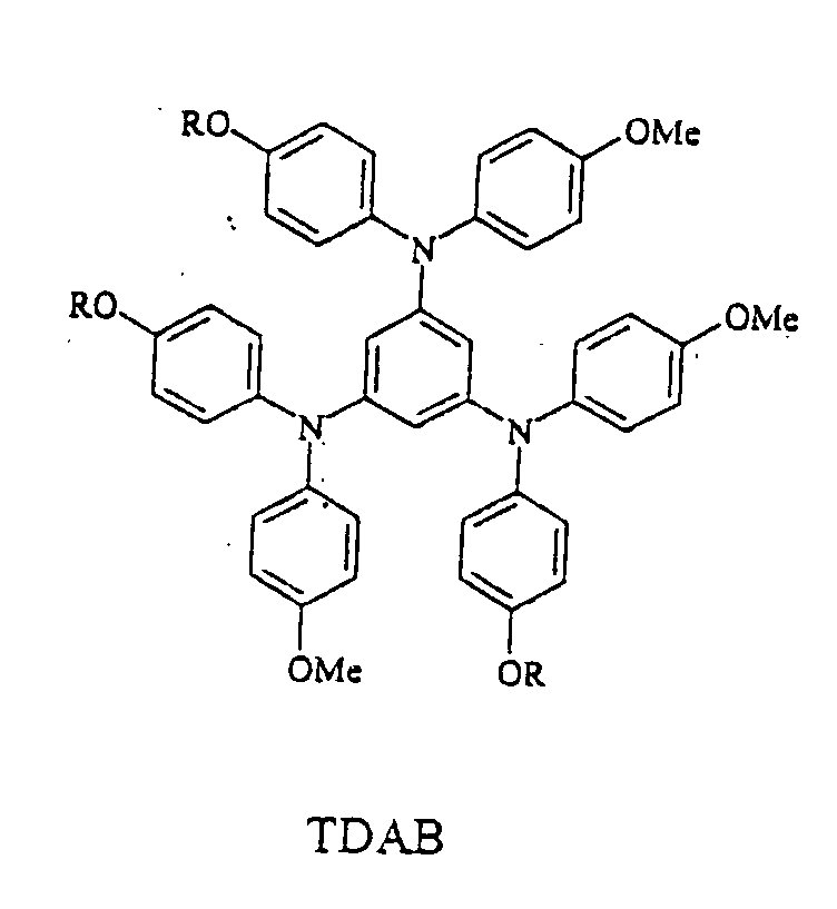 or represented by formula (III)

- Device according to claim 1 or 2, wherein the oxidized hole transport material is present in the mixture with the hole transport material in a range of about 0.01 wt% to 10 wt%, preferably in a range of about 0.08 to 1.2 wt%.
- Device according to any of the preceding claims, wherein the device further comprises a semiconductor oxide layer sensitized with a dye.
- Device according claim 4, wherein the dye is a ruthenium complex.
- Device according to any of the preceding claims wherein the semiconductor oxide layer is porous.
- Device according to claim 6, wherein the semiconductor oxide layer comprises nanoparticles, preferably nanoparticles of TiO2.
- Mixture comprising hole transport material and oxidized hole transport material.
- Use of the mixture according to claim 8 in a device according to any of claims 1 to 7, particularly as a doped hole transport material.
- Use of the mixture according to claim 8 for the manufacture of a device according to any of claims 1 to 7, particularly as a doped hole transport material.
- Method for preparing of a device having a solid conjugated semiconductor, preferably a device according to any of the claims 1 to 7, comprising the steps of:(i) oxidizing hole transport material;(ii) mixing the oxidized hole transport material with hole transport material; and(iii) applying the mixture to a semiconductor oxide layer.
- Method according to claim 11, wherein the hole transport material in step (i) is chemically oxidized.
- Method according to claim 12, wherein unreacted reactants and reduced oxidants are removed prior mixing step (ii).
- Method according to claim 13, wherein the oxidation is carried out using silver hexafluoroantimonate (AgSbF6) or nitrosonium tetrafluoroborate (NOBF4).
- Method according to any of claims 11-14, wherein by oxidation radical cations of the hole transport material are obtained.
- Method according to any of claims 11 to 15, wherein the method further comprises at least one of the following steps:(i) providing a semiconductor oxide layer,(ii) applying said mixture to said semiconductor oxide layer, and(iii) connecting electrodes to said semiconductor oxide layer and to said mixture.
- Solar cell comprising a device according to any of the claims 1 to 7.
- Solar cell according to claim 17, wherein the solar cell is a solid state solar cell.
Priority Applications (5)
| Application Number | Priority Date | Filing Date | Title |
|---|---|---|---|
| EP01121179A EP1289030A1 (en) | 2001-09-04 | 2001-09-04 | Doping of a hole transporting material |
| AU2002300570A AU2002300570B2 (en) | 2001-09-04 | 2002-08-15 | Photovoltaic Device and Method for Preparing the Same |
| US10/234,543 US7061009B2 (en) | 2001-09-04 | 2002-09-03 | Solid conjugated semiconductor device having an unmodified hole transport material |
| JP2002259245A JP2003197942A (en) | 2001-09-04 | 2002-09-04 | Photovoltaic device and manufacturing method thereof |
| KR1020020053267A KR20030020856A (en) | 2001-09-04 | 2002-09-04 | Device having a solid conjugated semiconductor and method for preparing the same |
Applications Claiming Priority (1)
| Application Number | Priority Date | Filing Date | Title |
|---|---|---|---|
| EP01121179A EP1289030A1 (en) | 2001-09-04 | 2001-09-04 | Doping of a hole transporting material |
Publications (1)
| Publication Number | Publication Date |
|---|---|
| EP1289030A1 true EP1289030A1 (en) | 2003-03-05 |
Family
ID=8178541
Family Applications (1)
| Application Number | Title | Priority Date | Filing Date |
|---|---|---|---|
| EP01121179A Ceased EP1289030A1 (en) | 2001-09-04 | 2001-09-04 | Doping of a hole transporting material |
Country Status (5)
| Country | Link |
|---|---|
| US (1) | US7061009B2 (en) |
| EP (1) | EP1289030A1 (en) |
| JP (1) | JP2003197942A (en) |
| KR (1) | KR20030020856A (en) |
| AU (1) | AU2002300570B2 (en) |
Cited By (6)
| Publication number | Priority date | Publication date | Assignee | Title |
|---|---|---|---|---|
| WO2008154915A1 (en) * | 2007-06-20 | 2008-12-24 | Osram Opto Semiconductors Gmbh | Use of a metal complex as a p-dopant for an organic semiconductive matrix material, organic semiconductor material, and electronic component |
| WO2008154914A1 (en) * | 2007-06-20 | 2008-12-24 | Osram Opto Semiconductors Gmbh | Use of a metal complex as a p-dopant for an organic semiconductive matrix material, organic semiconductor material, and organic light-emitting diodes |
| WO2008155310A1 (en) * | 2007-06-20 | 2008-12-24 | Siemens Aktiengesellschaft | Semiconductor material and organic rectifier diode |
| US8034466B2 (en) | 2004-12-06 | 2011-10-11 | Semiconductor Energy Laboratory Co., Ltd. | Light-emitting element and light-emitting device using the same |
| CN104144908A (en) * | 2013-01-22 | 2014-11-12 | 中国科学院理化技术研究所 | Spirofluorene derivative molecular glass and its preparation method and application in photolithography |
| US9818944B2 (en) | 2013-05-30 | 2017-11-14 | Oxford University Innovation Limited | Organic semiconductor doping process |
Families Citing this family (25)
| Publication number | Priority date | Publication date | Assignee | Title |
|---|---|---|---|---|
| AT410729B (en) * | 2000-04-27 | 2003-07-25 | Qsel Quantum Solar Energy Linz | PHOTOVOLTAIC CELL WITH A PHOTOACTIVE LAYER OF TWO MOLECULAR ORGANIC COMPONENTS |
| AT411306B (en) * | 2000-04-27 | 2003-11-25 | Qsel Quantum Solar Energy Linz | PHOTOVOLTAIC CELL WITH A PHOTOACTIVE LAYER OF TWO MOLECULAR ORGANIC COMPONENTS |
| AT410859B (en) * | 2000-04-27 | 2003-08-25 | Qsel Quantum Solar Energy Linz | METHOD FOR PRODUCING A PHOTOVOLTAIC CELL WITH A PHOTOACTIVE LAYER FROM TWO ORGANIC COMPONENTS |
| DE60132450T2 (en) * | 2001-09-04 | 2008-04-17 | Sony Deutschland Gmbh | Solar cell and manufacturing method |
| JP4967211B2 (en) * | 2001-09-26 | 2012-07-04 | 日本電気株式会社 | Photoelectrochemical device |
| JP2006516819A (en) * | 2003-01-30 | 2006-07-06 | ユニバーシティ・オブ・ケープ・タウン | Thin film semiconductor device and manufacturing method of thin film semiconductor device |
| JP4243237B2 (en) * | 2003-11-10 | 2009-03-25 | 淳二 城戸 | Organic element, organic EL element, organic solar cell, organic FET structure, and organic element manufacturing method |
| KR100882172B1 (en) | 2004-03-11 | 2009-02-06 | 미쓰비시 가가꾸 가부시키가이샤 | Composition and ion compound for charge transport film, charge transport film and organic electroluminescent device using same, method for manufacturing organic electroluminescent device and method for manufacturing charge transport film |
| EP1837927A1 (en) * | 2006-03-22 | 2007-09-26 | Novaled AG | Use of heterocyclic radicals for doping of organic semiconductors |
| WO2010009234A1 (en) | 2008-07-16 | 2010-01-21 | Wisconsin Alumni Research Foundation | Metal substrates including metal oxide nanoporous thin films and methods of making the same |
| US8779126B2 (en) | 2008-10-29 | 2014-07-15 | Fujifilm Corporation | Dye, photoelectric conversion element using the same, photoelectrochemical cell, and method of producing dye |
| JP5524557B2 (en) | 2009-09-28 | 2014-06-18 | 富士フイルム株式会社 | Method for producing photoelectric conversion element, photoelectric conversion element, and photoelectrochemical cell |
| JP5620081B2 (en) | 2009-09-28 | 2014-11-05 | 富士フイルム株式会社 | Method for manufacturing photoelectric conversion element |
| KR101596918B1 (en) * | 2009-12-11 | 2016-02-23 | 고려대학교 산학협력단 | Solid State Polymeric Electrolytes Containing Hole Transporting Moieties for Low-Cost Dye-Sensitized Solar Cell Applications |
| KR20140007416A (en) * | 2011-02-01 | 2014-01-17 | 바스프 에스이 | Photovoltaic element |
| US20130125968A1 (en) * | 2011-11-18 | 2013-05-23 | Sunpreme, Ltd. | Low-cost solar cell metallization over tco and methods of their fabrication |
| GB201208793D0 (en) * | 2012-05-18 | 2012-07-04 | Isis Innovation | Optoelectronic device |
| JP5972811B2 (en) | 2013-02-22 | 2016-08-17 | 富士フイルム株式会社 | Photoelectric conversion element, method for producing photoelectric conversion element, and dye-sensitized solar cell |
| CN105593206B (en) * | 2013-10-02 | 2017-10-10 | 默克专利有限公司 | Hole mobile material |
| BR112017028382B1 (en) * | 2015-07-30 | 2022-08-16 | Sekisui Chemical Co., Ltd | SOLAR CELL AND ORGANIC SEMICONDUCTOR MATERIAL |
| JP6380694B2 (en) | 2016-03-24 | 2018-08-29 | 三菱ケミカル株式会社 | Electron-accepting compound, charge transport film composition, and light-emitting device using the same |
| CN110534648B (en) * | 2019-08-30 | 2021-10-08 | 华中科技大学 | A kind of organic small molecule halide modified perovskite photoelectric functional material, its preparation and application |
| JP7550399B2 (en) * | 2020-04-17 | 2024-09-13 | 国立大学法人 東京大学 | Dopants and Conductor Materials |
| EP4144802A4 (en) * | 2020-05-01 | 2024-07-10 | The University of Tokyo | CONDUCTOR MATERIAL |
| CN116686423A (en) * | 2021-02-10 | 2023-09-01 | 高峰 | Preparation method of device transport material composition, composition, transport layer comprising same, and electronic device comprising transport layer |
Citations (2)
| Publication number | Priority date | Publication date | Assignee | Title |
|---|---|---|---|---|
| US4338222A (en) * | 1980-04-11 | 1982-07-06 | Xerox Corporation | Semiconductive organic compositions |
| DE19711713A1 (en) * | 1997-03-20 | 1998-10-01 | Hoechst Ag | Photovoltaic cell |
Family Cites Families (12)
| Publication number | Priority date | Publication date | Assignee | Title |
|---|---|---|---|---|
| JP2937015B2 (en) * | 1993-07-28 | 1999-08-23 | 住友電気工業株式会社 | Organic electroluminescence device |
| US5804322A (en) * | 1995-11-17 | 1998-09-08 | Motorola, Inc. | Organic electroluminescence device with mixed hole transporting materials |
| US5943154A (en) * | 1996-09-17 | 1999-08-24 | Kabushiki Kaisha Toshiba | Optically-controlled light control element |
| JP3911066B2 (en) * | 1997-02-17 | 2007-05-09 | 新日本製鐵株式会社 | Organic electroluminescence device |
| SE509440C2 (en) * | 1997-05-14 | 1999-01-25 | Tetra Laval Holdings & Finance | Methods of preparing a color-ink-packed packaging material, especially for aseptic packaging, and packaging containers thereof |
| US5853906A (en) * | 1997-10-14 | 1998-12-29 | Xerox Corporation | Conductive polymer compositions and processes thereof |
| US6171765B1 (en) * | 1998-05-26 | 2001-01-09 | Agilent Technologies, Inc. | Photolithographic processing for polymer LEDs with reactive metal cathodes |
| JP2001094130A (en) * | 1999-09-21 | 2001-04-06 | Fuji Photo Film Co Ltd | Photoelectric conversion device, solar cell and novel oligopyrrole compound |
| SG98433A1 (en) * | 1999-12-21 | 2003-09-19 | Ciba Sc Holding Ag | Iodonium salts as latent acid donors |
| US6340528B1 (en) * | 2000-01-19 | 2002-01-22 | Xerox Corporation | Crosslinkable polymer compositions for donor roll coatings |
| EP1160888A1 (en) * | 2000-05-29 | 2001-12-05 | Sony International (Europe) GmbH | Hole transporting agents and photoelectric conversion device comprising the same |
| JP2003068469A (en) * | 2000-08-11 | 2003-03-07 | Canon Inc | Organic electroluminescence device and method of manufacturing the same |
-
2001
- 2001-09-04 EP EP01121179A patent/EP1289030A1/en not_active Ceased
-
2002
- 2002-08-15 AU AU2002300570A patent/AU2002300570B2/en not_active Ceased
- 2002-09-03 US US10/234,543 patent/US7061009B2/en not_active Expired - Fee Related
- 2002-09-04 KR KR1020020053267A patent/KR20030020856A/en not_active Ceased
- 2002-09-04 JP JP2002259245A patent/JP2003197942A/en not_active Withdrawn
Patent Citations (2)
| Publication number | Priority date | Publication date | Assignee | Title |
|---|---|---|---|---|
| US4338222A (en) * | 1980-04-11 | 1982-07-06 | Xerox Corporation | Semiconductive organic compositions |
| DE19711713A1 (en) * | 1997-03-20 | 1998-10-01 | Hoechst Ag | Photovoltaic cell |
Non-Patent Citations (1)
| Title |
|---|
| AASMUNDVEIT K E ET AL: "STRUCTURAL ASPECTS OF ELECTROCHEMICAL DOPING AND DEDOPING OF POLY(3,4-ETHYLENEDIOXYTHIOPHENE)", SYNTHETIC METALS, ELSEVIER SEQUOIA, LAUSANNE, CH, vol. 113, no. 1/2, 15 June 2000 (2000-06-15), pages 93 - 97, XP000961516, ISSN: 0379-6779 * |
Cited By (16)
| Publication number | Priority date | Publication date | Assignee | Title |
|---|---|---|---|---|
| US8034466B2 (en) | 2004-12-06 | 2011-10-11 | Semiconductor Energy Laboratory Co., Ltd. | Light-emitting element and light-emitting device using the same |
| EP3157073A1 (en) * | 2007-06-20 | 2017-04-19 | OSRAM OLED GmbH | Use of a metal complex as a p-dopant for an organic semiconductive matrix material, organic semiconductor material, and organic light-emitting diode |
| KR20160088940A (en) * | 2007-06-20 | 2016-07-26 | 오스람 오엘이디 게엠베하 | Use of a metal complex as a p-dopant for an organic semiconductive matrix material, organic semiconductor material, and organic light-emitting diodes |
| WO2008154914A1 (en) * | 2007-06-20 | 2008-12-24 | Osram Opto Semiconductors Gmbh | Use of a metal complex as a p-dopant for an organic semiconductive matrix material, organic semiconductor material, and organic light-emitting diodes |
| US8278652B2 (en) | 2007-06-20 | 2012-10-02 | Siemens Aktiengesellschaft | Semiconductor material for an organic diode |
| US8513702B2 (en) | 2007-06-20 | 2013-08-20 | Osram Opto Semiconductors Gmbh | Use of a metal complex as a p-dopant for an organic semiconductive matrix material, organic semiconductor material and organic light-emitting diodes |
| CN101730945B (en) * | 2007-06-20 | 2013-12-25 | 西门子公司 | Semiconductor material and organic rectifier diode |
| WO2008155310A1 (en) * | 2007-06-20 | 2008-12-24 | Siemens Aktiengesellschaft | Semiconductor material and organic rectifier diode |
| TWI483440B (en) * | 2007-06-20 | 2015-05-01 | Siemens Ag | Semiconductor materials and organic rectifier diodes |
| CN101785127B (en) * | 2007-06-20 | 2014-03-26 | 奥斯兰姆奥普托半导体有限责任公司 | Use of a metal complex as a p-dopant for an organic semiconductive matrix material, organic semiconductor material, and organic light-emitting diodes |
| EP3157072A1 (en) * | 2007-06-20 | 2017-04-19 | OSRAM OLED GmbH | Use of a metal complex as a p-dopant for an organic semiconductive matrix material, organic semiconductor material, and organic light-emitting diode |
| WO2008154915A1 (en) * | 2007-06-20 | 2008-12-24 | Osram Opto Semiconductors Gmbh | Use of a metal complex as a p-dopant for an organic semiconductive matrix material, organic semiconductor material, and electronic component |
| CN104144908A (en) * | 2013-01-22 | 2014-11-12 | 中国科学院理化技术研究所 | Spirofluorene derivative molecular glass and its preparation method and application in photolithography |
| CN104144908B (en) * | 2013-01-22 | 2016-02-03 | 中国科学院理化技术研究所 | Spirofluorene derivative molecular glass and its preparation method and application in photolithography |
| US9818944B2 (en) | 2013-05-30 | 2017-11-14 | Oxford University Innovation Limited | Organic semiconductor doping process |
| US9929343B2 (en) | 2013-05-30 | 2018-03-27 | Oxford University Innovation Limited | Organic semiconductor doping process |
Also Published As
| Publication number | Publication date |
|---|---|
| US7061009B2 (en) | 2006-06-13 |
| JP2003197942A (en) | 2003-07-11 |
| US20030067000A1 (en) | 2003-04-10 |
| KR20030020856A (en) | 2003-03-10 |
| AU2002300570B2 (en) | 2007-01-18 |
| AU2002300570C1 (en) | 2003-06-12 |
Similar Documents
| Publication | Publication Date | Title |
|---|---|---|
| US7061009B2 (en) | Solid conjugated semiconductor device having an unmodified hole transport material | |
| EP1289028B1 (en) | Photovoltaic device and method for preparing the same | |
| Albero et al. | Influence of the composition of hybrid perovskites on their performance in solar cells | |
| US7943848B2 (en) | Photoelectric conversion element, method of manufacturing the same and solar cell | |
| US7947898B2 (en) | Photoelectric conversion element and solar cell | |
| KR101740654B1 (en) | Organic/inorganic hybrid perovskite compound, preparing method thereof, and solar cell comprising the same | |
| KR20010110117A (en) | Hole transporting agents and photoelectric conversion device comprising the same | |
| JP5206092B2 (en) | Photoelectric conversion element and solar cell | |
| EP3518301A1 (en) | Crystal defects mitigating agents for high power conversion efficiency and stability of perovskite photovoltaic devices | |
| US8039741B2 (en) | Photoelectric conversion element and solar cell | |
| KR20170107766A (en) | Solar cell and preparation method thereof | |
| JP5347329B2 (en) | Photoelectric conversion element and solar cell | |
| CN116686423A (en) | Preparation method of device transport material composition, composition, transport layer comprising same, and electronic device comprising transport layer | |
| US20150279572A1 (en) | Solid-state dye-densitized solar cell with long-term stability containing pyridine-based additive | |
| JP5332114B2 (en) | Photoelectric conversion element and solar cell | |
| JP2010282780A (en) | Photoelectric conversion element and solar cell | |
| JP2008226582A (en) | Photoelectric conversion element and solar cell | |
| KR102869355B1 (en) | Inorganic semiconductor quantum dots substituted with pyridine ligands, Quantumdot solar cell comprising the same, and manufacturing method of the quantumdot solar cell | |
| JP2010009830A (en) | Photoelectric conversion element and its manufacturing method as well as solar cell | |
| JP5250989B2 (en) | Photoelectric conversion element and solar cell | |
| JP2010040280A (en) | Photoelectric conversion element and solar cell | |
| JP2009218093A (en) | Photoelectric conversion element, and solar cell | |
| JP2010251180A (en) | Photoelectric conversion element and solar cell | |
| JP2010282779A (en) | Dye-sensitized photoelectric conversion element and solar cell | |
| JP2011086481A (en) | Photoelectric conversion element and solar cell |
Legal Events
| Date | Code | Title | Description |
|---|---|---|---|
| PUAI | Public reference made under article 153(3) epc to a published international application that has entered the european phase |
Free format text: ORIGINAL CODE: 0009012 |
|
| AK | Designated contracting states |
Kind code of ref document: A1 Designated state(s): AT BE CH CY DE DK ES FI FR GB GR IE IT LI LU MC NL PT SE TR Designated state(s): AT BE CH CY DE DK ES FI FR GB GR IE IT LI LU MC NL PT SE TR |
|
| AX | Request for extension of the european patent |
Extension state: AL LT LV MK RO SI |
|
| 17P | Request for examination filed |
Effective date: 20030327 |
|
| AKX | Designation fees paid |
Designated state(s): DE FR GB NL |
|
| RIN1 | Information on inventor provided before grant (corrected) |
Inventor name: KARICKAL, RAMAN HARIDSA, Inventor name: THELAKKAT, MUKUNDAN Inventor name: SCHMIDT, HANS-WERNER Inventor name: GAERING, STEPHANE Inventor name: YASUDA, AKIO,SONY INTERNATIONAL (EUROPE) GMBH Inventor name: NELLES, GABRIELE,SONY INTERNATIONAL (EUROPE) GMBH |
|
| RAP1 | Party data changed (applicant data changed or rights of an application transferred) |
Owner name: SONY DEUTSCHLAND GMBH |
|
| RAP1 | Party data changed (applicant data changed or rights of an application transferred) |
Owner name: SONY DEUTSCHLAND GMBH |
|
| STAA | Information on the status of an ep patent application or granted ep patent |
Free format text: STATUS: THE APPLICATION HAS BEEN REFUSED |
|
| 18R | Application refused |
Effective date: 20070206 |