EP1288335A1 - Surface-coated carbide alloy cutting tool - Google Patents
Surface-coated carbide alloy cutting tool Download PDFInfo
- Publication number
- EP1288335A1 EP1288335A1 EP02019362A EP02019362A EP1288335A1 EP 1288335 A1 EP1288335 A1 EP 1288335A1 EP 02019362 A EP02019362 A EP 02019362A EP 02019362 A EP02019362 A EP 02019362A EP 1288335 A1 EP1288335 A1 EP 1288335A1
- Authority
- EP
- European Patent Office
- Prior art keywords
- layer
- cemented carbide
- average thickness
- coated cemented
- cutting tool
- Prior art date
- Legal status (The legal status is an assumption and is not a legal conclusion. Google has not performed a legal analysis and makes no representation as to the accuracy of the status listed.)
- Granted
Links
Images


Classifications
-
- C—CHEMISTRY; METALLURGY
- C23—COATING METALLIC MATERIAL; COATING MATERIAL WITH METALLIC MATERIAL; CHEMICAL SURFACE TREATMENT; DIFFUSION TREATMENT OF METALLIC MATERIAL; COATING BY VACUUM EVAPORATION, BY SPUTTERING, BY ION IMPLANTATION OR BY CHEMICAL VAPOUR DEPOSITION, IN GENERAL; INHIBITING CORROSION OF METALLIC MATERIAL OR INCRUSTATION IN GENERAL
- C23C—COATING METALLIC MATERIAL; COATING MATERIAL WITH METALLIC MATERIAL; SURFACE TREATMENT OF METALLIC MATERIAL BY DIFFUSION INTO THE SURFACE, BY CHEMICAL CONVERSION OR SUBSTITUTION; COATING BY VACUUM EVAPORATION, BY SPUTTERING, BY ION IMPLANTATION OR BY CHEMICAL VAPOUR DEPOSITION, IN GENERAL
- C23C16/00—Chemical coating by decomposition of gaseous compounds, without leaving reaction products of surface material in the coating, i.e. chemical vapour deposition [CVD] processes
- C23C16/22—Chemical coating by decomposition of gaseous compounds, without leaving reaction products of surface material in the coating, i.e. chemical vapour deposition [CVD] processes characterised by the deposition of inorganic material, other than metallic material
- C23C16/30—Deposition of compounds, mixtures or solid solutions, e.g. borides, carbides, nitrides
- C23C16/40—Oxides
- C23C16/403—Oxides of aluminium, magnesium or beryllium
-
- C—CHEMISTRY; METALLURGY
- C23—COATING METALLIC MATERIAL; COATING MATERIAL WITH METALLIC MATERIAL; CHEMICAL SURFACE TREATMENT; DIFFUSION TREATMENT OF METALLIC MATERIAL; COATING BY VACUUM EVAPORATION, BY SPUTTERING, BY ION IMPLANTATION OR BY CHEMICAL VAPOUR DEPOSITION, IN GENERAL; INHIBITING CORROSION OF METALLIC MATERIAL OR INCRUSTATION IN GENERAL
- C23C—COATING METALLIC MATERIAL; COATING MATERIAL WITH METALLIC MATERIAL; SURFACE TREATMENT OF METALLIC MATERIAL BY DIFFUSION INTO THE SURFACE, BY CHEMICAL CONVERSION OR SUBSTITUTION; COATING BY VACUUM EVAPORATION, BY SPUTTERING, BY ION IMPLANTATION OR BY CHEMICAL VAPOUR DEPOSITION, IN GENERAL
- C23C16/00—Chemical coating by decomposition of gaseous compounds, without leaving reaction products of surface material in the coating, i.e. chemical vapour deposition [CVD] processes
- C23C16/56—After-treatment
-
- C—CHEMISTRY; METALLURGY
- C23—COATING METALLIC MATERIAL; COATING MATERIAL WITH METALLIC MATERIAL; CHEMICAL SURFACE TREATMENT; DIFFUSION TREATMENT OF METALLIC MATERIAL; COATING BY VACUUM EVAPORATION, BY SPUTTERING, BY ION IMPLANTATION OR BY CHEMICAL VAPOUR DEPOSITION, IN GENERAL; INHIBITING CORROSION OF METALLIC MATERIAL OR INCRUSTATION IN GENERAL
- C23C—COATING METALLIC MATERIAL; COATING MATERIAL WITH METALLIC MATERIAL; SURFACE TREATMENT OF METALLIC MATERIAL BY DIFFUSION INTO THE SURFACE, BY CHEMICAL CONVERSION OR SUBSTITUTION; COATING BY VACUUM EVAPORATION, BY SPUTTERING, BY ION IMPLANTATION OR BY CHEMICAL VAPOUR DEPOSITION, IN GENERAL
- C23C30/00—Coating with metallic material characterised only by the composition of the metallic material, i.e. not characterised by the coating process
- C23C30/005—Coating with metallic material characterised only by the composition of the metallic material, i.e. not characterised by the coating process on hard metal substrates
-
- Y—GENERAL TAGGING OF NEW TECHNOLOGICAL DEVELOPMENTS; GENERAL TAGGING OF CROSS-SECTIONAL TECHNOLOGIES SPANNING OVER SEVERAL SECTIONS OF THE IPC; TECHNICAL SUBJECTS COVERED BY FORMER USPC CROSS-REFERENCE ART COLLECTIONS [XRACs] AND DIGESTS
- Y10—TECHNICAL SUBJECTS COVERED BY FORMER USPC
- Y10T—TECHNICAL SUBJECTS COVERED BY FORMER US CLASSIFICATION
- Y10T407/00—Cutters, for shaping
- Y10T407/27—Cutters, for shaping comprising tool of specific chemical composition
-
- Y—GENERAL TAGGING OF NEW TECHNOLOGICAL DEVELOPMENTS; GENERAL TAGGING OF CROSS-SECTIONAL TECHNOLOGIES SPANNING OVER SEVERAL SECTIONS OF THE IPC; TECHNICAL SUBJECTS COVERED BY FORMER USPC CROSS-REFERENCE ART COLLECTIONS [XRACs] AND DIGESTS
- Y10—TECHNICAL SUBJECTS COVERED BY FORMER USPC
- Y10T—TECHNICAL SUBJECTS COVERED BY FORMER US CLASSIFICATION
- Y10T428/00—Stock material or miscellaneous articles
- Y10T428/24—Structurally defined web or sheet [e.g., overall dimension, etc.]
- Y10T428/24942—Structurally defined web or sheet [e.g., overall dimension, etc.] including components having same physical characteristic in differing degree
- Y10T428/2495—Thickness [relative or absolute]
- Y10T428/24967—Absolute thicknesses specified
- Y10T428/24975—No layer or component greater than 5 mils thick
-
- Y—GENERAL TAGGING OF NEW TECHNOLOGICAL DEVELOPMENTS; GENERAL TAGGING OF CROSS-SECTIONAL TECHNOLOGIES SPANNING OVER SEVERAL SECTIONS OF THE IPC; TECHNICAL SUBJECTS COVERED BY FORMER USPC CROSS-REFERENCE ART COLLECTIONS [XRACs] AND DIGESTS
- Y10—TECHNICAL SUBJECTS COVERED BY FORMER USPC
- Y10T—TECHNICAL SUBJECTS COVERED BY FORMER US CLASSIFICATION
- Y10T428/00—Stock material or miscellaneous articles
- Y10T428/26—Web or sheet containing structurally defined element or component, the element or component having a specified physical dimension
- Y10T428/263—Coating layer not in excess of 5 mils thick or equivalent
- Y10T428/264—Up to 3 mils
- Y10T428/265—1 mil or less
-
- Y—GENERAL TAGGING OF NEW TECHNOLOGICAL DEVELOPMENTS; GENERAL TAGGING OF CROSS-SECTIONAL TECHNOLOGIES SPANNING OVER SEVERAL SECTIONS OF THE IPC; TECHNICAL SUBJECTS COVERED BY FORMER USPC CROSS-REFERENCE ART COLLECTIONS [XRACs] AND DIGESTS
- Y10—TECHNICAL SUBJECTS COVERED BY FORMER USPC
- Y10T—TECHNICAL SUBJECTS COVERED BY FORMER US CLASSIFICATION
- Y10T428/00—Stock material or miscellaneous articles
- Y10T428/30—Self-sustaining carbon mass or layer with impregnant or other layer
-
- Y—GENERAL TAGGING OF NEW TECHNOLOGICAL DEVELOPMENTS; GENERAL TAGGING OF CROSS-SECTIONAL TECHNOLOGIES SPANNING OVER SEVERAL SECTIONS OF THE IPC; TECHNICAL SUBJECTS COVERED BY FORMER USPC CROSS-REFERENCE ART COLLECTIONS [XRACs] AND DIGESTS
- Y10—TECHNICAL SUBJECTS COVERED BY FORMER USPC
- Y10T—TECHNICAL SUBJECTS COVERED BY FORMER US CLASSIFICATION
- Y10T83/00—Cutting
- Y10T83/929—Tool or tool with support
Definitions
- the Ti compound layer as a lower layer, is formed on the surface of a cemented carbide substrate under normal deposition conditions and an Al 2 O 3 layer having a ⁇ - or ⁇ -type crystal structure is formed also under normal deposition conditions and then the resulting material is subjected to a heat treatment in this state, preferably, in an Ar atmosphere under the conditions of a temperature of 1000°C or higher for a predetermined time, the ⁇ - or ⁇ -type crystal structure is converted into an ⁇ -crystal structure.
- the Al 2 O 3 layer having the heat transformed ⁇ -type crystal structure preferably has a structure in which cracks formed during the heat transformation are uniformly dispersed and distributed.
- the Ti compound layer itself has the toughness (strength) and the hard coating layer is provided with the toughness by the presence of the Ti compound layer, and also strongly adheres to any of the cemented carbide substrate and the heat transformed ⁇ -type Al 2 O 3 as the intermediate layer, thereby to exert an effect of contributing to an improvement in adhesion to the cemented carbide substrate of the hard coating layer.
- the average thickness is less than 0.5 ⁇ m, the effect described above cannot be sufficiently exerted.
- the thickness exceeds 20 ⁇ m chipping is liable to occur at the cutting edge portion. Therefore, the average thickness of this layer is preferably within a range from 0.5 to 20 ⁇ m.
- the upper layer has a function of sufficiently entering into cracks formed during the heat transformation at the interface with the heat transformed ⁇ -type Al 2 O 3 layer, thereby making it possible to maintain the cracks formed during the heat transformation in a markedly stable state.
- the average thickness is less than 0.3 ⁇ m, the function described above cannot be sufficiently exerted.
- the average thickness is up to 10 ⁇ m, the function can be sufficiently exerted. Therefore, the average thickness of this layer is preferably within a range from 0.3 to 10 ⁇ m.
- the Ti oxide layer has very low affinity for steel and cast iron and also has a characteristic wherein chips produced during cutting are less likely to be smeared, that is, there is surface lubricity. Consequently, abnormal damage caused by smeared chips is markedly suppressed. This effect is particularly exerted when workpieces having a high viscosity made of stainless steel and mild steel are cut.
- a ratio of a peak intensity of (006) plane, I(006), to a peak intensity of (012) plane, I(012), is preferably 0.1 or more in an X-ray diffraction profile of the ⁇ -type aluminum oxide layer which constitutes the hard coating layer.
- the heat transformed ⁇ -type Al 2 O 3 layer is preferably formed in the following manner. First, in order to stably form a ⁇ - or ⁇ -type crystal structure without including an ⁇ -type component, an Al 2 O 3 layer is formed under the conditions of a temperature of 1000°C or less, preferably 970°C or less, and more preferably 950°C or less.
- Fig. 1 is an X-ray diffraction chart of the coated cemented carbide tool 17 of the present invention.
- Fig. 2 is an X-ray diffraction chart of the conventional cemented carbide tool 17.
- coated cemented carbide tool of the present invention will be explained by way of embodiments.
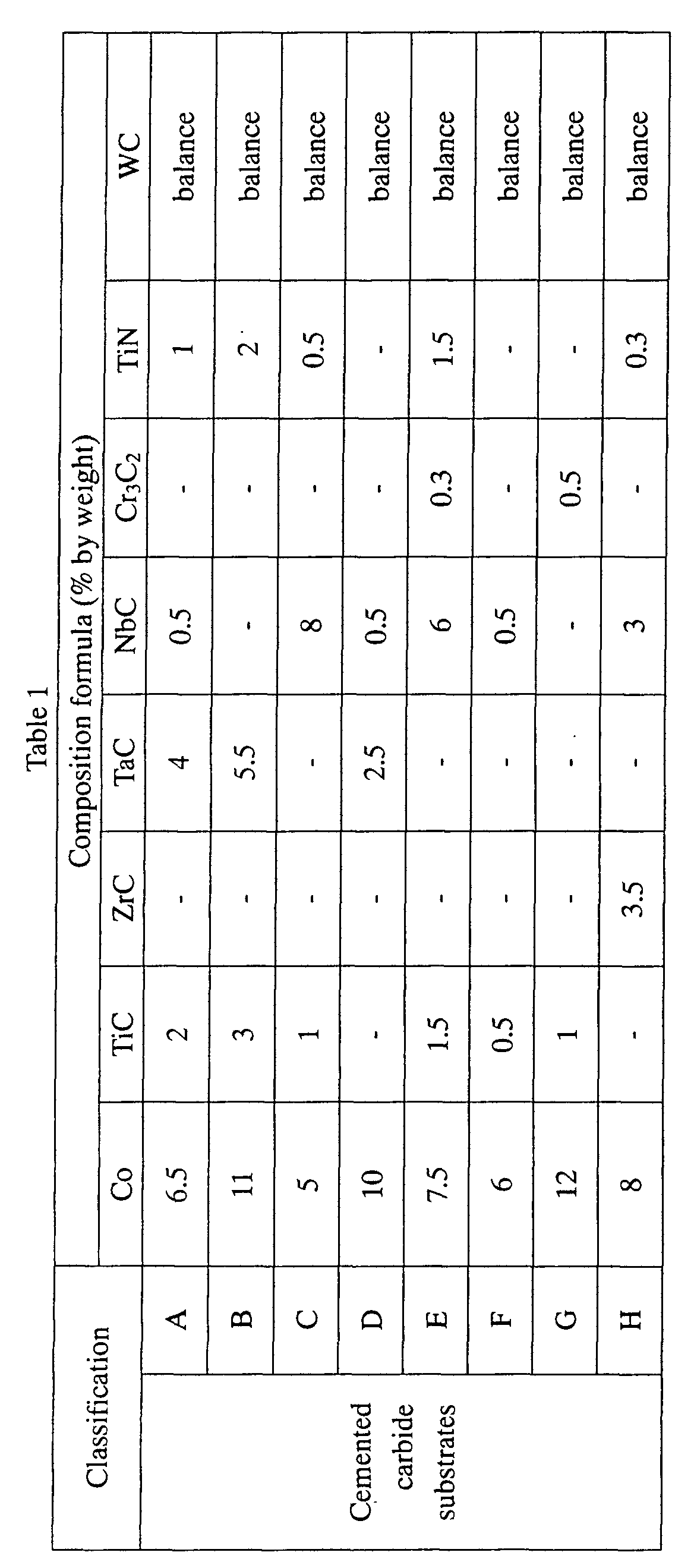
- Cemented carbide substrates A to H each having a shape of a insert defined in ISO CNMG120412 were produced by preparing a WC powder, a TiC powder, a ZrC powder, a TaC powder, a NbC powder, a Cr 3 C 2 powder, a TiN powder and a Co powder each having a predetermined average grain size of 1 to 5 ⁇ m as raw powders, compounding these raw powders according to each formulation shown in Table 1, further adding a wax, mixing them in ethanol in a ball mill for 24 hours, drying the mixture, compacting the dried mixture under a pressure of 150 MPa to form green compacts, vacuum-sintering these green compacts under the conditions of a vacuum degree of 5 Pa and a predetermined temperature within a range from 1370 to 1470°C for one hour, and subjecting the cutting edge portion to honing (R: 0.07 mm) after it was cooled to room termperature.
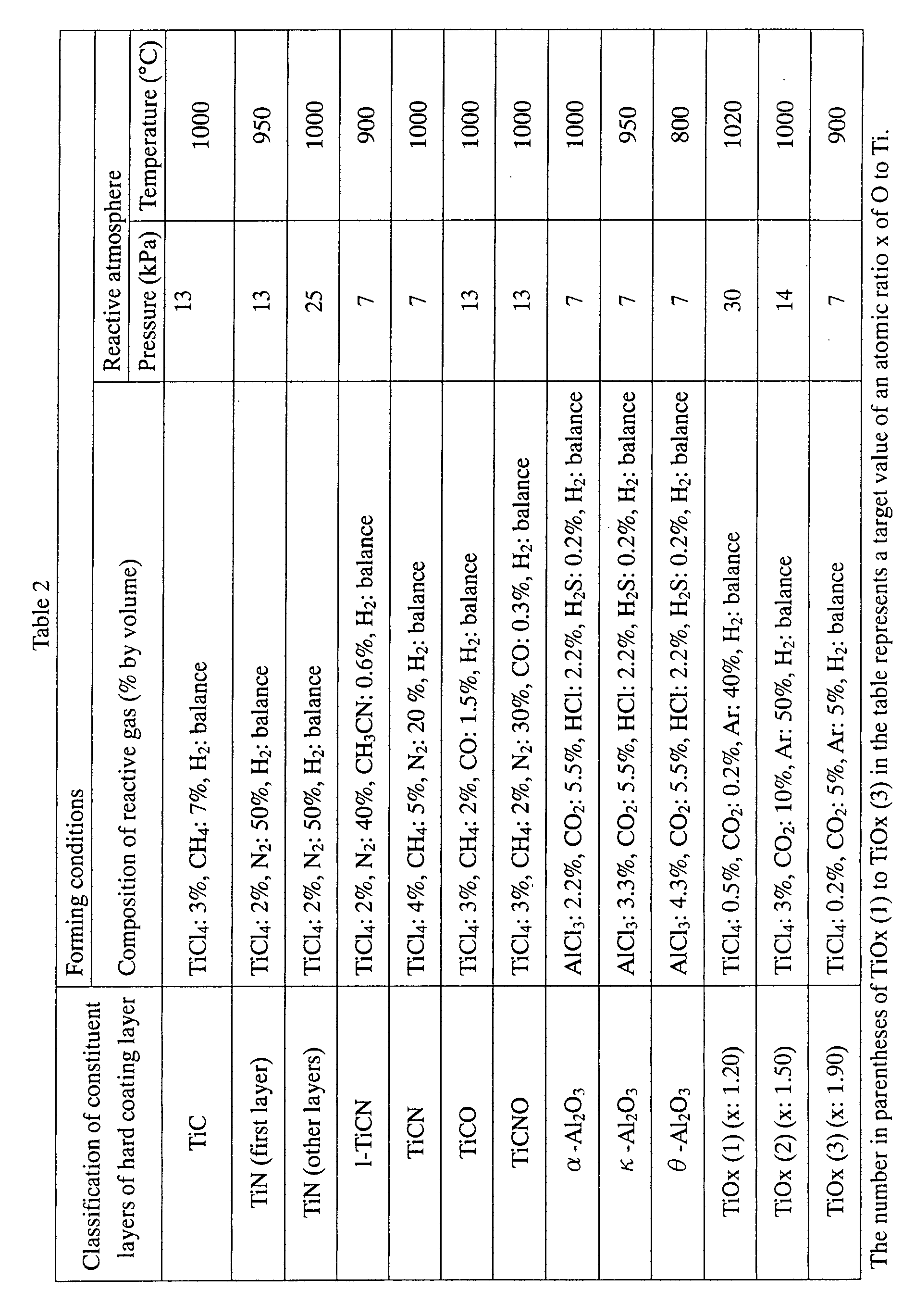
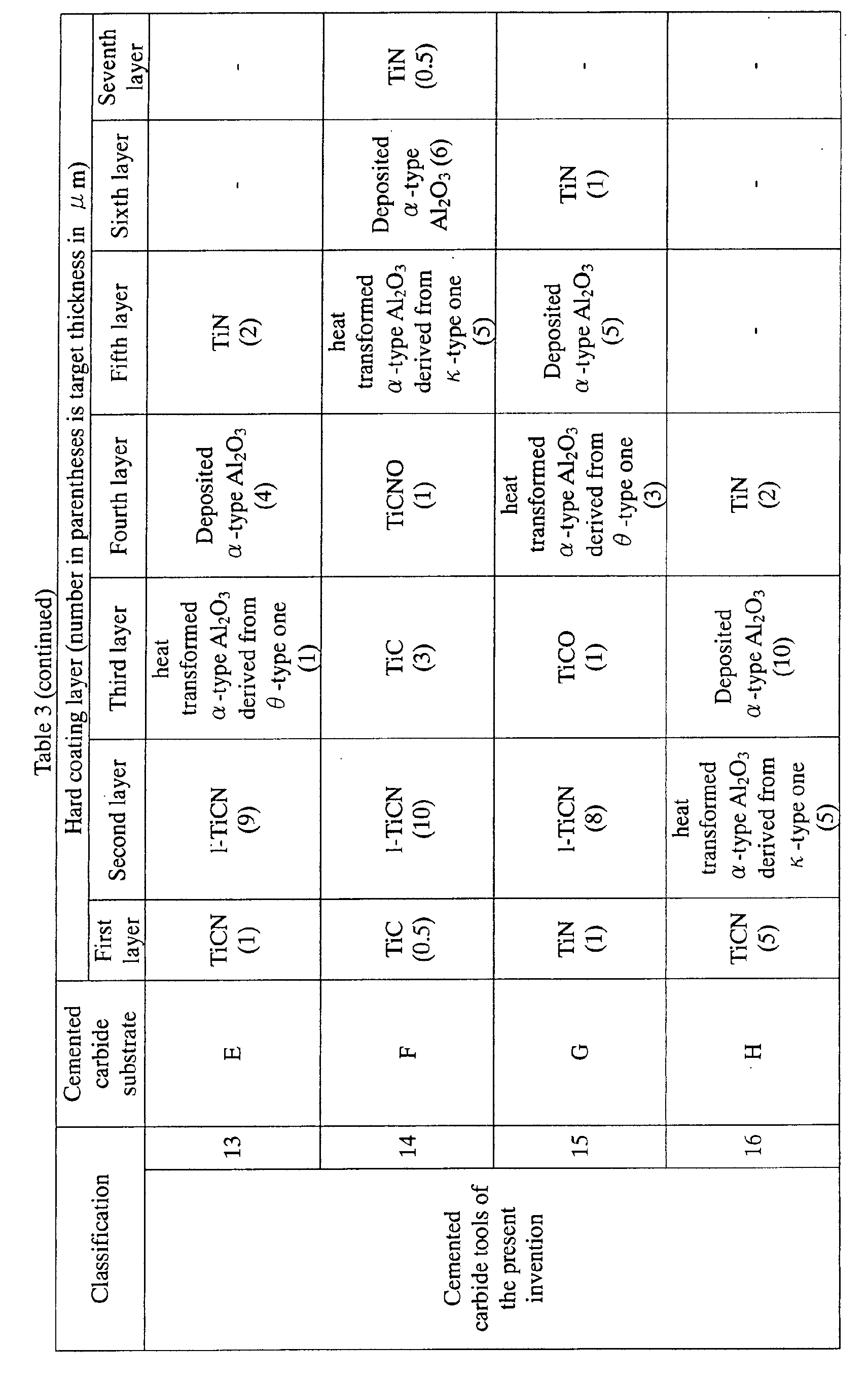
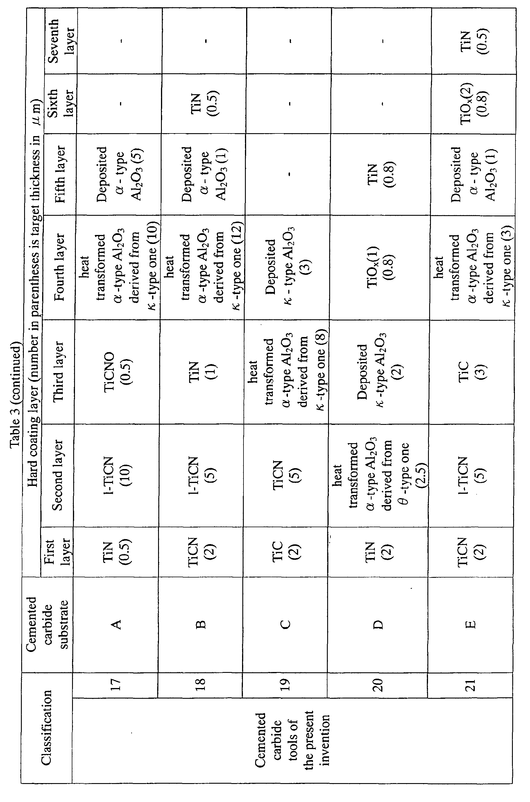
- Hei 6-8008) shown in Table 2 using a conventional CVD apparatus, and as an intermediate layer of the hard coating layer, an Al 2 O 3 layer having a ⁇ - or ⁇ -type crystal structure and a target thickness shown in Table 3 was first formed thereon under the conditions shown in Table 2, and then the ⁇ - or ⁇ -type crystal structure was converted into an ⁇ -type crystal structure wherein cracks formed during the heat transformation are uniformly dispersed and distributed in the layer by subjecting it to a subsequent heat treatment in an Ar atmosphere under the conditions of a temperature of 1050°C for 1 to 8 hours.
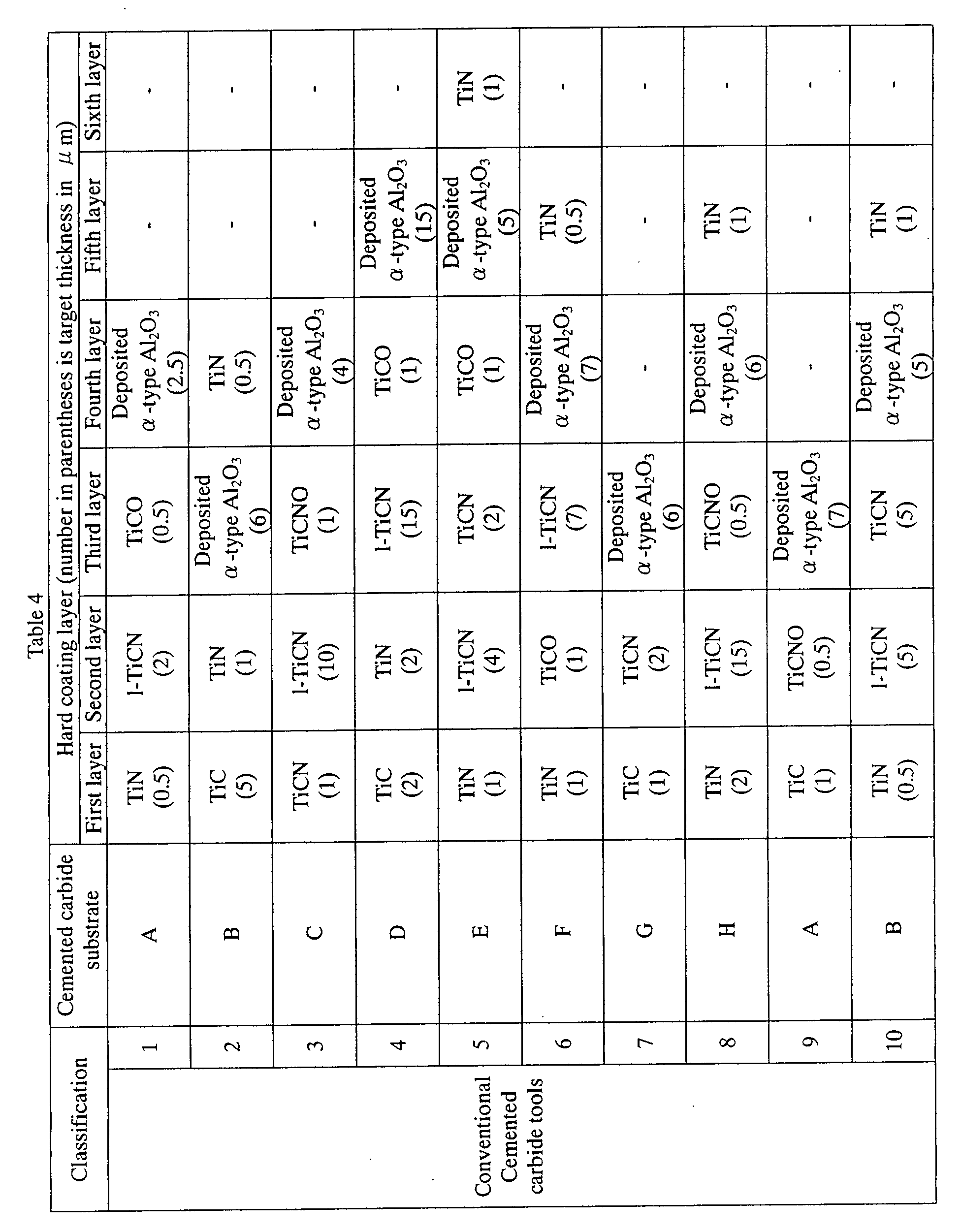
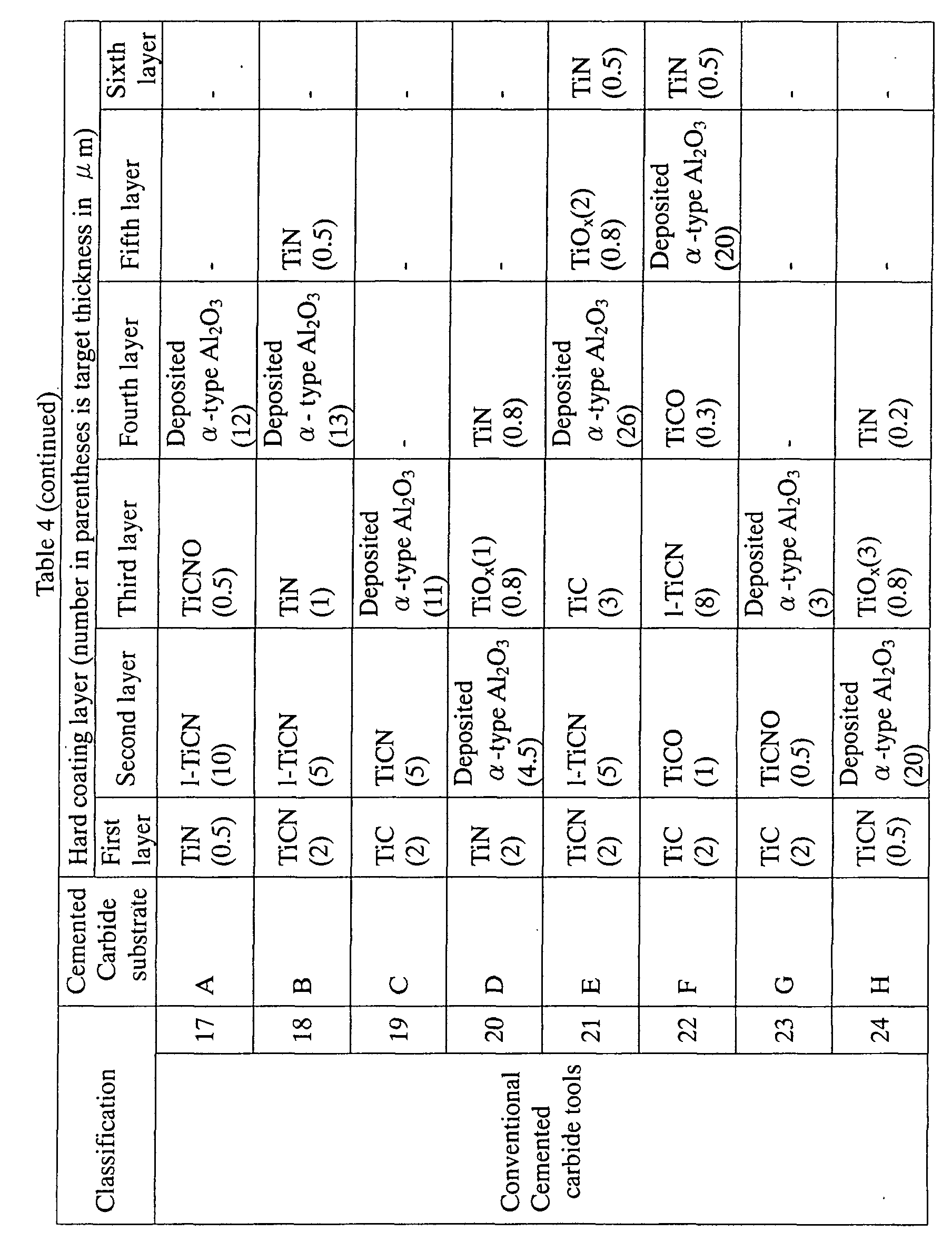
- each hard coating layer of any of the former coated cemented carbide tools is composed of a Ti compound layer, a heat transformed ⁇ -type Al 2 O 3 layer wherein cracks formed during the heat transformation are uniformly dispersed and distributed in the layer and an as-deposited ⁇ -type Al 2 O 3 layer and, if necessary, a TiN layer
- each hard coating layer of any of the latter coated cemented carbide tools is composed of a Ti compound layer and an as-deposited ⁇ -type Al 2 O 3 layer and, if necessary, a TiN layer.
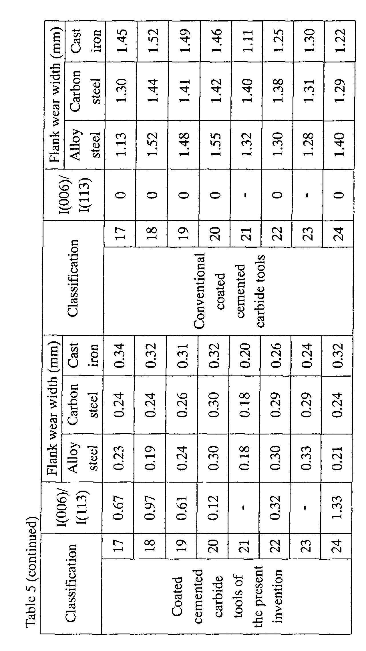
- the cemented carbide tool of the present invention is preferably composed of the Al 2 O 3 having a value of 0.1 or more. Since ⁇ -type Al 2 O 3 wherein basal plane of the unit cell of the respective crystals apt to exhibit a characteristic orientation, which is generally in parallel with the film growth surface, was transformed into ⁇ -type Al 2 O 3 , said peak ratio becomes 0.1 or more when the thickness is 4 ⁇ m or more. Said peak ratio is particularly preferably 0.5 or more.
- all coated cemented carbide tools 1 to 24 of the present invention exhibit excellent wear resistance because the cutting edge portion has an excellent thermoplastic deformation resistance due to the action of cracks formed during the thermal transformation which are uniformly dispersed and distributed in a heat transformed a- type Al 2 O 3 layer constituting an intermediate layer of a hard coating layer even in a high-speed interrupted cutting test and a high-speed continuous cutting test of steel and cast iron accompanied with very high heat generation and, therefore, the cutting edge portion exhibits a normal wear pattern.
- thermoplastic deformation which can cause abnormal wear at the cutting edge portion, occurred in the high-speed cutting test, thereby accelerating the advance of wear.
Landscapes
- Chemical & Material Sciences (AREA)
- Chemical Kinetics & Catalysis (AREA)
- Engineering & Computer Science (AREA)
- Materials Engineering (AREA)
- Mechanical Engineering (AREA)
- Metallurgy (AREA)
- Organic Chemistry (AREA)
- General Chemical & Material Sciences (AREA)
- Inorganic Chemistry (AREA)
- Cutting Tools, Boring Holders, And Turrets (AREA)
- Chemical Vapour Deposition (AREA)
- Physical Vapour Deposition (AREA)
Abstract
Description





Claims (7)
- A surface-coated cemented carbide alloy cutting tool comprising a hard coating layer and a cemented carbide alloy substrate, the hard coating layer comprising:a Ti compound layer, as a lower layer, formed by vapor deposition having an average thickness of 0.5 to 20 µm and comprising at least one layer chosen from among a layer of a carbide of Ti, a layer of a nitride of Ti, a layer of a carbonitride of Ti, a layer of a carboxide of Ti, and a layer of a carbonitroxide of Ti;an aluminum oxide layer, as an intermediate layer, having an average thickness of 1 to 25 µm and having a heat transformed α-type crystal structure derived from a vapor deposited κ - or -type aluminum oxide layer; andan aluminum oxide layer, as an upper layer, formed by vapor deposition having an average thickness of 0.3 to 10 µm and having an α-type crystal structure.
- A surface-coated cemented carbide alloy cutting tool according to claim 1, wherein the hard coating layer further comprising at least one layer of titanium nitride, titanium carbide or titanium carbonitride as a surface layer formed as the uppermost layer and which has an average thickness of 0.1 to 5 µm.
- A surface-coated cemented carbide alloy cutting tool according to claim 2, further comprising a Ti oxide layer, which has an average thickness of 0.2 to 5 µm and satisfies the formula: TiOx (provided that an atomic ratio x of O to Ti is within a range from 1.2 to 1.9) as measured by an Auger electron spectroscoopy at the center portion in the thickness direction, provided between an upper layer and the surface layer.
- A surface-coated cemented carbide alloy cutting tool according to any one of claims 1 to 3, wherein a ratio of a peak intensity of (006) plane, I(006), to a peak intensity of (113) plane, I(113), is 0.1 or more in an X-ray diffraction profile of the α-type aluminum oxide layer of the hard coating layer.
- A surface-coated cemented carbide alloy cutting tool according to claim 4, wherein a ratio of a peak intensity of (006) plane, I(006), to a peak intensity of (012) plane, I(012), is 0.1 or more in an X-ray diffraction profile of the α-type aluminum oxide layer of the hard coating layer.
- A surface-coated cemented carbide alloy cutting tool according to claim 1, wherein the aluminum oxide layer has a heat transformed α-type crystal structure and has cracks therein formed during heat transformation.
- A surface-coated cemented carbide alloy cutting tool according to claim 1, wherein the aluminum oxide layer has a heat transformed α-type crystal structure and has cracks therein formed during heat transformation which are uniformly dispersed.
Applications Claiming Priority (4)
| Application Number | Priority Date | Filing Date | Title |
|---|---|---|---|
| JP2001264101 | 2001-08-31 | ||
| JP2001264101A JP2003071609A (en) | 2001-08-31 | 2001-08-31 | Surface-coated cemented carbide cutting tool that demonstrates excellent heat-resistant plastic deformability by high-speed cutting |
| JP2002189604 | 2002-06-28 | ||
| JP2002189604 | 2002-06-28 |
Publications (3)
| Publication Number | Publication Date |
|---|---|
| EP1288335A1 true EP1288335A1 (en) | 2003-03-05 |
| EP1288335B1 EP1288335B1 (en) | 2010-05-05 |
| EP1288335B2 EP1288335B2 (en) | 2013-10-02 |
Family
ID=26621429
Family Applications (1)
| Application Number | Title | Priority Date | Filing Date |
|---|---|---|---|
| EP20020019362 Expired - Lifetime EP1288335B2 (en) | 2001-08-31 | 2002-08-29 | Surface-coated carbide alloy cutting tool |
Country Status (5)
| Country | Link |
|---|---|
| US (2) | US6733874B2 (en) |
| EP (1) | EP1288335B2 (en) |
| CN (1) | CN1258420C (en) |
| AT (1) | ATE466971T1 (en) |
| DE (1) | DE60236241D1 (en) |
Cited By (12)
| Publication number | Priority date | Publication date | Assignee | Title |
|---|---|---|---|---|
| EP1348779A1 (en) * | 2002-03-22 | 2003-10-01 | Sandvik Aktiebolag | Coated cutting tool for turning of steel |
| EP1493845A1 (en) * | 2003-06-16 | 2005-01-05 | Seco Tools Ab | CVD coated cutting tool insert |
| JP2005279914A (en) * | 2003-12-22 | 2005-10-13 | Mitsubishi Materials Corp | Surface coated cermet cutting tool with excellent chipping resistance with hard coating layer |
| JP2005279913A (en) * | 2003-12-22 | 2005-10-13 | Mitsubishi Materials Corp | Surface coated cermet cutting tool with excellent chipping resistance with hard coating layer |
| JP2005279912A (en) * | 2003-12-22 | 2005-10-13 | Mitsubishi Materials Corp | Surface coated cermet cutting tool with excellent chipping resistance with hard coating layer |
| EP1528125A3 (en) * | 2003-10-27 | 2006-01-25 | Seco Tools Ab | Coated cutting insert for rough turning |
| EP1536041A3 (en) * | 2003-11-25 | 2006-03-29 | Mitsubishi Materials Corporation | Coated cermet cutting tool with a chipping resistant, hard coating layer |
| EP1479791A3 (en) * | 2003-02-28 | 2006-06-21 | Mitsubishi Materials Corporation | Cutting tool |
| EP1905870A2 (en) | 2006-09-27 | 2008-04-02 | Seco Tools Ab | Alumina layer with enhanced texture |
| US8343620B2 (en) | 2007-02-01 | 2013-01-01 | Seco Tools Ab | Alumina coated grade |
| KR20140109857A (en) * | 2011-12-26 | 2014-09-16 | 미쓰비시 마테리알 가부시키가이샤 | Surface-coated cutting tool with hard coating that exhibits excellent chipping resistance and abrasion resistance |
| EP2459771B1 (en) | 2009-07-27 | 2017-08-16 | Seco Tools Ab | Coated cutting tool insert for turning of steels |
Families Citing this family (29)
| Publication number | Priority date | Publication date | Assignee | Title |
|---|---|---|---|---|
| JP3811089B2 (en) * | 2002-04-15 | 2006-08-16 | 株式会社東芝 | Wear amount measurement method |
| SE526567C2 (en) * | 2003-07-16 | 2005-10-11 | Sandvik Intellectual Property | Support bar for long hole drill with wear surface in different color |
| JP2005131730A (en) * | 2003-10-30 | 2005-05-26 | Mitsubishi Materials Corp | Surface coated cermet cutting tool with excellent chipping resistance with hard coating layer |
| US7273665B2 (en) * | 2003-12-22 | 2007-09-25 | Mitsubishi Materials Corporation | Surface-coated cermet cutting tool with hard coating layer having excellent chipping resistance |
| SE528107C2 (en) * | 2004-10-04 | 2006-09-05 | Sandvik Intellectual Property | Coated carbide inserts, especially useful for high-speed machining of metallic workpieces |
| SE528929C2 (en) * | 2005-04-18 | 2007-03-20 | Sandvik Intellectual Property | Cut coated with a layer system and method of making this |
| SE529051C2 (en) * | 2005-09-27 | 2007-04-17 | Seco Tools Ab | Cutting tool inserts coated with alumina |
| CN101312927B (en) * | 2005-11-17 | 2011-04-06 | 倍锐特有限责任公司 | Laminated hard alloy piece |
| AT503050B1 (en) * | 2005-11-17 | 2007-09-15 | Boehlerit Gmbh & Co Kg | Coating a tool with titanium, zirconium, hafnium, vanadium, niobium, tantalum or chromium carbonitride by chemical vapor deposition comprises increasing the temperature during deposition |
| MX2008012236A (en) * | 2006-03-28 | 2009-02-10 | Sumitomo Metal Ind | Cutting tool and process for manufacturing the same. |
| WO2008082020A1 (en) * | 2007-01-02 | 2008-07-10 | Taegutec Ltd. | Surface treating method for cutting tools |
| SE532023C2 (en) * | 2007-02-01 | 2009-09-29 | Seco Tools Ab | Textured hardened alpha-alumina coated cutting for metalworking |
| SE531929C2 (en) * | 2007-07-13 | 2009-09-08 | Seco Tools Ab | Coated cemented carbide inserts for turning steel or stainless steel |
| IL182344A (en) * | 2007-04-01 | 2011-07-31 | Iscar Ltd | Cutting insert having ceramic coating |
| WO2009107648A1 (en) * | 2008-02-27 | 2009-09-03 | 京セラ株式会社 | Surface coated member and cutting tool |
| AT505908B1 (en) * | 2008-04-17 | 2009-05-15 | Boehlerit Gmbh & Co Kg | METHOD FOR PRODUCING A TI (C, N, O) COATING LAYER |
| TWI510361B (en) * | 2008-04-29 | 2015-12-01 | 新加坡科技研究局 | Inorganic multilayer barrier film and preparation method thereof |
| KR101008099B1 (en) * | 2008-05-29 | 2011-01-13 | 주식회사 포스코 | High strength steel plate with excellent ductility and no edge cracking, hot dip galvanized steel sheet and manufacturing method thereof |
| CN103501940B (en) * | 2011-04-28 | 2015-10-14 | 京瓷株式会社 | Cutting element |
| CN103826781B (en) * | 2011-09-22 | 2017-07-07 | 株式会社图格莱 | Coated cutting tool |
| CN103084598A (en) * | 2011-10-31 | 2013-05-08 | 三菱综合材料株式会社 | Surface coating cutting tool with hard coating layer playing excellent fracture resistance |
| CN103128325A (en) * | 2011-11-30 | 2013-06-05 | 三菱综合材料株式会社 | Surface-coated cutting tool in which hard coating layer demonstrates excellent chipping resistance |
| US9017809B2 (en) | 2013-01-25 | 2015-04-28 | Kennametal Inc. | Coatings for cutting tools |
| US9138864B2 (en) | 2013-01-25 | 2015-09-22 | Kennametal Inc. | Green colored refractory coatings for cutting tools |
| US9427808B2 (en) | 2013-08-30 | 2016-08-30 | Kennametal Inc. | Refractory coatings for cutting tools |
| KR101813536B1 (en) * | 2013-11-29 | 2017-12-29 | 쿄세라 코포레이션 | Cutting tool |
| US10286453B2 (en) * | 2014-01-30 | 2019-05-14 | Sandvik Intellectual Property Ab | Alumina coated cutting tool |
| EP3296044B1 (en) | 2015-08-28 | 2019-10-02 | Sumitomo Electric Hardmetal Corp. | Surface-coated cutting tool |
| EP4653113A3 (en) | 2019-07-19 | 2026-02-18 | Milwaukee Electric Tool Corporation | Saw blade having thin film ceramic coating |
Citations (3)
| Publication number | Priority date | Publication date | Assignee | Title |
|---|---|---|---|---|
| EP0408535A1 (en) * | 1989-07-13 | 1991-01-16 | Seco Tools Ab | Multi-oxide coated carbide body and method of producing the same |
| US5654035A (en) * | 1992-12-18 | 1997-08-05 | Sandvik Ab | Method of coating a body with an α-alumina coating |
| JPH11138308A (en) * | 1997-11-10 | 1999-05-25 | Mitsubishi Materials Corp | Surface coated cemented carbide cutting tool with excellent chipping resistance with hard coating layer |
Family Cites Families (20)
| Publication number | Priority date | Publication date | Assignee | Title |
|---|---|---|---|---|
| US4695111A (en) * | 1986-04-10 | 1987-09-22 | Amp Incorporated | Zero insertion force connector having wiping action |
| SE464818B (en) | 1989-06-16 | 1991-06-17 | Sandvik Ab | COVERED SHOULD BE CUTTING |
| US4969824A (en) * | 1989-07-28 | 1990-11-13 | Amp Incorporated | Electrical connector |
| DE69010293T3 (en) * | 1989-09-04 | 1999-04-22 | Nippon Hardmetal Co. Ltd., Tokio/Tokyo | Ceramic-coated cemented carbide tool with high breaking resistance. |
| US5316486A (en) * | 1990-05-29 | 1994-05-31 | Kel Corporation | Connector assembly for film circuitry |
| US5145381A (en) * | 1991-08-22 | 1992-09-08 | Amp Incorporated | Wedge driven elastomeric connector |
| JP3052586B2 (en) | 1992-06-25 | 2000-06-12 | 三菱マテリアル株式会社 | Surface-coated tungsten carbide based cemented carbide cutting tool with excellent chipping resistance |
| JP2867803B2 (en) | 1992-06-25 | 1999-03-10 | 三菱マテリアル株式会社 | Surface-coated tungsten carbide based cemented carbide cutting tool with excellent chipping resistance |
| US5378161A (en) * | 1993-08-04 | 1995-01-03 | Minnesota Mining And Manufacturing Company | Tapered electrical connector |
| SE502174C2 (en) * | 1993-12-23 | 1995-09-04 | Sandvik Ab | Methods and articles when coating a cutting tool with an alumina layer |
| US5564931A (en) * | 1994-05-24 | 1996-10-15 | The Whitaker Corporation. | Card edge connector using flexible film circuitry |
| JP2927181B2 (en) | 1994-05-31 | 1999-07-28 | 三菱マテリアル株式会社 | Surface coated tungsten carbide based cemented carbide cutting tool with excellent interlayer adhesion with hard coating layer |
| SE509201C2 (en) * | 1994-07-20 | 1998-12-14 | Sandvik Ab | Aluminum oxide coated tool |
| WO1996010658A1 (en) * | 1994-10-04 | 1996-04-11 | Sumitomo Electric Industries, Ltd. | Coated hard alloy |
| US5676077A (en) † | 1995-02-16 | 1997-10-14 | Landoni; Giannino | Multi-needle chain stitch sewing machine with thread severing system |
| US5635247A (en) | 1995-02-17 | 1997-06-03 | Seco Tools Ab | Alumina coated cemented carbide body |
| SE514181C2 (en) * | 1995-04-05 | 2001-01-15 | Sandvik Ab | Coated carbide inserts for milling cast iron |
| SE514695C2 (en) † | 1995-07-14 | 2001-04-02 | Sandvik Ab | Cutting tool coated with alumina and method for its manufacture |
| US5679018A (en) * | 1996-04-17 | 1997-10-21 | Molex Incorporated | Circuit card connector utilizing flexible film circuitry |
| DE19980940B4 (en) * | 1998-04-14 | 2005-05-25 | Sumitomo Electric Industries, Ltd. | Coated carbide cutting tool |
-
2002
- 2002-08-28 US US10/228,963 patent/US6733874B2/en not_active Expired - Lifetime
- 2002-08-29 EP EP20020019362 patent/EP1288335B2/en not_active Expired - Lifetime
- 2002-08-29 DE DE60236241T patent/DE60236241D1/en not_active Expired - Lifetime
- 2002-08-29 AT AT02019362T patent/ATE466971T1/en not_active IP Right Cessation
- 2002-08-30 CN CNB021414866A patent/CN1258420C/en not_active Expired - Lifetime
-
2004
- 2004-03-18 US US10/802,846 patent/US6835446B2/en not_active Expired - Lifetime
Patent Citations (3)
| Publication number | Priority date | Publication date | Assignee | Title |
|---|---|---|---|---|
| EP0408535A1 (en) * | 1989-07-13 | 1991-01-16 | Seco Tools Ab | Multi-oxide coated carbide body and method of producing the same |
| US5654035A (en) * | 1992-12-18 | 1997-08-05 | Sandvik Ab | Method of coating a body with an α-alumina coating |
| JPH11138308A (en) * | 1997-11-10 | 1999-05-25 | Mitsubishi Materials Corp | Surface coated cemented carbide cutting tool with excellent chipping resistance with hard coating layer |
Cited By (21)
| Publication number | Priority date | Publication date | Assignee | Title |
|---|---|---|---|---|
| US7648736B2 (en) | 2002-03-22 | 2010-01-19 | Seco Tools Ab | Coated cutting tool for turning of steel |
| EP1348779A1 (en) * | 2002-03-22 | 2003-10-01 | Sandvik Aktiebolag | Coated cutting tool for turning of steel |
| US7192637B2 (en) | 2002-03-22 | 2007-03-20 | Seco Tools Ab | Coated cutting tool for turning of steel |
| EP1479791A3 (en) * | 2003-02-28 | 2006-06-21 | Mitsubishi Materials Corporation | Cutting tool |
| USRE41111E1 (en) | 2003-02-28 | 2010-02-09 | Mitsubishi Materials Corporation | Cutting tool |
| US7201956B2 (en) | 2003-02-28 | 2007-04-10 | Mitsubishi Materials Corporation | Cutting tool |
| EP1493845A1 (en) * | 2003-06-16 | 2005-01-05 | Seco Tools Ab | CVD coated cutting tool insert |
| EP1528125A3 (en) * | 2003-10-27 | 2006-01-25 | Seco Tools Ab | Coated cutting insert for rough turning |
| US7135221B2 (en) | 2003-10-27 | 2006-11-14 | Seco Tools Ab | Coated cutting insert for rough turning |
| CZ305063B6 (en) * | 2003-10-27 | 2015-04-22 | Seco Tools Ab | Cutting tool insert with protective layer for rough turning |
| EP1536041A3 (en) * | 2003-11-25 | 2006-03-29 | Mitsubishi Materials Corporation | Coated cermet cutting tool with a chipping resistant, hard coating layer |
| US7276301B2 (en) | 2003-11-25 | 2007-10-02 | Mitsubishi Materials Corporation | Surface-coated cermet cutting tool with a hard coating layer exhibiting excellent chipping resistance |
| JP2005279914A (en) * | 2003-12-22 | 2005-10-13 | Mitsubishi Materials Corp | Surface coated cermet cutting tool with excellent chipping resistance with hard coating layer |
| JP2005279913A (en) * | 2003-12-22 | 2005-10-13 | Mitsubishi Materials Corp | Surface coated cermet cutting tool with excellent chipping resistance with hard coating layer |
| JP2005279912A (en) * | 2003-12-22 | 2005-10-13 | Mitsubishi Materials Corp | Surface coated cermet cutting tool with excellent chipping resistance with hard coating layer |
| EP1905870A2 (en) | 2006-09-27 | 2008-04-02 | Seco Tools Ab | Alumina layer with enhanced texture |
| US8343620B2 (en) | 2007-02-01 | 2013-01-01 | Seco Tools Ab | Alumina coated grade |
| EP2459771B1 (en) | 2009-07-27 | 2017-08-16 | Seco Tools Ab | Coated cutting tool insert for turning of steels |
| KR20140109857A (en) * | 2011-12-26 | 2014-09-16 | 미쓰비시 마테리알 가부시키가이샤 | Surface-coated cutting tool with hard coating that exhibits excellent chipping resistance and abrasion resistance |
| EP2799168A1 (en) | 2011-12-26 | 2014-11-05 | Mitsubishi Materials Corporation | Surface-coated cutting tool with hard coating that exhibits excellent chipping resistance and abrasion resistance |
| EP2799168A4 (en) * | 2011-12-26 | 2016-08-03 | Mitsubishi Materials Corp | SURFACE-CUTTING CUTTING TOOL WITH HARD COATING THAT EXHIBITS EXCELLENT HEDGE RESISTANCE AND EXCELLENT ABRASION RESISTANCE |
Also Published As
| Publication number | Publication date |
|---|---|
| DE60236241D1 (en) | 2010-06-17 |
| US6733874B2 (en) | 2004-05-11 |
| CN1406694A (en) | 2003-04-02 |
| EP1288335B2 (en) | 2013-10-02 |
| US6835446B2 (en) | 2004-12-28 |
| EP1288335B1 (en) | 2010-05-05 |
| CN1258420C (en) | 2006-06-07 |
| ATE466971T1 (en) | 2010-05-15 |
| US20040224160A1 (en) | 2004-11-11 |
| US20030094085A1 (en) | 2003-05-22 |
Similar Documents
| Publication | Publication Date | Title |
|---|---|---|
| US6733874B2 (en) | Surface-coated carbide alloy cutting tool | |
| EP1479791A2 (en) | Cutting tool | |
| US7276301B2 (en) | Surface-coated cermet cutting tool with a hard coating layer exhibiting excellent chipping resistance | |
| US7273665B2 (en) | Surface-coated cermet cutting tool with hard coating layer having excellent chipping resistance | |
| EP1245698A2 (en) | Coated cemented carbide cutting tool | |
| JP3887811B2 (en) | Cutting tool made of surface-coated tungsten carbide based cemented carbide with a hard coating layer that provides excellent wear resistance in high-speed cutting | |
| JP5402516B2 (en) | Surface coated cutting tool with excellent chipping resistance due to hard coating layer | |
| JP2004122269A (en) | Surface-coated cermet cutting tool that demonstrates excellent chipping resistance in high-speed heavy cutting | |
| JP3250414B2 (en) | Method for producing cutting tool coated with titanium carbonitride layer surface | |
| JP3419140B2 (en) | Surface coated cutting tool | |
| JP2004188500A (en) | Surface-coated cermet cutting tool with excellent thermal shock resistance with hard coating layer | |
| JPH11172464A (en) | Surface coated cemented carbide cutting tool that demonstrates excellent wear resistance in high speed cutting | |
| JP2004299021A (en) | Surface-coated cermet cutting tool with excellent thermal shock resistance with hard coating layer | |
| JPH10204639A (en) | Surface coated cemented carbide cutting tool with excellent chipping resistance with hard coating layer | |
| JP3266047B2 (en) | Surface coated cemented carbide cutting tool with excellent interlayer adhesion with hard coating layer | |
| JP2002239807A (en) | Surface coated cermet cutting tool with excellent thermal shock resistance with hard coating layer | |
| JP4210930B2 (en) | Surface-coated throw-away tip that exhibits excellent chipping resistance with a hard coating layer in high-speed intermittent cutting | |
| JPH10244405A (en) | Surface coated cemented carbide cutting tool with excellent wear resistance with hard coating layer | |
| JP3371796B2 (en) | Surface coated cemented carbide cutting tool with excellent fracture resistance | |
| JPH10310878A (en) | Surface coated cemented carbide cutting tool with a hard coating layer exhibiting excellent wear resistance | |
| JP2734311B2 (en) | Surface coated titanium carbonitride based cermet cutting tool with excellent chipping resistance | |
| JP3887812B2 (en) | Surface coated tungsten carbide based cemented carbide cutting tool with excellent chipping resistance with hard coating layer in intermittent heavy cutting | |
| JP2004181554A (en) | Surface-coated cermet cutting tool with excellent thermal shock resistance with hard coating layer | |
| JP2004188502A (en) | Surface-coated cermet cutting tool with excellent thermal shock resistance with hard coating layer | |
| JP2001062603A (en) | Surface-coated tungsten carbide-based cemented carbide cutting tool with hard coating layer that exhibits excellent chipping resistance in intermittent heavy cutting |
Legal Events
| Date | Code | Title | Description |
|---|---|---|---|
| PUAI | Public reference made under article 153(3) epc to a published international application that has entered the european phase |
Free format text: ORIGINAL CODE: 0009012 |
|
| AK | Designated contracting states |
Kind code of ref document: A1 Designated state(s): AT BE BG CH CY CZ DE DK EE ES FI FR GB GR IE IT LI LU MC NL PT SE SK TR Designated state(s): AT BE BG CH CY CZ DE DK EE ES FI FR GB GR IE IT LI LU MC NL PT SE SK TR |
|
| AX | Request for extension of the european patent |
Extension state: AL LT LV MK RO SI |
|
| 17P | Request for examination filed |
Effective date: 20030506 |
|
| 17Q | First examination report despatched |
Effective date: 20030721 |
|
| AKX | Designation fees paid |
Designated state(s): AT BE BG CH CY CZ DE DK EE ES FI FR GB GR IE IT LI LU MC NL PT SE SK TR |
|
| GRAP | Despatch of communication of intention to grant a patent |
Free format text: ORIGINAL CODE: EPIDOSNIGR1 |
|
| GRAS | Grant fee paid |
Free format text: ORIGINAL CODE: EPIDOSNIGR3 |
|
| GRAA | (expected) grant |
Free format text: ORIGINAL CODE: 0009210 |
|
| RIN1 | Information on inventor provided before grant (corrected) |
Inventor name: HONMA, TETSUHIKOC/O MITSUBISHI MATERIALS CORPORATI Inventor name: OHSHIKA, TAKATOSHI,C/O MITSUBISHI MATERIALS CORPOR Inventor name: UEDA, TOSHIAKI,C/O MITSUBISHI MATERIALS CORPORATIO |
|
| AK | Designated contracting states |
Kind code of ref document: B1 Designated state(s): AT BE BG CH CY CZ DE DK EE ES FI FR GB GR IE IT LI LU MC NL PT SE SK TR |
|
| REG | Reference to a national code |
Ref country code: GB Ref legal event code: FG4D |
|
| REG | Reference to a national code |
Ref country code: CH Ref legal event code: EP |
|
| REG | Reference to a national code |
Ref country code: IE Ref legal event code: FG4D |
|
| REF | Corresponds to: |
Ref document number: 60236241 Country of ref document: DE Date of ref document: 20100617 Kind code of ref document: P |
|
| REG | Reference to a national code |
Ref country code: NL Ref legal event code: VDEP Effective date: 20100505 |
|
| REG | Reference to a national code |
Ref country code: SE Ref legal event code: TRGR |
|
| PG25 | Lapsed in a contracting state [announced via postgrant information from national office to epo] |
Ref country code: NL Free format text: LAPSE BECAUSE OF FAILURE TO SUBMIT A TRANSLATION OF THE DESCRIPTION OR TO PAY THE FEE WITHIN THE PRESCRIBED TIME-LIMIT Effective date: 20100505 Ref country code: ES Free format text: LAPSE BECAUSE OF FAILURE TO SUBMIT A TRANSLATION OF THE DESCRIPTION OR TO PAY THE FEE WITHIN THE PRESCRIBED TIME-LIMIT Effective date: 20100816 |
|
| PG25 | Lapsed in a contracting state [announced via postgrant information from national office to epo] |
Ref country code: AT Free format text: LAPSE BECAUSE OF FAILURE TO SUBMIT A TRANSLATION OF THE DESCRIPTION OR TO PAY THE FEE WITHIN THE PRESCRIBED TIME-LIMIT Effective date: 20100505 Ref country code: FI Free format text: LAPSE BECAUSE OF FAILURE TO SUBMIT A TRANSLATION OF THE DESCRIPTION OR TO PAY THE FEE WITHIN THE PRESCRIBED TIME-LIMIT Effective date: 20100505 |
|
| PG25 | Lapsed in a contracting state [announced via postgrant information from national office to epo] |
Ref country code: GR Free format text: LAPSE BECAUSE OF FAILURE TO SUBMIT A TRANSLATION OF THE DESCRIPTION OR TO PAY THE FEE WITHIN THE PRESCRIBED TIME-LIMIT Effective date: 20100806 Ref country code: CY Free format text: LAPSE BECAUSE OF FAILURE TO SUBMIT A TRANSLATION OF THE DESCRIPTION OR TO PAY THE FEE WITHIN THE PRESCRIBED TIME-LIMIT Effective date: 20100505 |
|
| PG25 | Lapsed in a contracting state [announced via postgrant information from national office to epo] |
Ref country code: PT Free format text: LAPSE BECAUSE OF FAILURE TO SUBMIT A TRANSLATION OF THE DESCRIPTION OR TO PAY THE FEE WITHIN THE PRESCRIBED TIME-LIMIT Effective date: 20100906 Ref country code: DK Free format text: LAPSE BECAUSE OF FAILURE TO SUBMIT A TRANSLATION OF THE DESCRIPTION OR TO PAY THE FEE WITHIN THE PRESCRIBED TIME-LIMIT Effective date: 20100505 Ref country code: EE Free format text: LAPSE BECAUSE OF FAILURE TO SUBMIT A TRANSLATION OF THE DESCRIPTION OR TO PAY THE FEE WITHIN THE PRESCRIBED TIME-LIMIT Effective date: 20100505 |
|
| PLBI | Opposition filed |
Free format text: ORIGINAL CODE: 0009260 |
|
| PG25 | Lapsed in a contracting state [announced via postgrant information from national office to epo] |
Ref country code: BE Free format text: LAPSE BECAUSE OF FAILURE TO SUBMIT A TRANSLATION OF THE DESCRIPTION OR TO PAY THE FEE WITHIN THE PRESCRIBED TIME-LIMIT Effective date: 20100505 Ref country code: SK Free format text: LAPSE BECAUSE OF FAILURE TO SUBMIT A TRANSLATION OF THE DESCRIPTION OR TO PAY THE FEE WITHIN THE PRESCRIBED TIME-LIMIT Effective date: 20100505 Ref country code: CZ Free format text: LAPSE BECAUSE OF FAILURE TO SUBMIT A TRANSLATION OF THE DESCRIPTION OR TO PAY THE FEE WITHIN THE PRESCRIBED TIME-LIMIT Effective date: 20100505 |
|
| PLAX | Notice of opposition and request to file observation + time limit sent |
Free format text: ORIGINAL CODE: EPIDOSNOBS2 |
|
| 26 | Opposition filed |
Opponent name: SANDVIK INTELLECTUAL PROPERTY AB Effective date: 20110204 |
|
| PG25 | Lapsed in a contracting state [announced via postgrant information from national office to epo] |
Ref country code: IT Free format text: LAPSE BECAUSE OF FAILURE TO SUBMIT A TRANSLATION OF THE DESCRIPTION OR TO PAY THE FEE WITHIN THE PRESCRIBED TIME-LIMIT Effective date: 20100505 Ref country code: MC Free format text: LAPSE BECAUSE OF NON-PAYMENT OF DUE FEES Effective date: 20100831 |
|
| REG | Reference to a national code |
Ref country code: CH Ref legal event code: PL |
|
| REG | Reference to a national code |
Ref country code: DE Ref legal event code: R026 Ref document number: 60236241 Country of ref document: DE Effective date: 20110204 |
|
| PG25 | Lapsed in a contracting state [announced via postgrant information from national office to epo] |
Ref country code: CH Free format text: LAPSE BECAUSE OF NON-PAYMENT OF DUE FEES Effective date: 20100831 Ref country code: LI Free format text: LAPSE BECAUSE OF NON-PAYMENT OF DUE FEES Effective date: 20100831 |
|
| PLAF | Information modified related to communication of a notice of opposition and request to file observations + time limit |
Free format text: ORIGINAL CODE: EPIDOSCOBS2 |
|
| PG25 | Lapsed in a contracting state [announced via postgrant information from national office to epo] |
Ref country code: IE Free format text: LAPSE BECAUSE OF NON-PAYMENT OF DUE FEES Effective date: 20100829 |
|
| PLBB | Reply of patent proprietor to notice(s) of opposition received |
Free format text: ORIGINAL CODE: EPIDOSNOBS3 |
|
| PLAB | Opposition data, opponent's data or that of the opponent's representative modified |
Free format text: ORIGINAL CODE: 0009299OPPO |
|
| R26 | Opposition filed (corrected) |
Opponent name: SANDVIK INTELLECTUAL PROPERTY AB Effective date: 20110204 |
|
| PG25 | Lapsed in a contracting state [announced via postgrant information from national office to epo] |
Ref country code: BG Free format text: LAPSE BECAUSE OF FAILURE TO SUBMIT A TRANSLATION OF THE DESCRIPTION OR TO PAY THE FEE WITHIN THE PRESCRIBED TIME-LIMIT Effective date: 20100505 Ref country code: LU Free format text: LAPSE BECAUSE OF NON-PAYMENT OF DUE FEES Effective date: 20100829 |
|
| PG25 | Lapsed in a contracting state [announced via postgrant information from national office to epo] |
Ref country code: TR Free format text: LAPSE BECAUSE OF FAILURE TO SUBMIT A TRANSLATION OF THE DESCRIPTION OR TO PAY THE FEE WITHIN THE PRESCRIBED TIME-LIMIT Effective date: 20100505 |
|
| APAH | Appeal reference modified |
Free format text: ORIGINAL CODE: EPIDOSCREFNO |
|
| APBM | Appeal reference recorded |
Free format text: ORIGINAL CODE: EPIDOSNREFNO |
|
| APBP | Date of receipt of notice of appeal recorded |
Free format text: ORIGINAL CODE: EPIDOSNNOA2O |
|
| APBU | Appeal procedure closed |
Free format text: ORIGINAL CODE: EPIDOSNNOA9O |
|
| PUAH | Patent maintained in amended form |
Free format text: ORIGINAL CODE: 0009272 |
|
| STAA | Information on the status of an ep patent application or granted ep patent |
Free format text: STATUS: PATENT MAINTAINED AS AMENDED |
|
| PG25 | Lapsed in a contracting state [announced via postgrant information from national office to epo] |
Ref country code: BG Free format text: LAPSE BECAUSE OF FAILURE TO SUBMIT A TRANSLATION OF THE DESCRIPTION OR TO PAY THE FEE WITHIN THE PRESCRIBED TIME-LIMIT Effective date: 20100805 |
|
| 27A | Patent maintained in amended form |
Effective date: 20131002 |
|
| AK | Designated contracting states |
Kind code of ref document: B2 Designated state(s): AT BE BG CH CY CZ DE DK EE ES FI FR GB GR IE IT LI LU MC NL PT SE SK TR |
|
| REG | Reference to a national code |
Ref country code: DE Ref legal event code: R102 Ref document number: 60236241 Country of ref document: DE Effective date: 20131002 |
|
| REG | Reference to a national code |
Ref country code: SE Ref legal event code: RPEO |
|
| REG | Reference to a national code |
Ref country code: FR Ref legal event code: PLFP Year of fee payment: 15 |
|
| REG | Reference to a national code |
Ref country code: FR Ref legal event code: PLFP Year of fee payment: 16 |
|
| REG | Reference to a national code |
Ref country code: FR Ref legal event code: PLFP Year of fee payment: 17 |
|
| PGFP | Annual fee paid to national office [announced via postgrant information from national office to epo] |
Ref country code: FR Payment date: 20210819 Year of fee payment: 20 |
|
| PGFP | Annual fee paid to national office [announced via postgrant information from national office to epo] |
Ref country code: SE Payment date: 20210819 Year of fee payment: 20 Ref country code: DE Payment date: 20210819 Year of fee payment: 20 Ref country code: GB Payment date: 20210820 Year of fee payment: 20 |
|
| REG | Reference to a national code |
Ref country code: DE Ref legal event code: R071 Ref document number: 60236241 Country of ref document: DE |
|
| REG | Reference to a national code |
Ref country code: GB Ref legal event code: PE20 Expiry date: 20220828 |
|
| REG | Reference to a national code |
Ref country code: SE Ref legal event code: EUG |
|
| PG25 | Lapsed in a contracting state [announced via postgrant information from national office to epo] |
Ref country code: GB Free format text: LAPSE BECAUSE OF EXPIRATION OF PROTECTION Effective date: 20220828 |