EP1286566A1 - Organic electroluminescent display panel - Google Patents
Organic electroluminescent display panel Download PDFInfo
- Publication number
- EP1286566A1 EP1286566A1 EP02018373A EP02018373A EP1286566A1 EP 1286566 A1 EP1286566 A1 EP 1286566A1 EP 02018373 A EP02018373 A EP 02018373A EP 02018373 A EP02018373 A EP 02018373A EP 1286566 A1 EP1286566 A1 EP 1286566A1
- Authority
- EP
- European Patent Office
- Prior art keywords
- sealing member
- layer
- organic
- display panel
- containing resin
- Prior art date
- Legal status (The legal status is an assumption and is not a legal conclusion. Google has not performed a legal analysis and makes no representation as to the accuracy of the status listed.)
- Withdrawn
Links
- 238000007789 sealing Methods 0.000 claims abstract description 69
- 229920005989 resin Polymers 0.000 claims abstract description 35
- 239000011347 resin Substances 0.000 claims abstract description 35
- 239000012044 organic layer Substances 0.000 claims abstract description 33
- 239000002274 desiccant Substances 0.000 claims abstract description 32
- 239000003999 initiator Substances 0.000 claims abstract description 32
- 239000000758 substrate Substances 0.000 claims abstract description 31
- 238000006243 chemical reaction Methods 0.000 claims abstract description 9
- 230000000694 effects Effects 0.000 claims abstract description 7
- 239000010410 layer Substances 0.000 claims description 60
- 239000012790 adhesive layer Substances 0.000 claims description 28
- 238000000034 method Methods 0.000 claims description 14
- 238000004519 manufacturing process Methods 0.000 claims description 9
- 239000000853 adhesive Substances 0.000 claims description 6
- 239000011248 coating agent Substances 0.000 claims description 6
- 238000000576 coating method Methods 0.000 claims description 6
- 238000007639 printing Methods 0.000 claims description 6
- 239000004840 adhesive resin Substances 0.000 claims description 5
- 229920006223 adhesive resin Polymers 0.000 claims description 5
- 230000001678 irradiating effect Effects 0.000 claims description 5
- 230000001070 adhesive effect Effects 0.000 claims description 4
- 239000012780 transparent material Substances 0.000 claims description 3
- 239000011521 glass Substances 0.000 abstract description 18
- 230000002745 absorbent Effects 0.000 abstract 2
- 239000002250 absorbent Substances 0.000 abstract 2
- 230000003247 decreasing effect Effects 0.000 abstract 1
- 230000008569 process Effects 0.000 description 6
- 230000005855 radiation Effects 0.000 description 6
- 238000002347 injection Methods 0.000 description 5
- 239000007924 injection Substances 0.000 description 5
- -1 benzyl dimethyl ketal Chemical compound 0.000 description 3
- 239000000126 substance Substances 0.000 description 3
- VYPSYNLAJGMNEJ-UHFFFAOYSA-N Silicium dioxide Chemical compound O=[Si]=O VYPSYNLAJGMNEJ-UHFFFAOYSA-N 0.000 description 2
- 238000012663 cationic photopolymerization Methods 0.000 description 2
- 230000006866 deterioration Effects 0.000 description 2
- 239000003822 epoxy resin Substances 0.000 description 2
- 229920000647 polyepoxide Polymers 0.000 description 2
- 239000000741 silica gel Substances 0.000 description 2
- 229910002027 silica gel Inorganic materials 0.000 description 2
- DKEGCUDAFWNSSO-UHFFFAOYSA-N 1,8-dibromooctane Chemical compound BrCCCCCCCCBr DKEGCUDAFWNSSO-UHFFFAOYSA-N 0.000 description 1
- 239000012956 1-hydroxycyclohexylphenyl-ketone Substances 0.000 description 1
- PIZHFBODNLEQBL-UHFFFAOYSA-N 2,2-diethoxy-1-phenylethanone Chemical compound CCOC(OCC)C(=O)C1=CC=CC=C1 PIZHFBODNLEQBL-UHFFFAOYSA-N 0.000 description 1
- SJEBAWHUJDUKQK-UHFFFAOYSA-N 2-ethylanthraquinone Chemical class C1=CC=C2C(=O)C3=CC(CC)=CC=C3C(=O)C2=C1 SJEBAWHUJDUKQK-UHFFFAOYSA-N 0.000 description 1
- QPXVRLXJHPTCPW-UHFFFAOYSA-N 2-hydroxy-2-methyl-1-(4-propan-2-ylphenyl)propan-1-one Chemical compound CC(C)C1=CC=C(C(=O)C(C)(C)O)C=C1 QPXVRLXJHPTCPW-UHFFFAOYSA-N 0.000 description 1
- XMLYCEVDHLAQEL-UHFFFAOYSA-N 2-hydroxy-2-methyl-1-phenylpropan-1-one Chemical compound CC(C)(O)C(=O)C1=CC=CC=C1 XMLYCEVDHLAQEL-UHFFFAOYSA-N 0.000 description 1
- RYGMFSIKBFXOCR-UHFFFAOYSA-N Copper Chemical compound [Cu] RYGMFSIKBFXOCR-UHFFFAOYSA-N 0.000 description 1
- RWSOTUBLDIXVET-UHFFFAOYSA-N Dihydrogen sulfide Chemical class S RWSOTUBLDIXVET-UHFFFAOYSA-N 0.000 description 1
- 239000002841 Lewis acid Substances 0.000 description 1
- 230000009471 action Effects 0.000 description 1
- RWCCWEUUXYIKHB-UHFFFAOYSA-N benzophenone Chemical compound C=1C=CC=CC=1C(=O)C1=CC=CC=C1 RWCCWEUUXYIKHB-UHFFFAOYSA-N 0.000 description 1
- 239000012965 benzophenone Substances 0.000 description 1
- 125000001797 benzyl group Chemical group [H]C1=C([H])C([H])=C(C([H])=C1[H])C([H])([H])* 0.000 description 1
- MQDJYUACMFCOFT-UHFFFAOYSA-N bis[2-(1-hydroxycyclohexyl)phenyl]methanone Chemical compound C=1C=CC=C(C(=O)C=2C(=CC=CC=2)C2(O)CCCCC2)C=1C1(O)CCCCC1 MQDJYUACMFCOFT-UHFFFAOYSA-N 0.000 description 1
- 230000000903 blocking effect Effects 0.000 description 1
- 150000001875 compounds Chemical class 0.000 description 1
- 229910052802 copper Inorganic materials 0.000 description 1
- 239000010949 copper Substances 0.000 description 1
- 230000007797 corrosion Effects 0.000 description 1
- 238000005260 corrosion Methods 0.000 description 1
- 239000012954 diazonium Substances 0.000 description 1
- 230000002708 enhancing effect Effects 0.000 description 1
- 238000010438 heat treatment Methods 0.000 description 1
- 238000010030 laminating Methods 0.000 description 1
- 150000007517 lewis acids Chemical class 0.000 description 1
- 239000000463 material Substances 0.000 description 1
- 239000002184 metal Substances 0.000 description 1
- 229910052751 metal Inorganic materials 0.000 description 1
- 239000000203 mixture Substances 0.000 description 1
- 150000002894 organic compounds Chemical class 0.000 description 1
- 125000001997 phenyl group Chemical group [H]C1=C([H])C([H])=C(*)C([H])=C1[H] 0.000 description 1
- 239000001294 propane Substances 0.000 description 1
- 230000009467 reduction Effects 0.000 description 1
- 238000009877 rendering Methods 0.000 description 1
- 150000003839 salts Chemical class 0.000 description 1
- 238000007650 screen-printing Methods 0.000 description 1
- 125000003748 selenium group Chemical class *[Se]* 0.000 description 1
- 238000004904 shortening Methods 0.000 description 1
- 239000010409 thin film Substances 0.000 description 1
- TVIVIEFSHFOWTE-UHFFFAOYSA-K tri(quinolin-8-yloxy)alumane Chemical compound [Al+3].C1=CN=C2C([O-])=CC=CC2=C1.C1=CN=C2C([O-])=CC=CC2=C1.C1=CN=C2C([O-])=CC=CC2=C1 TVIVIEFSHFOWTE-UHFFFAOYSA-K 0.000 description 1
- 238000001771 vacuum deposition Methods 0.000 description 1
Images
Classifications
-
- H—ELECTRICITY
- H05—ELECTRIC TECHNIQUES NOT OTHERWISE PROVIDED FOR
- H05B—ELECTRIC HEATING; ELECTRIC LIGHT SOURCES NOT OTHERWISE PROVIDED FOR; CIRCUIT ARRANGEMENTS FOR ELECTRIC LIGHT SOURCES, IN GENERAL
- H05B33/00—Electroluminescent light sources
- H05B33/02—Details
- H05B33/04—Sealing arrangements, e.g. against humidity
-
- H—ELECTRICITY
- H10—SEMICONDUCTOR DEVICES; ELECTRIC SOLID-STATE DEVICES NOT OTHERWISE PROVIDED FOR
- H10K—ORGANIC ELECTRIC SOLID-STATE DEVICES
- H10K59/00—Integrated devices, or assemblies of multiple devices, comprising at least one organic light-emitting element covered by group H10K50/00
- H10K59/80—Constructional details
- H10K59/87—Passivation; Containers; Encapsulations
- H10K59/871—Self-supporting sealing arrangements
- H10K59/8722—Peripheral sealing arrangements, e.g. adhesives, sealants
-
- H—ELECTRICITY
- H10—SEMICONDUCTOR DEVICES; ELECTRIC SOLID-STATE DEVICES NOT OTHERWISE PROVIDED FOR
- H10K—ORGANIC ELECTRIC SOLID-STATE DEVICES
- H10K50/00—Organic light-emitting devices
- H10K50/80—Constructional details
- H10K50/84—Passivation; Containers; Encapsulations
- H10K50/842—Containers
- H10K50/8426—Peripheral sealing arrangements, e.g. adhesives, sealants
-
- H—ELECTRICITY
- H10—SEMICONDUCTOR DEVICES; ELECTRIC SOLID-STATE DEVICES NOT OTHERWISE PROVIDED FOR
- H10K—ORGANIC ELECTRIC SOLID-STATE DEVICES
- H10K50/00—Organic light-emitting devices
- H10K50/80—Constructional details
- H10K50/84—Passivation; Containers; Encapsulations
- H10K50/846—Passivation; Containers; Encapsulations comprising getter material or desiccants
-
- H—ELECTRICITY
- H10—SEMICONDUCTOR DEVICES; ELECTRIC SOLID-STATE DEVICES NOT OTHERWISE PROVIDED FOR
- H10K—ORGANIC ELECTRIC SOLID-STATE DEVICES
- H10K59/00—Integrated devices, or assemblies of multiple devices, comprising at least one organic light-emitting element covered by group H10K50/00
- H10K59/80—Constructional details
- H10K59/87—Passivation; Containers; Encapsulations
- H10K59/874—Passivation; Containers; Encapsulations including getter material or desiccant
-
- Y—GENERAL TAGGING OF NEW TECHNOLOGICAL DEVELOPMENTS; GENERAL TAGGING OF CROSS-SECTIONAL TECHNOLOGIES SPANNING OVER SEVERAL SECTIONS OF THE IPC; TECHNICAL SUBJECTS COVERED BY FORMER USPC CROSS-REFERENCE ART COLLECTIONS [XRACs] AND DIGESTS
- Y10—TECHNICAL SUBJECTS COVERED BY FORMER USPC
- Y10S—TECHNICAL SUBJECTS COVERED BY FORMER USPC CROSS-REFERENCE ART COLLECTIONS [XRACs] AND DIGESTS
- Y10S428/00—Stock material or miscellaneous articles
- Y10S428/917—Electroluminescent
-
- Y—GENERAL TAGGING OF NEW TECHNOLOGICAL DEVELOPMENTS; GENERAL TAGGING OF CROSS-SECTIONAL TECHNOLOGIES SPANNING OVER SEVERAL SECTIONS OF THE IPC; TECHNICAL SUBJECTS COVERED BY FORMER USPC CROSS-REFERENCE ART COLLECTIONS [XRACs] AND DIGESTS
- Y10—TECHNICAL SUBJECTS COVERED BY FORMER USPC
- Y10T—TECHNICAL SUBJECTS COVERED BY FORMER US CLASSIFICATION
- Y10T428/00—Stock material or miscellaneous articles
- Y10T428/23—Sheet including cover or casing
-
- Y—GENERAL TAGGING OF NEW TECHNOLOGICAL DEVELOPMENTS; GENERAL TAGGING OF CROSS-SECTIONAL TECHNOLOGIES SPANNING OVER SEVERAL SECTIONS OF THE IPC; TECHNICAL SUBJECTS COVERED BY FORMER USPC CROSS-REFERENCE ART COLLECTIONS [XRACs] AND DIGESTS
- Y10—TECHNICAL SUBJECTS COVERED BY FORMER USPC
- Y10T—TECHNICAL SUBJECTS COVERED BY FORMER US CLASSIFICATION
- Y10T428/00—Stock material or miscellaneous articles
- Y10T428/23—Sheet including cover or casing
- Y10T428/239—Complete cover or casing
Definitions
- an organic EL display panel according to the present invention has the following features.
- an initial moisture absorbing layer 6 is formed along the inner sides of the adhesive layer 3 on the inner surface 4a of the sealing member 4.
- the initial moisture absorbing layer 6 comprises a photopolymerization initiator-containing resin capable of absorbing moisture by virtue of a photopolymerization reaction.
- a photopolymerization initiator-containing resin capable of absorbing moisture by virtue of a photopolymerization reaction.
- it is allowed to use an epoxy resin and a radical or a cationic photopolymerization initiator.
- the initial moisture absorbing layer 6 produces an effect immediately after the sealing member 4 is bonded around the organic layer 2, so as to effectively remove the initial moisture existing inside the sealing member 4.
- the drying agent 5 By removing the initial moisture, it is possible to reduce the moisture dissipated into a space inside the sealing member 4 at a later time (when the organic EL display panel has been driven and the interior of the panel enclosed by the sealing member 4 has been in an elevated temperature environment), thereby allowing the drying agent 5 to be set at a low level of an absorbing activity.
- an amount of drying agent 5 is allowed to be reduced, so that only a thin-thickness drying agent 5 is needed for ensuring an adequate life span for the display panel.
- a thin-thickness drying agent 5 is enough for ensuring an adequate life span for a display panel, a need for providing a pocket as in the prior art can be eliminated, thereby resulting in a decrease in the thickness of the display panel.
Landscapes
- Physics & Mathematics (AREA)
- Optics & Photonics (AREA)
- Electroluminescent Light Sources (AREA)
Abstract
Description
- The present invention relates to an organic electroluminescent (EL) display panel comprising a transparent substrate having formed thereon an organic layer including a light emitting layer. This invention also relates to a method of manufacturing the organic electroluminescent display panel.
- The present application claims priority from Japanese Patent Application No. 2001-252505, the disclosure of which is incorporated herein by reference for all purposes.
- Typically, an organic EL display panel is basically formed by a plurality of organic EL elements mounted on a transparent glass substrate. Each organic EL element is composed of: an anode formed by transparent electrode of ITO or the like and supported on the transparent glass substrate; an organic layer containing a light emitting layer formed of organic compounds and mounted on the transparent anode electrode; and a cathode constituted by metal electrode of Al or the like and formed on the organic layer. These organic EL elements serving as unit surface-light-emitting elements are arranged over the plane substrate to provide an image display.
- It is known that the properties of an organic EL display panel will get deteriorated when its organic layer and the electrodes are exposed to the air. This is because of a phenomenon in which if moisture enters an interface between the organic layer and the electrodes, the moisture will interfere with the injection of electrons and thus produce a dark spot which is a non-emitting area, or it will cause corrosion of the electrode. In order to ensure the stability and durability of each organic EL element, a sealing technique for blocking each organic EL element from the air is thus absolutely indispensable. According to a sealing technique generally adopted today, a sealing member is bonded by means of an adhesive layer onto the transparent glass substrate having formed thereon the electrodes and the organic layer, so as to cover the electrodes and the organic layer.
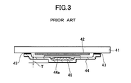
- Fig. 3 illustrates an example of such conventional organic EL display panel comprising a transparent glass substrate on which a sealing member is bonded. As shown in the drawing, an
organic layer 42 is formed on aglass substrate 41, and asealing member 44 is bonded by means of anadhesive layer 43 onto theglass substrate 41 so as to cover theorganic layer 42. The sealingmember 44 is provided with apocket 44a to hold adrying agent 45. - The
drying agent 45 is provided for absorbing and removing initial moisture existing inside the sealingmember 44 after the sealingmember 44 has been bonded to the glass substrate, as well as any other moistures dissipated or entered therein with the passing of time. This is because the organic layer, which is especially susceptible to heat attach, makes it impossible to perform heat treatment for completely removing moisture prior to the bonding process. As a result, the above moistures cannot be completely eliminated. For this reason, provision of thedrying agent 45 within the sealingmember 44 is indispensable to a display panel using current organic EL materials. Some exemplary substances which can be used as thedrying agent 45 are CaO, BaO, or the like which can chemically absorb moisture, or silica gel (or the like) which can physically absorb moisture. - According to the aforementioned prior art, the sealing member needs a thickness T in order to provide a pocket for installing the drying agent, and therefore there is a problem that the thickness of the entire organic EL display panel has to be increased. On the other hand, since an organic EL display panel is intended to be used as a display of a portable information terminal such as a portable telephone (also PDA and the like), a display panel with a reduced thickness is particularly highly required. Accordingly, it is necessary to minimize the size of a drying agent.
- Usually, a drying agent is required to act to absorb initial moisture existing inside the sealing member immediately after the bonding process, and to absorb moisture dissipated during the driving of the organic EL display panel or the moisture entering from outside during use. Accordingly, if the drying agent is too small in size, its moisture absorbing capability will be quickly used up in absorbing the initial moisture, and its action of absorbing the subsequent moisture produced thereafter will further decrease, leading to a problem of significantly shortening the usable life span of the organic EL display panel.
- The present invention has been accomplished in order to solve the aforementioned problems existing in the above-discussed prior art, and it is an object of the invention to provide an improved organic EL display panel having an elongated life span but a reduced thickness, as well as a method of manufacturing the organic EL display panel.
- To attain the above object, an organic EL display panel according to the present invention has the following features.
- According to a first aspect of the invention, there is provided an organic electroluminescent display panel including a transparent substrate, an organic layer formed on the transparent substrate, an adhesive layer formed around the organic layer, and a sealing member bonded to the transparent substrate by means of the adhesive layer for covering the organic layer, characterized in that: a photopolymerization initiator-containing resin capable of absorbing moisture by a photopolymerization reaction, is placed inside said sealing member, and has been radiated with a light and thus polymerized.
- According to a second aspect of the invention, based on the first aspect thereof, the adhesive layer comprises an ultraviolet-setting adhesive agent, and said photopolymerization initiator-containing resin is formed into a layer located along the adhesive layer.
- According to a third aspect of the invention, based on the first or second aspect thereof, the panel further comprises a drying agent placed inside the sealing member and capable of chemically or physically absorbing a moisture enclosed therein.
- According to a fourth aspect of the invention, there is provided a method of manufacturing an organic EL display panel, including the steps of: forming an organic layer on a transparent substrate; forming a light-setting resin layer serving as an adhesive around the organic layer by coating or printing; and bonding a sealing member for covering said organic layer to the transparent substrate by means of said adhesive layer. This method further comprises the steps of: forming a photopolymerization initiator-containing resin layer capable of absorbing moisture by a photopolymerization reaction, said resin layer being located along inner edges of said adhesive layer inside said sealing member and formed by coating or printing; and irradiating said adhesive resin layer and said photopolymerization initiator-containing resin layer with a light to simultaneously effect the curing of the adhesive resin layer and the photopolymerization of the photopolymerization initiator-containing resin layer.
- According to a fifth aspect, based on the manufacturing method of the fourth aspect, the sealing member is formed by a transparent material and said photopolymerization initiator-containing resin layer is formed on the inner surface of the sealing member. The method further comprising the step of attaching a drying agent to the inner surface of said sealing member at a position surrounded by said photoplymerization initiator-containing resin layer for chemically or physically absorbing moisture enclosed therein, followed by irradiating with an ultraviolet light through said sealing member.
- The present invention having the above feature has the following advantages.
- According to the first aspect of the invention, the photopolymerization initiator-containing resin layer capable of absorbing moisture by a photopolymerization reaction is placed inside the sealing member of the organic EL display panel. Therefore, immediately after the sealing member is bonded to the substrate, the photopolymerization initiator-containing resin layer undergoes photopolymerization to absorb the initial moisture existing inside the sealing member. In this way, the initial moisture can be promptly removed immediately after the bonding process. This prompt removal of the initial moisture makes it possible to minimize an influence of moisture produced at a later time in the organic EL display panel, resulting in an elongated life span for the organic EL display panel. In addition, the prompt removal of the initial moisture makes it possible to minimize the size of the drying agent, thereby reducing the thickness of the organic EL display panel.
- According to the second aspect of the invention, by forming the photopolymerization initiator-containing resin layer along the adhesive layer, the light radiation can be efficiently applied to both the adhesive layer and the photopolymerization initiator-containing resin layer.
- According to the third aspect of the invention, the photopolymerization initiator-containing resin layer initiates photopolymerization to absorb the initial moisture to thereby effectively remove it immediately after completion of the bonding process. Accordingly, the drying agent placed inside the sealing member is required to remove only the moisture entering thereafter, making it possible to minimize the size of the drying agent. Thus, it becomes possible for an organic EL display panel having a reduced thickness to provide an adequate life span.
- According to the fourth aspect of the invention, which is a method of manufacturing the organic EL display panel having the aforementioned features, the photopolymerization initiator-containing resin layer capable of absorbing moisture by the photopolymerization reaction is formed along the inner edges of the adhesive layer inside the sealing member by coating or printing, and the adhesive layer as well as the photopolymerization initiator-containing resin layer are irradiated with a light at one time. In this way, the initial moisture can be absorbed through the aforementioned photopolymerization when the adhesive is cured, rendering it possible to omit an extra step of irradiation with light for absorbing the initial moisture.
- According to the fifth aspect of the invention, the sealing member is formed by a transparent material and said photopolymerization initiator-containing resin layer is formed on the inner surface of the sealing member. The method further comprising the step of attaching a drying agent to the inner surface of said sealing member at a position surrounded by said photoplymerization initiator-containing resin layer for chemically or physically absorbing moisture enclosed therein, followed by irradiating with an ultraviolet light through said sealing member. Therefore, the curing of the adhesive resin layer and the photopolymerization of the photopolymerization initiator-containing resin layer can be effected during only one operation of the ultraviolet radiation. In addition, the drying agent functions as a mask, so that the light radiation does not cause deterioration of the organic layer even if an extra mask is not used. Further, providing the photopolymerization initiator-containing resin layer on the sealing member eliminates a dead space on the transparent substrate, and therefore an effective display area is ensured.
- These and other objects and features of the present invention will become more apparent from the following detailed description with reference to the accompanying drawings.
-
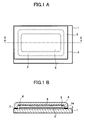
- Figs. 1A and 1B are a plan view and a sectional view illustrating an organic EL display panel according to a preferred embodiment of the present invention.
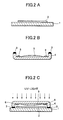
- Figs. 2A to 2C are sectional views explaining a method of manufacturing an organic EL display panel according to the embodiment of the present invention.
- Fig. 3 is a sectional view illustrating a conventional organic EL display panel.
-
- A preferred embodiment according to the present invention will be described hereinafter with reference to the accompanying drawings. Fig. 1A is an explanatory plan view of an organic EL display panel according to the preferred embodiment of the present invention, and Fig. 1B is a sectional view taken along the X-X line in Fig. 1A. In Figs. 1A and 1B, an
organic layer 2 is placed on aglass substrate 1. Theorganic layer 2 is formed by laminating: anodes (not shown) constituted by transparent electrodes of ITO or the like and formed on theglass substrate 1; a hole injection layer of copper phthalocyanines; a hole transporting layer of TDP or the like; a light-emitting layer or electron transporting layer of Alq3 or the like; an electron injection layer of LiO2; and cathodes (not shown) of Al or the like. - The
glass substrate 1 is bonded through anadhesive layer 3 with a glass-made sealingmember 4. Theadhesive layer 3 is formed by an ultraviolet setting resin such as an epoxy resin and located around theorganic layer 2. The sealingmember 4 has aninner face 4a on which adrying agent 5 is adhered. Thedrying agent 5 may either be a substance such as CaO, BaO or the like that chemically absorbs moisture, or silica gel or the like that physically absorbs moisture. - In the present embodiment, an initial
moisture absorbing layer 6 is formed along the inner sides of theadhesive layer 3 on theinner surface 4a of the sealingmember 4. The initialmoisture absorbing layer 6 comprises a photopolymerization initiator-containing resin capable of absorbing moisture by virtue of a photopolymerization reaction. For example, it is allowed to use an epoxy resin and a radical or a cationic photopolymerization initiator. Examples of a radical photopolymerization initiator include: diethoxy acetophenone; benzophenone; benzyl; benzoin isobutyl ether; benzyl dimethyl ketal; 1-hydroxycyclohexyl phenyl ketone; diethylthioxantone; 2-ethylanthraquinones; 2-hydroxy-2-methyl-1-phenylpropane-1-one; 1-(4-isopropylphenyl)-2-hydroxy-2-methylpropane-1-one; 2-methyl-[4-(methylthio)phenyl]-2-morpholino-1-propane; and the like. Examples of a substance used as a cationic photopolymerization initiator include aromatic diazonium salts, triallyl sulfonium salts, diallyl iodonium salts, triallyl selenium salts (all of which are salts of Lewis acid), a metallocene compound and the like. - Next, a description will be given to explain a method of manufacturing an organic EL display panel according to a preferred embodiment of the invention, with reference to Figs. 2A to 2C. Fig. 2A illustrates a state of the
organic layer 2 formed on theglass substrate 1. For forming theorganic layer 2, transparent electrodes of ITO or the like are formed as anodes on theglass substrate 1. Then, a hole injection layer, a hole transporting layer, a light-emitting layer, an electron transporting layer, an electron injection layer and the like are laminated successively on the transparent electrodes by vacuum deposition. Afterwards, electrodes of Al or the like serving as cathodes are deposited onto the resulting laminated layers. - Fig. 2B illustrates a state of the sealing
member 4 on which theadhesive layer 3, thedrying agent 5 and the initialmoisture absorbing layer 6 are formed. Theadhesive layer 3 is formed on the bonding face of the sealingmember 4 by coating (using a dispenser or the like), or by printing such as screen printing. Thedrying agent 5 is mixed into a resin, or solidified and has one face thereof coated with an adhesive, so as to be bonded as a thin-film to theinner face 4a of the sealingmember 4. The initialmoisture absorbing layer 6 is a mixture of the aforementioned resin and photopolymerization initiator, applied or printed on theinner face 4a of the sealingmember 4. Specifically, thelayer 6 is formed along the inner sides of theadhesive layer 3 so as to surround thedrying agent 5. - As shown in Fig. 2C, the resulting sealing
member 4 is then mounted on theglass substrate 1 so as to cover theorganic layer 3. Then, ultraviolet radiation is applied through the sealingmember 4 as indicated by the arrows in Fig. 2C in order to cure theadhesive layer 3 and cause the initialmoisture absorbing layer 6 to start photopolymerization so as to absorb initial moisture existing immediately after the bonding process. - With this method, the initial
moisture absorbing layer 6 produces an effect immediately after the sealingmember 4 is bonded around theorganic layer 2, so as to effectively remove the initial moisture existing inside the sealingmember 4. By removing the initial moisture, it is possible to reduce the moisture dissipated into a space inside the sealingmember 4 at a later time (when the organic EL display panel has been driven and the interior of the panel enclosed by the sealingmember 4 has been in an elevated temperature environment), thereby allowing thedrying agent 5 to be set at a low level of an absorbing activity. In this way, an amount of dryingagent 5 is allowed to be reduced, so that only a thin-thickness drying agent 5 is needed for ensuring an adequate life span for the display panel. Further, since a thin-thickness drying agent 5 is enough for ensuring an adequate life span for a display panel, a need for providing a pocket as in the prior art can be eliminated, thereby resulting in a decrease in the thickness of the display panel. - Further, in the present embodiment, the sealing
member 4 is made of glass, the initialmoisture absorbing layer 6 is provided along the inner sides of theadhesive layer 3 and thedrying agent 5 is adhered to the sealingmember 4 at a position surrounded by the absorbinglayer 6. With this arrangement, both the curing of theadhesive layer 3 and the photopolymerization of the initialmoisture absorbing layer 6 may be simultaneously effected by applying an ultraviolet radiation from above the sealingmember 4. And also, since thedrying agent 5 functions as a mask, theorganic layer 2 is prevented from deterioration (which will possibly be caused due to the ultraviolet radiation), thus making it possible to dispense with an extra mask. Further, providing the initialmoisture absorbing layer 6 on the sealingmember 4 eliminates a dead space on theglass substrate 1, thereby effectively ensuring a desired display area. - Using a glass to make the sealing
member 4 significantly reduces the weight of the sealing member as compared with a conventional metal-made sealing member. - According to the above-discussed embodiment, the
adhesive layer 3 and initialmoisture absorbing layer 6 are placed on the sealingmember 4. However, if either or both of thelayers glass substrate 1, it is still possible to increase the life span and reduce the thickness of a display panel, as described above. - The aforementioned embodiment provides the
drying agent 5, but if the initialmoisture absorbing layer 6 can completely remove the initial moisture, and if the subsequent entry of moisture from outside is avoidable by enhancing the sealing effect, a similar long life span of the panel can be ensured without providing thedrying agent 5. In this case, the sealingmember 4 can be further reduced in its thickness, resulting in a display panel compact in size. - The present invention is formed as described above, in which an initial moisture absorbing layer (constituted by a photopolymerization initiator-containing resin which absorbs moisture through a photopolymerization reaction) is placed inside a sealing member and is allowed to produce its effect after completion of the bonding process. Therefore, a longer life span of an organic EL display panel is achieved because of an effective and immediate removal of initial moisture existing inside the sealing member. Further, reduction in the thickness of the panel is achieved by minimizing the size of a drying agent.
- The terms and description used herein are set forth by way of illustration only and are not meant as limitations. Those skilled in the art will recognize that numerous variations are possible within the spirit and scope of the invention as defined in the following claims.
Claims (5)
- An organic electroluminescent display panel including a transparent substrate (1), an organic layer (2) formed on the transparent substrate (1), an adhesive layer (3) formed around the organic layer (2), and a sealing member (4)bonded to the transparent substrate (1) by means of the adhesive layer (3) for covering the organic layer (2), characterized in that:a photopolymerization initiator-containing resin (6) capable of absorbing moisture by a photopolymerization reaction, is placed inside said sealing member (4), and has been radiated with a light and thus polymerized.
- An organic electroluminescent display panel according to claim 1, wherein said adhesive layer (3) comprises an ultraviolet-setting adhesive agent, and said photopolymerization initiator-containing resin (6) is formed into a layer located along the adhesive layer (3).
- An organic electroluminescent display panel according to claim 1 or claim 2, further comprising a drying agent (5) placed inside the sealing member (4) and capable of chemically or physically absorbing a moisture enclosed therein.
- A method of manufacturing an organic electroluminescent display panel including the steps of: forming an organic layer (2) on a transparent substrate (1) ; forming a light-setting resin layer (3) serving as an adhesive around the organic layer (2) by coating or printing; and bonding a sealing member (4) for covering said organic layer (2) to the transparent substrate (1) by means of said adhesive layer (3), said method further comprising the steps of:forming a photopolymerization initiator-containing resin layer (6) capable of absorbing moisture by a photopolymerization reaction, said resin layer (6) being located along inner edges of said adhesive layer (3) inside said sealing member (4) and formed by coating or printing; andirradiating said adhesive resin layer (3) and said photopolymerization initiator-containing resin layer (6) with a light to simultaneously effect the curing of the adhesive resin layer (3) and the photopolymerization of the photopolymerization initiator-containing resin layer (6).
- A method of manufacturing an organic electroluminescent display panel according to claim 4,
wherein said sealing member (4) is formed by a transparent material and said photopolymerization initiator-containing resin layer (6) is formed on the inner surface of the sealing member (4),
said method further comprising the step of attaching a drying agent (5) to the inner surface of said sealing member (4) at a position surrounded by said photoplymerization initiator-containing resin layer (6) for chemically or physically absorbing moisture enclosed therein, followed by irradiating with an ultraviolet light through said sealing member (4).
Applications Claiming Priority (2)
| Application Number | Priority Date | Filing Date | Title |
|---|---|---|---|
| JP2001252505 | 2001-08-23 | ||
| JP2001252505 | 2001-08-23 |
Publications (1)
| Publication Number | Publication Date |
|---|---|
| EP1286566A1 true EP1286566A1 (en) | 2003-02-26 |
Family
ID=19080967
Family Applications (1)
| Application Number | Title | Priority Date | Filing Date |
|---|---|---|---|
| EP02018373A Withdrawn EP1286566A1 (en) | 2001-08-23 | 2002-08-14 | Organic electroluminescent display panel |
Country Status (3)
| Country | Link |
|---|---|
| US (1) | US6808828B2 (en) |
| EP (1) | EP1286566A1 (en) |
| KR (1) | KR20030017350A (en) |
Families Citing this family (27)
| Publication number | Priority date | Publication date | Assignee | Title |
|---|---|---|---|---|
| JP4090253B2 (en) * | 2002-03-08 | 2008-05-28 | 三洋電機株式会社 | Display device |
| TW584822B (en) * | 2002-03-28 | 2004-04-21 | Sanyo Electric Co | Organic electroluminescence panel |
| JP4050972B2 (en) * | 2002-10-16 | 2008-02-20 | 株式会社 日立ディスプレイズ | Display device |
| US20040189195A1 (en) * | 2003-03-24 | 2004-09-30 | Osram Opto Semiconductors Gmbh | Devices including, methods using, and compositions of reflowable getters |
| JP2004348971A (en) * | 2003-03-27 | 2004-12-09 | Tohoku Pioneer Corp | Organic EL display panel and manufacturing method thereof |
| KR100544128B1 (en) * | 2003-08-28 | 2006-01-23 | 삼성에스디아이 주식회사 | Organic EL display device having a porous material layer |
| JP2005340020A (en) * | 2004-05-27 | 2005-12-08 | Hitachi Displays Ltd | Organic electroluminescent display device and manufacturing method of the same |
| US20060001041A1 (en) * | 2004-07-01 | 2006-01-05 | Lightronik Technology Inc. | Organic light emitting device |
| JP2007287669A (en) * | 2006-03-23 | 2007-11-01 | Canon Inc | Organic light emitting device and method for manufacturing organic light emitting device |
| KR100747325B1 (en) * | 2006-05-01 | 2007-08-07 | 엘지전자 주식회사 | Electroluminescent element |
| KR100883075B1 (en) * | 2007-03-02 | 2009-02-10 | 엘지전자 주식회사 | Electroluminescent element |
| US20090006198A1 (en) * | 2007-06-29 | 2009-01-01 | David George Walsh | Product displays for retail stores |
| TWI443166B (en) | 2010-11-23 | 2014-07-01 | Lg Chemical Ltd | Adhesive composition |
| KR101353434B1 (en) | 2011-10-17 | 2014-01-21 | 주식회사 엘지화학 | Substrate for organic electronic device |
| CN103930503B (en) | 2011-11-14 | 2017-12-12 | Lg化学株式会社 | Bonding film |
| WO2013073847A1 (en) | 2011-11-14 | 2013-05-23 | 주식회사 엘지화학 | Adhesive film |
| KR20130108027A (en) | 2012-03-23 | 2013-10-02 | 주식회사 엘지화학 | Method for preparing substrate for organic electronic device |
| WO2015047036A1 (en) | 2013-09-30 | 2015-04-02 | 주식회사 엘지화학 | Substrate for organic electronic devices and production method therefor |
| JP6453871B2 (en) | 2013-09-30 | 2019-01-16 | エルジー ディスプレイ カンパニー リミテッド | Method for manufacturing organic electronic device |
| TWI581969B (en) | 2013-09-30 | 2017-05-11 | 樂金顯示科技股份有限公司 | Substrate for organic electronic devices |
| TWI593153B (en) | 2013-09-30 | 2017-07-21 | 樂金顯示科技股份有限公司 | Organic electronic device and its application |
| US9741951B2 (en) | 2013-09-30 | 2017-08-22 | Lg Chem, Ltd. | Substrate for organic electronic device and method for manufacturing same |
| KR101668907B1 (en) | 2013-11-21 | 2016-10-24 | 주식회사 엘지화학 | Gettering agent and moisture absorbent film using the same |
| US20150352521A1 (en) | 2013-11-21 | 2015-12-10 | Lg Chem, Ltd. | GETTERING AGENT, ABSORPTIVE FILM COMPRISING THE SAME AND ORGANIC ELECTRONIC DEVICE (As Amended) |
| KR101660692B1 (en) | 2013-12-27 | 2016-09-28 | 엘지디스플레이 주식회사 | Substrate for organic electronic device |
| KR102028142B1 (en) | 2014-12-31 | 2019-10-02 | 엘지디스플레이 주식회사 | Substrate for organic electronic device |
| KR101979780B1 (en) | 2015-09-11 | 2019-05-17 | 주식회사 엘지화학 | Moisture Absorbent Filler and Preparation Method for Manufacturing The Same |
Citations (4)
| Publication number | Priority date | Publication date | Assignee | Title |
|---|---|---|---|---|
| US4357557A (en) * | 1979-03-16 | 1982-11-02 | Sharp Kabushiki Kaisha | Glass sealed thin-film electroluminescent display panel free of moisture and the fabrication method thereof |
| EP0545558A1 (en) * | 1991-11-28 | 1993-06-09 | Nippon Seiki K.K. | Display panel with electroluminescent illumination |
| JP2001139933A (en) * | 1999-08-12 | 2001-05-22 | Mitsui Chemicals Inc | Photocurable resin composition for sealing agent and sealing method |
| EP1115267A2 (en) * | 1999-12-28 | 2001-07-11 | Nec Corporation | Organic electro-luminescent display panel and method for manufacturing same |
Family Cites Families (8)
| Publication number | Priority date | Publication date | Assignee | Title |
|---|---|---|---|---|
| US6081071A (en) * | 1998-05-18 | 2000-06-27 | Motorola, Inc. | Electroluminescent apparatus and methods of manufacturing and encapsulating |
| JP2000195660A (en) * | 1998-12-25 | 2000-07-14 | Tdk Corp | Organic EL device |
| US6226890B1 (en) * | 2000-04-07 | 2001-05-08 | Eastman Kodak Company | Desiccation of moisture-sensitive electronic devices |
| US6819042B2 (en) * | 2000-05-17 | 2004-11-16 | Dynic Corporation | Organic EL device and method for its manufacture |
| TWI222838B (en) * | 2001-04-10 | 2004-10-21 | Chi Mei Optoelectronics Corp | Packaging method of organic electroluminescence light-emitting display device |
| CN100380703C (en) * | 2001-05-18 | 2008-04-09 | 皇家菲利浦电子有限公司 | Hygroscopic board |
| TW515062B (en) * | 2001-12-28 | 2002-12-21 | Delta Optoelectronics Inc | Package structure with multiple glue layers |
| US6936131B2 (en) * | 2002-01-31 | 2005-08-30 | 3M Innovative Properties Company | Encapsulation of organic electronic devices using adsorbent loaded adhesives |
-
2002
- 2002-08-13 US US10/216,892 patent/US6808828B2/en not_active Expired - Fee Related
- 2002-08-14 EP EP02018373A patent/EP1286566A1/en not_active Withdrawn
- 2002-08-20 KR KR1020020049164A patent/KR20030017350A/en not_active Withdrawn
Patent Citations (4)
| Publication number | Priority date | Publication date | Assignee | Title |
|---|---|---|---|---|
| US4357557A (en) * | 1979-03-16 | 1982-11-02 | Sharp Kabushiki Kaisha | Glass sealed thin-film electroluminescent display panel free of moisture and the fabrication method thereof |
| EP0545558A1 (en) * | 1991-11-28 | 1993-06-09 | Nippon Seiki K.K. | Display panel with electroluminescent illumination |
| JP2001139933A (en) * | 1999-08-12 | 2001-05-22 | Mitsui Chemicals Inc | Photocurable resin composition for sealing agent and sealing method |
| EP1115267A2 (en) * | 1999-12-28 | 2001-07-11 | Nec Corporation | Organic electro-luminescent display panel and method for manufacturing same |
Non-Patent Citations (1)
| Title |
|---|
| DATABASE WPI Section Ch Week 200134, Derwent World Patents Index; Class A89, AN 2001-257527, XP002222633 * |
Also Published As
| Publication number | Publication date |
|---|---|
| KR20030017350A (en) | 2003-03-03 |
| US20030039859A1 (en) | 2003-02-27 |
| US6808828B2 (en) | 2004-10-26 |
Similar Documents
| Publication | Publication Date | Title |
|---|---|---|
| US6808828B2 (en) | Organic electroluminescent display panel | |
| TWI245251B (en) | Display device | |
| TWI233316B (en) | Organic electroluminescent device and method of manufacturing the same | |
| JP4479381B2 (en) | Electro-optical device, method of manufacturing electro-optical device, and electronic apparatus | |
| KR101930129B1 (en) | Organic el panel and method for manufacturing the same | |
| US8519621B2 (en) | Organic light emitting display and method for manufacturing the same | |
| KR100722941B1 (en) | Light-emitting device, method of manufacturing the same, and electronic equipment | |
| JP2001035659A (en) | Organic electroluminescent device and method of manufacturing the same | |
| TWI277919B (en) | Light emitting device, method of manufacturing light emitting device, and electronic apparatus | |
| US6717052B2 (en) | Housing structure with multiple sealing layers | |
| KR100711882B1 (en) | Organic electroluminescent display and manufacturing method thereof | |
| CN101728338B (en) | Light emitting display and method of manufacturing the same | |
| KR20010062831A (en) | Organic electro-luminescent display panel and method for manufacturing same | |
| TWI398975B (en) | Method for manufacturing organic electroluminescent display | |
| JP4539368B2 (en) | Manufacturing method of display device | |
| GB2421117A (en) | Light emitting display panel | |
| JP2006024421A (en) | Electro-optical device, method of manufacturing electro-optical device, and electronic apparatus | |
| JP4605499B2 (en) | Organic EL display sealing structure | |
| JP3932660B2 (en) | Manufacturing method of EL display device | |
| JP2003243161A (en) | Manufacturing method and manufacturing apparatus for electro-optical device, electro-optical device, and electronic equipment | |
| JP2000311782A (en) | Organic EL display and manufacturing method thereof | |
| JP2003297555A (en) | Manufacturing method of organic EL display and substrate for organic EL display | |
| JP3928944B2 (en) | Organic EL display panel | |
| JP2000223261A (en) | Color electroluminescent display device and method of manufacturing the same | |
| KR101007722B1 (en) | Flat Panel Display and Manufacturing Method |
Legal Events
| Date | Code | Title | Description |
|---|---|---|---|
| PUAI | Public reference made under article 153(3) epc to a published international application that has entered the european phase |
Free format text: ORIGINAL CODE: 0009012 |
|
| AK | Designated contracting states |
Kind code of ref document: A1 Designated state(s): AT BE BG CH CY CZ DE DK EE ES FI FR GB GR IE IT LI LU MC NL PT SE SK TR Designated state(s): AT BE BG CH CY CZ DE DK EE ES FI FR GB GR IE IT LI LU MC NL PT SE SK TR |
|
| AX | Request for extension of the european patent |
Extension state: AL LT LV MK RO SI |
|
| 17P | Request for examination filed |
Effective date: 20030627 |
|
| AKX | Designation fees paid |
Designated state(s): DE FR GB |
|
| 17Q | First examination report despatched |
Effective date: 20070809 |
|
| STAA | Information on the status of an ep patent application or granted ep patent |
Free format text: STATUS: THE APPLICATION HAS BEEN WITHDRAWN |
|
| 18W | Application withdrawn |
Effective date: 20070907 |