EP1286399B1 - LDMOS field-effect transistors - Google Patents
LDMOS field-effect transistors Download PDFInfo
- Publication number
- EP1286399B1 EP1286399B1 EP02255829A EP02255829A EP1286399B1 EP 1286399 B1 EP1286399 B1 EP 1286399B1 EP 02255829 A EP02255829 A EP 02255829A EP 02255829 A EP02255829 A EP 02255829A EP 1286399 B1 EP1286399 B1 EP 1286399B1
- Authority
- EP
- European Patent Office
- Prior art keywords
- region
- distance
- transistor
- conductivity type
- curved
- Prior art date
- Legal status (The legal status is an assumption and is not a legal conclusion. Google has not performed a legal analysis and makes no representation as to the accuracy of the status listed.)
- Expired - Lifetime
Links
Images



Classifications
-
- H—ELECTRICITY
- H10—SEMICONDUCTOR DEVICES; ELECTRIC SOLID-STATE DEVICES NOT OTHERWISE PROVIDED FOR
- H10D—INORGANIC ELECTRIC SEMICONDUCTOR DEVICES
- H10D30/00—Field-effect transistors [FET]
- H10D30/60—Insulated-gate field-effect transistors [IGFET]
- H10D30/64—Double-diffused metal-oxide semiconductor [DMOS] FETs
- H10D30/65—Lateral DMOS [LDMOS] FETs
-
- H—ELECTRICITY
- H10—SEMICONDUCTOR DEVICES; ELECTRIC SOLID-STATE DEVICES NOT OTHERWISE PROVIDED FOR
- H10D—INORGANIC ELECTRIC SEMICONDUCTOR DEVICES
- H10D62/00—Semiconductor bodies, or regions thereof, of devices having potential barriers
- H10D62/10—Shapes, relative sizes or dispositions of the regions of the semiconductor bodies; Shapes of the semiconductor bodies
- H10D62/124—Shapes, relative sizes or dispositions of the regions of semiconductor bodies or of junctions between the regions
- H10D62/126—Top-view geometrical layouts of the regions or the junctions
-
- H—ELECTRICITY
- H10—SEMICONDUCTOR DEVICES; ELECTRIC SOLID-STATE DEVICES NOT OTHERWISE PROVIDED FOR
- H10D—INORGANIC ELECTRIC SEMICONDUCTOR DEVICES
- H10D62/00—Semiconductor bodies, or regions thereof, of devices having potential barriers
- H10D62/10—Shapes, relative sizes or dispositions of the regions of the semiconductor bodies; Shapes of the semiconductor bodies
- H10D62/124—Shapes, relative sizes or dispositions of the regions of semiconductor bodies or of junctions between the regions
- H10D62/126—Top-view geometrical layouts of the regions or the junctions
- H10D62/127—Top-view geometrical layouts of the regions or the junctions of cellular field-effect devices, e.g. multicellular DMOS transistors or IGBTs
-
- H—ELECTRICITY
- H10—SEMICONDUCTOR DEVICES; ELECTRIC SOLID-STATE DEVICES NOT OTHERWISE PROVIDED FOR
- H10D—INORGANIC ELECTRIC SEMICONDUCTOR DEVICES
- H10D64/00—Electrodes of devices having potential barriers
- H10D64/20—Electrodes characterised by their shapes, relative sizes or dispositions
- H10D64/27—Electrodes not carrying the current to be rectified, amplified, oscillated or switched, e.g. gates
- H10D64/311—Gate electrodes for field-effect devices
- H10D64/411—Gate electrodes for field-effect devices for FETs
- H10D64/511—Gate electrodes for field-effect devices for FETs for IGFETs
- H10D64/517—Gate electrodes for field-effect devices for FETs for IGFETs characterised by the conducting layers
- H10D64/519—Gate electrodes for field-effect devices for FETs for IGFETs characterised by the conducting layers characterised by their top-view geometrical layouts
-
- H—ELECTRICITY
- H10—SEMICONDUCTOR DEVICES; ELECTRIC SOLID-STATE DEVICES NOT OTHERWISE PROVIDED FOR
- H10D—INORGANIC ELECTRIC SEMICONDUCTOR DEVICES
- H10D62/00—Semiconductor bodies, or regions thereof, of devices having potential barriers
- H10D62/10—Shapes, relative sizes or dispositions of the regions of the semiconductor bodies; Shapes of the semiconductor bodies
- H10D62/13—Semiconductor regions connected to electrodes carrying current to be rectified, amplified or switched, e.g. source or drain regions
- H10D62/149—Source or drain regions of field-effect devices
- H10D62/151—Source or drain regions of field-effect devices of IGFETs
- H10D62/156—Drain regions of DMOS transistors
- H10D62/157—Impurity concentrations or distributions
-
- H—ELECTRICITY
- H10—SEMICONDUCTOR DEVICES; ELECTRIC SOLID-STATE DEVICES NOT OTHERWISE PROVIDED FOR
- H10D—INORGANIC ELECTRIC SEMICONDUCTOR DEVICES
- H10D62/00—Semiconductor bodies, or regions thereof, of devices having potential barriers
- H10D62/10—Shapes, relative sizes or dispositions of the regions of the semiconductor bodies; Shapes of the semiconductor bodies
- H10D62/17—Semiconductor regions connected to electrodes not carrying current to be rectified, amplified or switched, e.g. channel regions
- H10D62/393—Body regions of DMOS transistors or IGBTs
-
- H—ELECTRICITY
- H10—SEMICONDUCTOR DEVICES; ELECTRIC SOLID-STATE DEVICES NOT OTHERWISE PROVIDED FOR
- H10D—INORGANIC ELECTRIC SEMICONDUCTOR DEVICES
- H10D64/00—Electrodes of devices having potential barriers
- H10D64/20—Electrodes characterised by their shapes, relative sizes or dispositions
- H10D64/27—Electrodes not carrying the current to be rectified, amplified, oscillated or switched, e.g. gates
- H10D64/311—Gate electrodes for field-effect devices
- H10D64/411—Gate electrodes for field-effect devices for FETs
- H10D64/511—Gate electrodes for field-effect devices for FETs for IGFETs
- H10D64/514—Gate electrodes for field-effect devices for FETs for IGFETs characterised by the insulating layers
- H10D64/516—Gate electrodes for field-effect devices for FETs for IGFETs characterised by the insulating layers the thicknesses being non-uniform
Definitions
- the invention relates to lateral double-diffused metal-oxide-semiconductor (LDMOS) transistors and, in particular, to an LDMOS transistor with improved ruggedness at curved areas.
- LDMOS metal-oxide-semiconductor
- LDMOS Lateral double-diffused metal-oxide-semiconductor
- Device modelling typically involves only two-dimensional (2D) analysis of an LDMOS transistor (that is, the depth and the length of the transistor). Such 2D modelling neglects three-dimensional effects on the surface of the transistor.
- 2D modelling neglects three-dimensional effects on the surface of the transistor.
- the layout geometry of an LDMOS transistor can have an adverse impact on device characteristics, such as the breakdown voltage, of the transistor.
- the layout geometry of an LDMOS transistor includes curved regions such as when the transistor is shaped in a race-track or in loops, the LDMOS transistor can suffer from a low breakdown voltage at the curved regions due to electric field crowding effects.
- Electric field crowding effects describe the conditions where the surface electric field of an LDMOS transistor is higher at the curved regions of the transistor as compared to the parallel regions due to electric field crowding at the curved regions.
- Figure 2 illustrates a conventional race-track layout geometry of a LDMOS transistor. Because of electric field crowding effects, the breakdown voltages of the curved end regions (regions 20 and 22) are lower than the breakdown voltages of the parallel or rectilinear regions. Thus, the breakdown voltage of the LDMOS transistor is limited by the breakdown voltage of the curved regions.
- a method for reducing the electric field crowding at the curved regions of an LDMOS transistor has been proposed where the buried layer in the LDMOS transistor is extended towards the drain of the transistor. (See, M. Amato, "Reduced Electric Field Crowding at the Fingertips of Lateral DMOS Transistors," Proceedings of the Electrochemical Society, pp. 161-162, 1987 ).
- JP-A-10050985 discloses an elongated source region where the two larger sides are parallel and the two shorter sides are semicircular and have diameters equal to a distance between parallel sides.
- a heavily doped p-type region is provided as a well contact, and heavily doped n-type drain regions are located opposite the parallel sides of the source region, but not facing the curved ends of the source region.
- EP 1089345 discloses a semiconductor device which comprises an n-type well formed on a p-type substrate, and a drain region disposed in the n-type well.
- a p-type base surrounds the n-type well, and the p-type base and the drain have straight portions separated by an uniform interval.
- a corner part is formed at an end portion of the straight portions.
- the interval between the p-type base and the drain is larger than the interval between the straight portions, and the conductivity characteristics in the larger interval region are different from those of the n-type well along a predetermined width in order to relieve the concentration of electric fields at the corner part.
- a lateral DMOS transistor structure comprising:
- the drain region of the LDMOS transistor can be formed in an N-well formed in the N-epitaxial layer.
- the enhancement schemes optimize the breakdown voltage characteristics and ruggedness of the lateral DMOS transistor in both the rectilinear and curved regions.
- a lateral double-diffused metal-oxide-semiconductor (LDMOS) transistor where the breakdown voltage is optimized over the entire geometry of the transistor.
- the LDMOS transistor of the present invention obviates the electric field crowding effects by extending the drift regions at the curved regions of the transistor and the electric field in the drift region of the curved region is dispersed by extending the gate conductor overlap on the field oxide region between the gate conductor and the drain region. In this manner, the electric field at the curved regions of the LDMOS transistor can be made to be equal to or lower than that of the rectilinear regions.
- the breakdown voltage of the LDMOS transistor can be optimized for the entire geometry of the transistor instead of being limited by the curved regions where crowding of the electric field decreases the breakdown voltage that can be sustained.
- the LDMOS transistor of the present invention has usage in high voltage applications, such as those in the range of 60 to 1000 volts.
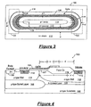
- FIG 3 is a top view of an LDMOS transistor formed in a race-track shaped geometry illustrating the various regions of the transistor according to one embodiment of the present invention.
- a cross-sectional view of the LDMOS transistor at the curved end of the transistor along the line A-A' is shown in Figure 4 .
- LDMOS transistor 100 is built on a p-type substrate 102 having a resistivity of approximately 7 ohm-cm.
- An N-epitaxial layer 104 of approximately 7.5 microns thick is then grown on the surface of substrate 102 using conventional techniques.
- the resistivity of epitaxial layer 104 can be approximately 3 ohm-cm.
- Transistor 100 may include an optional p-type buried layer 106 for shaping the electric field in the channel region and the drift region of the transistor.
- N-epitaxial layer 104 On the surface of N-epitaxial layer 104, an oxide layer 107 is formed to insulate a gate 108 from the substrate.
- the gate oxide layer is typically thermally grown and has a thickness of approximately 50 nm.
- Gate 108 is typically a polysilicon layer deposited and patterned using conventional techniques.
- Formed within N-epitaxial layer 104 also include an N+ source region 110, an N+ drain region 112, a p-type well region 114 which is used as the body region of the LDMOS transistor, and an N-type well region 105.
- N-type well region 105 is optional and in other embodiments, LDMOS transistor 100 can be formed directly in N-epitaxial layer 104, as will be discussed in more detail below.
- a p+ body contact region 116 is formed for making contact to p-type well region 114.
- LDMOS transistor 100 includes a field oxide region 118 extending from underneath the source side of gate 108 to drain region 112. Field oxide region 118 is included to reduce the Miller capacitance of the transistor and increase the breakdown voltage between gate 108 and drain region 112, as is understood by one skilled in the art. LDMOS transistor 100 thus formed includes a drift region extending from the edge of p-type well region 114 to drain region 112. In Figure 4 , the drift region is denoted by the distance d+d'.
- LDMOS transistor 100 When LDMOS transistor 100 is formed in a race-track shaped geometry as shown in Figure 3 or any other geometry including curved regions, the breakdown voltage characteristics and the ruggedness of the transistor are limited by the characteristics at the curved regions because of electric field crowding effects. This is often undesirable particularly because the curved region constitutes only a small portion of the entire width of the LDMOS transistor.
- enhancement schemes for improving the breakdown voltage characteristics and the ruggedness of the LDMOS transistor at the curved end regions are provided so that the overall performance of the transistor can be enhanced.
- the first enhancement scheme for improving the breakdown voltage characteristics and the ruggedness of LDMOS transistor 100 involves selectively extending the drift region of the LDMOS transistor.
- LDMOS transistor 100 is formed with a varied length drift region where the drift region at the curved ends (regions 120 and 122) of the race-track geometry is extended in order to reduce the effect of electric field crowding in these curved regions.
- the breakdown voltage characteristics of LDMOS transistor 100 can be made uniform across the entire width of the transistor and the breakdown voltage of transistor 100 is no longer limited by the curved regions inflicted with higher electric field due to electric field crowding.
- the drift region in the rectilinear regions of LDMOS transistor 100 has a length of d while the maximum drift region in the curved regions (regions 120 and 122) has a length of d+d', where d' is the extended length of the drift region in the curved regions.
- the length d is chosen to give the desired breakdown voltage of LDMOS transistor 100, and the length of d+d' is chosen to give the same desired breakdown voltage.
- the drift region of the transistor is the sum of the lengths g', h, h' and o, where g'+h+h' represents the length of field oxide region 118, h+h' represents the amount of gate 108 overlap of the field oxide region, and o represents the length from the edge of the p-type well region 114 to the edge of field oxide region 118.
- the drift region of transistor 100 is extended by extending field oxide region 118 to a length of g'+h+h', resulting in an additional field oxide length of d'.
- LDMOS transistor 100 can attain improved performance in breakdown voltage characteristics without severely compromising other device characteristics, such as a large increase in on-resistance. If the entire length of field oxide region 118 is extended to accommodate the curved regions, the on-resistance or other device characteristics of LDMOS transistor 100 can be severely compromised.
- the length of field oxide region 118 is extended by at least 50% at the widest point in the curved regions.
- the field oxide length extension is introduced gradually from the rectilinear regions to the curved end regions to provide a smooth interface, as illustrated in Figure 3 .
- the length of field oxide region 118 in the rectilinear regions of LDMOS transistor 100 can be 6 ⁇ m and the length of field oxide region 118 in the curved regions of the transistor can be 9 ⁇ m at the widest point.
- another enhancement scheme for improving the breakdown voltage characteristics and ruggedness of transistor 100 involves extending the gate conductor overlap of the field oxide region.
- gate 108 overlaps field oxide region 118 by a length of h, while in the curved end regions (regions 120 and 122), gate 108 overlaps field oxide region 118 by a length of h+h'.
- the cross-sectional view in Figure 4 shows gate 108 overlapping gate oxide region by h+h' in the curved end regions. Extending the gate-over-field-oxide overlap by h' has the effect of spreading out the electric field under gate 108 so that the intensity of the electric field near the gate oxide region is reduced.
- the gate-over-field-oxide overlap is increased by at least 100% at the widest point in the curved regions of the transistor.
- the gate conductor extension is introduced gradually from the rectilinear regions to the curved end regions to provide a smooth interface, as illustrated in Figure 3 .
- the length h of the gate over field oxide overlap in the rectilinear regions of LDMOS transistor 100 can be 3 ⁇ m and the length h+h' of the gate over field oxide overlap in the curved regions of the transistor can be 6 ⁇ m at the widest point.
- LDMOS transistor 100 incorporates both enhancement schemes of improving the breakdown voltage characteristics and ruggedness of the transistor described above. That is, LDMOS transistor 100 includes an extended drift region and an extended gate-over-field-oxide overlap in the curved regions. In other embodiments, it is of course possible to incorporate only the second scheme in an LDMOS transistor as long as the desired device characteristics can be obtained.
- FIG. 5 is a cross-sectional view of an LDMOS transistor 200 according to another embodiment of the present invention. Like elements in Figures 4 and 5 are given like reference numerals to simplify the discussion. As described above, N-well 105 of LDMOS transistor 100 is optional. Thus in the embodiment shown in Figure 5 , LDMOS transistor 200 is formed in N-type epitaxial layer 104 without an N-well. The enhancement schemes described above can be applied to LDMOS transistor 200 in the same manner as LDMOS transistor 100 for effectively improving the breakdown voltage characteristics and ruggedness of LDMOS transistor 200 while not severely compromising the on-resistance of the transistor.
- LDMOS transistor 100 in Figure 3 has been simplified for ease of discussion. Of course, in actual implementation, LDMOS transistor 100 may include other device structures not shown in Figure 3 .
- Figure 6 illustrates an LDMOS transistor according to another embodiment of the present invention.
- LDMOS transistor 300 of Figure 6 is shown including body, source and drain contacts disposed throughout the transistor.
- LDMOS transistor 300 includes an additional field oxide region 350 between source region 310 and body contact region 316. Field oxide region 350 is included when butted contact structure is not used in the fabrication process or to provide a higher source to body voltage. In other embodiments, when butted contacts can be formed in the fabrication process, body contact region 316 and source region 310 can be contiguous.
- Figures 3-6 illustrate embodiments of the present invention where the breakdown voltage/ruggedness enhancement schemes are applied to the conventional LDMOS transistor structure of Figure 1 .
- the breakdown voltage/ruggedness enhancement schemes of the present invention can be applied to a variety of LDMOS transistor structures.
- U.S. Patent No. 5,517,046 issued to Hsing et al. discloses improvements on the conventional LDMOS structure for enhancing the breakdown voltage while maintaining a low on-resistance.
- the breakdown voltage/ruggedness enhancement schemes of the present invention can be applied to an LDMOS transistor as described in the '046 patent where an enhanced drift region is included between the gate and the drain region.
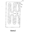
- FIG. 7 illustrates a portion of an LDMOS transistor 400 according to one embodiment of the present invention where the transistor assumes a serpentine shape.
- LDMOS transistor 400 includes extended gate-over-field-oxide overlaps at each curved regions of the serpentine-shaped layout.
- LDMOS transistor 400 includes both extended drift regions and extended gate-over-field-oxide overlaps at each curved regions of the serpentine-shaped layout.
- FIG. 8 is a top view of an LDMOS transistor 500 according to another embodiment of the present invention.
- Figure 8 illustrates the application of the schemes of the present invention to an LDMOS transistor in a trapped-drain configuration.
- gate conductor 508 encloses N+ drain region 512.
- the length of field oxide region 518 in the curved region is extended so that the drift region is increased by d' as compared to the length d of the drift region in the rectilinear region.
- the gate-over-field-oxide overlap in the curved region is extended by h' as compared to the length h of the overlap in the rectilinear region.
- the length of field oxide region 518 is extended by at least 40% at the widest point in the curved regions.
- the field oxide length extension is introduced gradually from the rectilinear regions to the curved end regions to provide a smooth interface, as illustrated in Figure 8 .
- the length d of field oxide region 518 in the rectilinear regions of LDMOS transistor 500 is 10 ⁇ m and the length d+d' of field oxide region 518 in the curved regions of the transistor is 14 ⁇ m at the widest point.
- the gate-over-field-oxide overlap is increased by at least 66% at the widest point in the curved regions of the transistor.
- the gate conductor extension is introduced gradually from the rectilinear regions to the curved end regions to provide a smooth interface, as illustrated in Figure 8 .
- the length h of the gate over field oxide overlap in the rectilinear regions of LDMOS transistor 500 is 6 ⁇ m and the length h+h' of the gate over field oxide overlap in the curved regions of the transistor 10 ⁇ m at the widest point.
- the present invention proposes using the trapped-source configuration because it provides additional advantages not possible with the trapped-drain configuration.
- the drain regions of the LDMOS transistor together with the p-type up-isolation and down-isolation regions can be used to form an electrostatic discharge (ESD) protection diode.
- ESD electrostatic discharge
- up-isolation and down-isolation regions are used for isolating the tubs (or p-wells and n-wells) in conventional BICMOS fabrication processes. When thus configured, the ESD immunity level of the LDMOS transistor can be dramatically improved.
- the breakdown voltage characteristics of the transistor are optimized such that the breakdown voltages at curved sections are made the same as or better than the breakdown voltage at the rectilinear sections.
- the breakdown voltage characteristics can be made uniform throughout the LDMOS transistor regardless of the layout geometry.
- the ESD immunity of the transistor is also improved.
- the thin gate oxide underneath the gate conductor can be protected from ESD events in both the rectilinear and curved sections.
- the schemes of the present invention allows breakdown voltages to be equalized without severely and negatively impacting the on-resistance or other devices characteristics of the transistor. The advantages achieved by the breakdown voltage/ruggedness enhancement schemes of the present invention have not been realized before.
Landscapes
- Insulated Gate Type Field-Effect Transistor (AREA)
Description
- The invention relates to lateral double-diffused metal-oxide-semiconductor (LDMOS) transistors and, in particular, to an LDMOS transistor with improved ruggedness at curved areas.
- Lateral double-diffused metal-oxide-semiconductor (LDMOS) transistors are commonly used in high-voltage applications because of their high breakdown voltage characteristics.
Figure 1 is a cross-sectional view of a conventional LDMOS transistor. It is well known that by increasing the length of the drift region, denoted by the distance "d", the breakdown voltage of the LDMOS transistor can be accordingly increased. - Device modelling typically involves only two-dimensional (2D) analysis of an LDMOS transistor (that is, the depth and the length of the transistor). Such 2D modelling neglects three-dimensional effects on the surface of the transistor. It is well known that the layout geometry of an LDMOS transistor can have an adverse impact on device characteristics, such as the breakdown voltage, of the transistor. Specifically, when the layout geometry of an LDMOS transistor includes curved regions such as when the transistor is shaped in a race-track or in loops, the LDMOS transistor can suffer from a low breakdown voltage at the curved regions due to electric field crowding effects. Electric field crowding effects describe the conditions where the surface electric field of an LDMOS transistor is higher at the curved regions of the transistor as compared to the parallel regions due to electric field crowding at the curved regions.
-
Figure 2 illustrates a conventional race-track layout geometry of a LDMOS transistor. Because of electric field crowding effects, the breakdown voltages of the curved end regions (regions 20 and 22) are lower than the breakdown voltages of the parallel or rectilinear regions. Thus, the breakdown voltage of the LDMOS transistor is limited by the breakdown voltage of the curved regions. A method for reducing the electric field crowding at the curved regions of an LDMOS transistor has been proposed where the buried layer in the LDMOS transistor is extended towards the drain of the transistor. (See, M. Amato, "Reduced Electric Field Crowding at the Fingertips of Lateral DMOS Transistors," Proceedings of the Electrochemical Society, pp. 161-162, 1987). While this method is effective in improving the breakdown voltage in the curved regions of an LDMOS transistor to match that of the parallel regions, the method also results in an overall increase in the on-resistance (Ron) of the LDMOS transistor. A large increase in on-resistance of a transistor is undesirable, especially for high-voltage applications. - Therefore, it is desirable to optimize the breakdown voltage characteristics of an LDMOS transistor over the entire layout geometry of the transistor without severely impacting other device characteristics of the transistor.
-
JP-A-10050985 -
EP 1089345 discloses a semiconductor device which comprises an n-type well formed on a p-type substrate, and a drain region disposed in the n-type well. A p-type base surrounds the n-type well, and the p-type base and the drain have straight portions separated by an uniform interval. A corner part is formed at an end portion of the straight portions. At the corner part of the drain, the interval between the p-type base and the drain is larger than the interval between the straight portions, and the conductivity characteristics in the larger interval region are different from those of the n-type well along a predetermined width in order to relieve the concentration of electric fields at the corner part. - According to an aspect of the present invention there is provided a lateral DMOS transistor structure comprising:
- a semiconductor material of a first conductivity type, said semiconductor material having a first dopant concentration and a top surface;
- a first region formed in said semiconductor material, said first region being of said first conductivity type and having a second dopant concentration to form a drain region of said DMOS transistor;
- a second region formed in said semiconductor material, said second region being of a second conductivity type and having a third dopant concentration to form a body region of said DMOS transistor, said second region having a first end underlying a conductive gate, any remaining portion of said semiconductor material underlying said conductive gate being in said first conductivity type;
- a third region formed in said semiconductor material, said third region being of said first conductivity type and having said second dopant concentration to form a source region of said DMOS transistor, said third region being located within said second region; and
- an oxide region comprising a gate oxide region and a field oxide region, said field oxide region formed on said top surface of said semiconductor material and having a portion extending into said top surface, said field oxide region having a first end thereof adjacent and in contact with said first region and wherein said gate oxide region has a smaller thickness than that of the field oxide region; and
- said conductive gate overlying and insulated from said top surface of said semiconducting material, said conductive gate having a geometric shape in the plane of the substrate including a rectilinear region and a curved region and formed such that it overlies a second end of said field oxide region;
- In other embodiments, the drain region of the LDMOS transistor can be formed in an N-well formed in the N-epitaxial layer.
- The enhancement schemes optimize the breakdown voltage characteristics and ruggedness of the lateral DMOS transistor in both the rectilinear and curved regions.
- The present invention is described further hereinafter by way of example only with reference to the accompanying drawings in which:
-
Fig. 1 is a cross-sectional view of a conventional LDMOS transistor. -
Fig. 2 illustrates a conventional race-track layout geometry of a LMDOS transistor. -
Fig. 3 is a top view of an LDMOS transistor formed in a race-track shaped geometry illustrating the various regions of the transistor according to one embodiment of the present invention. -
Figure 4 is a cross-sectional view of the LDMOS transistor ofFigure 3 at the curved end of the transistor along the line A-A'. -
Figure 5 is a cross-sectional view of an LDMOS transistor according to another embodiment of the present invention. -
Figure 6 illustrates an LDMOS transistor according to another embodiment of the present invention. -
Figure 7 illustrates a portion of an LDMOS transistor according to one embodiment of the present invention where the transistor assumes a serpentine shape. -
Figure 8 is a top view of an LDMOS transistor according to another embodiment of the present invention. - In the present disclosure, like objects which appear in more than one figure are provided with like reference numerals.
- In accordance with the present invention a lateral double-diffused metal-oxide-semiconductor (LDMOS) transistor is provided where the breakdown voltage is optimized over the entire geometry of the transistor. In one embodiment, the LDMOS transistor of the present invention obviates the electric field crowding effects by extending the drift regions at the curved regions of the transistor and the electric field in the drift region of the curved region is dispersed by extending the gate conductor overlap on the field oxide region between the gate conductor and the drain region. In this manner, the electric field at the curved regions of the LDMOS transistor can be made to be equal to or lower than that of the rectilinear regions. The breakdown voltage of the LDMOS transistor can be optimized for the entire geometry of the transistor instead of being limited by the curved regions where crowding of the electric field decreases the breakdown voltage that can be sustained. The LDMOS transistor of the present invention has usage in high voltage applications, such as those in the range of 60 to 1000 volts.
-
Figure 3 is a top view of an LDMOS transistor formed in a race-track shaped geometry illustrating the various regions of the transistor according to one embodiment of the present invention. A cross-sectional view of the LDMOS transistor at the curved end of the transistor along the line A-A' is shown inFigure 4 . In the present embodiment,LDMOS transistor 100 is built on a p-type substrate 102 having a resistivity of approximately 7 ohm-cm. An N-epitaxial layer 104 of approximately 7.5 microns thick is then grown on the surface ofsubstrate 102 using conventional techniques. The resistivity ofepitaxial layer 104 can be approximately 3 ohm-cm.Transistor 100 may include an optional p-type buriedlayer 106 for shaping the electric field in the channel region and the drift region of the transistor. - On the surface of N-
epitaxial layer 104, anoxide layer 107 is formed to insulate agate 108 from the substrate. The gate oxide layer is typically thermally grown and has a thickness of approximately 50 nm.Gate 108 is typically a polysilicon layer deposited and patterned using conventional techniques. Formed within N-epitaxial layer 104 also include anN+ source region 110, anN+ drain region 112, a p-type well region 114 which is used as the body region of the LDMOS transistor, and an N-type well region 105. N-type well region 105 is optional and in other embodiments,LDMOS transistor 100 can be formed directly in N-epitaxial layer 104, as will be discussed in more detail below. A p+body contact region 116 is formed for making contact to p-type well region 114. - In the present embodiment,
LDMOS transistor 100 includes afield oxide region 118 extending from underneath the source side ofgate 108 todrain region 112.Field oxide region 118 is included to reduce the Miller capacitance of the transistor and increase the breakdown voltage betweengate 108 anddrain region 112, as is understood by one skilled in the art.LDMOS transistor 100 thus formed includes a drift region extending from the edge of p-type well region 114 todrain region 112. InFigure 4 , the drift region is denoted by the distance d+d'. - When
LDMOS transistor 100 is formed in a race-track shaped geometry as shown inFigure 3 or any other geometry including curved regions, the breakdown voltage characteristics and the ruggedness of the transistor are limited by the characteristics at the curved regions because of electric field crowding effects. This is often undesirable particularly because the curved region constitutes only a small portion of the entire width of the LDMOS transistor. In accordance with the present invention, enhancement schemes for improving the breakdown voltage characteristics and the ruggedness of the LDMOS transistor at the curved end regions are provided so that the overall performance of the transistor can be enhanced. - The first enhancement scheme for improving the breakdown voltage characteristics and the ruggedness of
LDMOS transistor 100 involves selectively extending the drift region of the LDMOS transistor. Referring toFigure 3 ,LDMOS transistor 100 is formed with a varied length drift region where the drift region at the curved ends (regions 120 and 122) of the race-track geometry is extended in order to reduce the effect of electric field crowding in these curved regions. In this manner, the breakdown voltage characteristics ofLDMOS transistor 100 can be made uniform across the entire width of the transistor and the breakdown voltage oftransistor 100 is no longer limited by the curved regions inflicted with higher electric field due to electric field crowding. InFigure 3 , the drift region in the rectilinear regions ofLDMOS transistor 100 has a length of d while the maximum drift region in the curved regions (regions 120 and 122) has a length of d+d', where d' is the extended length of the drift region in the curved regions. The length d is chosen to give the desired breakdown voltage ofLDMOS transistor 100, and the length of d+d' is chosen to give the same desired breakdown voltage. - Referring to the cross-sectional view of
Figure 4 illustrating the transistor structure at a curved end ofLDMOS transistor 100, the drift region of the transistor, denoted d+d', is the sum of the lengths g', h, h' and o, where g'+h+h' represents the length offield oxide region 118, h+h' represents the amount ofgate 108 overlap of the field oxide region, and o represents the length from the edge of the p-type well region 114 to the edge offield oxide region 118. In the present embodiment, the drift region oftransistor 100 is extended by extendingfield oxide region 118 to a length of g'+h+h', resulting in an additional field oxide length of d'. Extending the drift region of the transistor has the effect of decreasing the electric field at the gate oxide area underneathgate 108. By selectively extending the drift region only at curved regions affected by the electric field crowding effects, the breakdown voltage characteristics at the curved end regions (regions 120 and 122) ofLDMOS transistor 100 can be made the same or better than the breakdown voltage at the rectilinear regions while preserving other device characteristics of the transistor. For example, while extending the drift region increases the on-resistance of the LDMOS transistor, by selectively extending the drift regions only at the curved portions ofLDMOS transistor 100, the increased on-resistance is limited to the curved regions which form only a small part of the entire transistor. Therefore,LDMOS transistor 100 can attain improved performance in breakdown voltage characteristics without severely compromising other device characteristics, such as a large increase in on-resistance. If the entire length offield oxide region 118 is extended to accommodate the curved regions, the on-resistance or other device characteristics ofLDMOS transistor 100 can be severely compromised. - In one embodiment, the length of
field oxide region 118 is extended by at least 50% at the widest point in the curved regions. Of course, the field oxide length extension is introduced gradually from the rectilinear regions to the curved end regions to provide a smooth interface, as illustrated inFigure 3 . For example, in a 2 µm fabrication process, the length offield oxide region 118 in the rectilinear regions ofLDMOS transistor 100 can be 6 µm and the length offield oxide region 118 in the curved regions of the transistor can be 9 µm at the widest point. - In the present embodiment, another enhancement scheme for improving the breakdown voltage characteristics and ruggedness of
transistor 100 involves extending the gate conductor overlap of the field oxide region. Referring toFigure 3 , in the rectilinear regions,gate 108 overlapsfield oxide region 118 by a length of h, while in the curved end regions (regions 120 and 122),gate 108 overlapsfield oxide region 118 by a length of h+h'. The cross-sectional view inFigure 4 showsgate 108 overlapping gate oxide region by h+h' in the curved end regions. Extending the gate-over-field-oxide overlap by h' has the effect of spreading out the electric field undergate 108 so that the intensity of the electric field near the gate oxide region is reduced. - In one embodiment, the gate-over-field-oxide overlap is increased by at least 100% at the widest point in the curved regions of the transistor. The gate conductor extension is introduced gradually from the rectilinear regions to the curved end regions to provide a smooth interface, as illustrated in
Figure 3 . For example, in a 2 µm fabrication process, the length h of the gate over field oxide overlap in the rectilinear regions ofLDMOS transistor 100 can be 3 µm and the length h+h' of the gate over field oxide overlap in the curved regions of the transistor can be 6 µm at the widest point. - In the present embodiment,
LDMOS transistor 100 incorporates both enhancement schemes of improving the breakdown voltage characteristics and ruggedness of the transistor described above. That is,LDMOS transistor 100 includes an extended drift region and an extended gate-over-field-oxide overlap in the curved regions. In other embodiments, it is of course possible to incorporate only the second scheme in an LDMOS transistor as long as the desired device characteristics can be obtained. -
Figure 5 is a cross-sectional view of anLDMOS transistor 200 according to another embodiment of the present invention. Like elements inFigures 4 and5 are given like reference numerals to simplify the discussion. As described above, N-well 105 ofLDMOS transistor 100 is optional. Thus in the embodiment shown inFigure 5 ,LDMOS transistor 200 is formed in N-type epitaxial layer 104 without an N-well. The enhancement schemes described above can be applied toLDMOS transistor 200 in the same manner asLDMOS transistor 100 for effectively improving the breakdown voltage characteristics and ruggedness ofLDMOS transistor 200 while not severely compromising the on-resistance of the transistor. - The top view of
LDMOS transistor 100 inFigure 3 has been simplified for ease of discussion. Of course, in actual implementation,LDMOS transistor 100 may include other device structures not shown inFigure 3 .Figure 6 illustrates an LDMOS transistor according to another embodiment of the present invention.LDMOS transistor 300 ofFigure 6 is shown including body, source and drain contacts disposed throughout the transistor. Furthermore,LDMOS transistor 300 includes an additionalfield oxide region 350 betweensource region 310 and body contact region 316.Field oxide region 350 is included when butted contact structure is not used in the fabrication process or to provide a higher source to body voltage. In other embodiments, when butted contacts can be formed in the fabrication process, body contact region 316 andsource region 310 can be contiguous. -
Figures 3-6 illustrate embodiments of the present invention where the breakdown voltage/ruggedness enhancement schemes are applied to the conventional LDMOS transistor structure ofFigure 1 . Of course, the breakdown voltage/ruggedness enhancement schemes of the present invention can be applied to a variety of LDMOS transistor structures. For example,U.S. Patent No. 5,517,046 issued to Hsing et al. discloses improvements on the conventional LDMOS structure for enhancing the breakdown voltage while maintaining a low on-resistance. - The breakdown voltage/ruggedness enhancement schemes of the present invention can be applied to an LDMOS transistor as described in the '046 patent where an enhanced drift region is included between the gate and the drain region.
- Furthermore, while the above discussion involves a race-track shaped layout geometry for the LDMOS transistor, the breakdown voltage/ruggedness enhancement schemes of the present invention can be applied to a variety of LDMOS transistor geometry including rectilinear and curved sections.
Figure 7 illustrates a portion of anLDMOS transistor 400 according to one embodiment of the present invention where the transistor assumes a serpentine shape. InFigure 7 , to simplify the illustration, only the shape ofgate conductor 408 is shown. Ann+ source region 410 is included insidegate conductor 408 and ann+ drain region 412 is included outsidegate conductor 408. According to theinvention LDMOS transistor 400 includes extended gate-over-field-oxide overlaps at each curved regions of the serpentine-shaped layout. In another embodiment,LDMOS transistor 400 includes both extended drift regions and extended gate-over-field-oxide overlaps at each curved regions of the serpentine-shaped layout. - In both
Figures 3 and7 , the LDMOS transistors of the present invention are shown in a trapped-source configuration. That is, the source region is enclosed by the gate conductor. Of course, the LDMOS transistors of the present invention can also be made in a trapped-drain configuration where the drain region is enclosed by the gate.Figure 8 is a top view of anLDMOS transistor 500 according to another embodiment of the present invention.Figure 8 illustrates the application of the schemes of the present invention to an LDMOS transistor in a trapped-drain configuration. InFigure 8 ,gate conductor 508 encloses N+ drain region 512. To implement the extended drift region scheme for improving the breakdown voltage at the curved end oftransistor 500, the length offield oxide region 518 in the curved region is extended so that the drift region is increased by d' as compared to the length d of the drift region in the rectilinear region. To implement the extended gate-over-field-oxide overlap scheme for dispersing the electric field at the gate oxide regions, the gate-over-field-oxide overlap in the curved region is extended by h' as compared to the length h of the overlap in the rectilinear region. - In one embodiment, the length of
field oxide region 518 is extended by at least 40% at the widest point in the curved regions. Of course, the field oxide length extension is introduced gradually from the rectilinear regions to the curved end regions to provide a smooth interface, as illustrated inFigure 8 . For example, in a 2 µm fabrication process, the length d offield oxide region 518 in the rectilinear regions ofLDMOS transistor 500 is 10 µm and the length d+d' offield oxide region 518 in the curved regions of the transistor is 14 µm at the widest point. - In another embodiment, the gate-over-field-oxide overlap is increased by at least 66% at the widest point in the curved regions of the transistor. The gate conductor extension is introduced gradually from the rectilinear regions to the curved end regions to provide a smooth interface, as illustrated in
Figure 8 . For example, in a 2 µm fabrication process, the length h of the gate over field oxide overlap in the rectilinear regions ofLDMOS transistor 500 is 6 µm and the length h+h' of the gate over field oxide overlap in the curved regions of the transistor 10 µm at the widest point. - Although the trapped-drain configuration is more commonly used in conventional LDMOS transistors, the present invention proposes using the trapped-source configuration because it provides additional advantages not possible with the trapped-drain configuration. Specifically, in a trapped-source configuration, the drain regions of the LDMOS transistor together with the p-type up-isolation and down-isolation regions can be used to form an electrostatic discharge (ESD) protection diode. As is well known in the art, up-isolation and down-isolation regions are used for isolating the tubs (or p-wells and n-wells) in conventional BICMOS fabrication processes. When thus configured, the ESD immunity level of the LDMOS transistor can be dramatically improved.
- In summary, when the breakdown voltage and ruggedness enhancement schemes of the present invention are applied to an LDMOS transistor, the breakdown voltage characteristics of the transistor are optimized such that the breakdown voltages at curved sections are made the same as or better than the breakdown voltage at the rectilinear sections. In effect, the breakdown voltage characteristics can be made uniform throughout the LDMOS transistor regardless of the layout geometry. The ESD immunity of the transistor is also improved.
- Specifically, the thin gate oxide underneath the gate conductor can be protected from ESD events in both the rectilinear and curved sections. More importantly, the schemes of the present invention allows breakdown voltages to be equalized without severely and negatively impacting the on-resistance or other devices characteristics of the transistor. The advantages achieved by the breakdown voltage/ruggedness enhancement schemes of the present invention have not been realized before.
- The above detailed descriptions are provided to illustrate specific embodiments of the present invention and are not intended to be limiting. Numerous modifications and variations within the scope of the present invention are possible. The present invention is defined by the appended claims.
wherein said conductive gate overlies said field oxide region by a third distance (h) in said rectilinear region and by a fourth distance (h+h') in said curved region, said fourth distance being greater than said third distance.
Claims (11)
- A lateral DMOS transistor (100) structure comprising:a semiconductor material (104) of a first conductivity type, said semiconductor material having a first dopant concentration and a top surface;a first region (112) formed in said semiconductor material, said first region being of said first conductivity type and having a second dopant concentration to form a drain region of said DMOS transistor;a second region (114) formed in said semiconductor material, said second region being of a second conductivity type and having a third dopant concentration to form a body region of said DMOS transistor, said second region having a first end underlying a conductive gate (108), any remaining portion of said semiconductor material underlying said conductive gate being in said first conductivity type;a third region (110) formed in said semiconductor material, said third region being of said first conductivity type and having said second dopant concentration to form a source region of said DMOS transistor, said third region (110) being located within said second region (114); andan oxide region comprising a gate oxide region (107) and a field oxide region (118), said field oxide region formed on said top surface of said semiconductor material and having a portion extending into said top surface, said field oxide region having a first end thereof adjacent and in contact with said first region and wherein said gate oxide region has a smaller thickness than that of the field oxide region; andsaid conductive gate overlying and insulated from said top surface of said semiconducting material, said conductive gate having a geometric shape in the plane of the substrate including a rectilinear region and a curved region and formed such that it overlies a second end of said field oxide region;wherein said first region is separated from said second region by a first distance (d) in said rectilinear region necessary to achieve a first breakdown voltage, and separated by a second distance (d +d') in said curved region necessary to achieve at least said first breakdown voltage, said second distance being equal to or greater than said first distance,
characterised in that, said conductive gate overlies said field oxide region by a third distance (h) in said rectilinear region and by a fourth distance (h+h') in said curved region, said fourth distance being greater than said third distance. - The structure of Claim 1, wherein said second distance is greater than said first distance by at least 40%.
- The structure of Claim 1 or 2, wherein a separation between said first region and said second region gradually increases from said first distance in said rectilinear region to said second distance in said curved region.
- The structure of Claim 1, 2 or 3, wherein said DMOS transistor is in a trapped-drain configuration where the drain region is enclosed by the conductive gate.
- The structure of Claim 1, 2 or 3, wherein said DMOS transistor is in a trapped-source configuration where the source region is enclosed by the conductive gate.
- The structure of any one of the preceding claims, wherein said fourth distance is greater than said third distance by at least 60%.
- The structure of any one of the preceding claims, further comprising:a fourth region (105) formed completely within said semiconductor material, said fourth region being aligned with said conductive gate, said fourth region being of said first conductivity type and having a fourth dopant concentration to form an enhanced drift region of said DMOS transistor, wherein said second dopant concentration is greater than said fourth dopant concentration.
- The structure of any one of the preceding claims further comprising:a fourth region (105) formed in said semiconductor material and being aligned with said second region, said fourth region being of said first conductivity type and having a fourth dopant concentration to form a well region of said DMOS transistor, said first region being located within said fourth region.
- The structure of any one of claims 1 to 6, wherein an overlap of said conductive gate over said oxide region is gradually increased from said third distance in said rectilinear region to said fourth distance in said curved region.
- The structure of any one of the preceding claims, wherein said first conductivity type is n-type and said second conductivity type is p-type.
- The structure of any one of the preceding claims, wherein said semiconductor material of a first conductivity type is an epitaxial layer formed on the surface of a semiconductor substrate, said semiconductor substrate having a second conductivity type.
Applications Claiming Priority (2)
| Application Number | Priority Date | Filing Date | Title |
|---|---|---|---|
| US09/938,425 US6593621B2 (en) | 2001-08-23 | 2001-08-23 | LDMOS field effect transistor with improved ruggedness in narrow curved areas |
| US938425 | 2001-08-23 |
Publications (3)
| Publication Number | Publication Date |
|---|---|
| EP1286399A2 EP1286399A2 (en) | 2003-02-26 |
| EP1286399A3 EP1286399A3 (en) | 2004-03-03 |
| EP1286399B1 true EP1286399B1 (en) | 2008-03-26 |
Family
ID=25471416
Family Applications (1)
| Application Number | Title | Priority Date | Filing Date |
|---|---|---|---|
| EP02255829A Expired - Lifetime EP1286399B1 (en) | 2001-08-23 | 2002-08-21 | LDMOS field-effect transistors |
Country Status (3)
| Country | Link |
|---|---|
| US (1) | US6593621B2 (en) |
| EP (1) | EP1286399B1 (en) |
| DE (1) | DE60225768T2 (en) |
Cited By (1)
| Publication number | Priority date | Publication date | Assignee | Title |
|---|---|---|---|---|
| US9269704B2 (en) | 2012-05-15 | 2016-02-23 | Nuvoton Technology Corporation | Semiconductor device with embedded silicon-controlled rectifier |
Families Citing this family (76)
| Publication number | Priority date | Publication date | Assignee | Title |
|---|---|---|---|---|
| GB0107405D0 (en) * | 2001-03-23 | 2001-05-16 | Koninkl Philips Electronics Nv | Field effect transistor structure and method of manufacture |
| DE10255116B4 (en) * | 2002-11-26 | 2015-04-02 | Infineon Technologies Ag | LDMOS transistor and method for its production |
| JP4477309B2 (en) * | 2003-05-09 | 2010-06-09 | Necエレクトロニクス株式会社 | High breakdown voltage semiconductor device and manufacturing method thereof |
| US6946705B2 (en) * | 2003-09-18 | 2005-09-20 | Shindengen Electric Manufacturing Co., Ltd. | Lateral short-channel DMOS, method of manufacturing the same, and semiconductor device |
| US6924531B2 (en) * | 2003-10-01 | 2005-08-02 | Taiwan Semiconductor Manufacturing Company, Ltd. | LDMOS device with isolation guard rings |
| US7091556B2 (en) * | 2003-12-24 | 2006-08-15 | Texas Instruments Incorporated | High voltage drain-extended transistor |
| US7304354B2 (en) * | 2004-02-17 | 2007-12-04 | Silicon Space Technology Corp. | Buried guard ring and radiation hardened isolation structures and fabrication methods |
| JP2005260163A (en) | 2004-03-15 | 2005-09-22 | Fujitsu Ltd | Capacitor element and manufacturing method thereof, semiconductor device and manufacturing method thereof |
| KR100645193B1 (en) * | 2004-03-17 | 2006-11-10 | 매그나칩 반도체 유한회사 | Electrostatic discharge protection device and its manufacturing method |
| US8264039B2 (en) * | 2004-04-26 | 2012-09-11 | Synopsys, Inc. | High-voltage LDMOSFET and applications therefor in standard CMOS |
| US7315067B2 (en) * | 2004-07-02 | 2008-01-01 | Impinj, Inc. | Native high-voltage n-channel LDMOSFET in standard logic CMOS |
| US7145203B2 (en) * | 2004-04-26 | 2006-12-05 | Impinj, Inc. | Graded-junction high-voltage MOSFET in standard logic CMOS |
| TWI229933B (en) * | 2004-06-25 | 2005-03-21 | Novatek Microelectronics Corp | High voltage device for electrostatic discharge protective circuit and high voltage device |
| US7427795B2 (en) * | 2004-06-30 | 2008-09-23 | Texas Instruments Incorporated | Drain-extended MOS transistors and methods for making the same |
| US8159001B2 (en) * | 2004-07-02 | 2012-04-17 | Synopsys, Inc. | Graded junction high voltage semiconductor device |
| US20080164537A1 (en) * | 2007-01-04 | 2008-07-10 | Jun Cai | Integrated complementary low voltage rf-ldmos |
| US7102194B2 (en) * | 2004-08-16 | 2006-09-05 | System General Corp. | High voltage and low on-resistance LDMOS transistor having radiation structure and isolation effect |
| US7468537B2 (en) * | 2004-12-15 | 2008-12-23 | Texas Instruments Incorporated | Drain extended PMOS transistors and methods for making the same |
| TWI255030B (en) * | 2005-01-05 | 2006-05-11 | Winbond Electronics Corp | Tunable ESD device for multi-power application |
| EP1866969A2 (en) * | 2005-03-31 | 2007-12-19 | Nxp B.V. | Complementary asymmetric high voltage devices and method of fabrication |
| US7868378B1 (en) * | 2005-07-18 | 2011-01-11 | Volterra Semiconductor Corporation | Methods and apparatus for LDMOS transistors |
| DE102005060521A1 (en) * | 2005-12-09 | 2007-06-14 | Atmel Germany Gmbh | DMOS transistor with optimized edge structure |
| CN100438032C (en) * | 2006-02-22 | 2008-11-26 | 崇贸科技股份有限公司 | High voltage and low on-resistance transistor with radiating structure and isolation effect |
| US7671411B2 (en) * | 2006-03-02 | 2010-03-02 | Volterra Semiconductor Corporation | Lateral double-diffused MOSFET transistor with a lightly doped source |
| US20070290261A1 (en) * | 2006-06-15 | 2007-12-20 | System General Corp. | Self-driven ldmos transistor |
| TW200816323A (en) * | 2006-09-29 | 2008-04-01 | Leadtrend Tech Corp | High-voltage semiconductor device structure |
| US7829945B2 (en) * | 2007-10-26 | 2010-11-09 | International Business Machines Corporation | Lateral diffusion field effect transistor with asymmetric gate dielectric profile |
| US7598588B2 (en) * | 2007-10-26 | 2009-10-06 | Hvvi Semiconductors, Inc | Semiconductor structure and method of manufacture |
| US20090111252A1 (en) * | 2007-10-30 | 2009-04-30 | United Microelectronics Corp. | Method for forming deep well region of high voltage device |
| US9059282B2 (en) | 2007-12-03 | 2015-06-16 | Infineon Technologies Ag | Semiconductor devices having transistors along different orientations |
| US7999318B2 (en) | 2007-12-28 | 2011-08-16 | Volterra Semiconductor Corporation | Heavily doped region in double-diffused source MOSFET (LDMOS) transistor and a method of fabricating the same |
| TWI447909B (en) * | 2008-04-21 | 2014-08-01 | Vanguard Int Semiconduct Corp | High voltage semiconductor device |
| US7851314B2 (en) * | 2008-04-30 | 2010-12-14 | Alpha And Omega Semiconductor Incorporated | Short channel lateral MOSFET and method |
| KR20100066964A (en) * | 2008-12-10 | 2010-06-18 | 주식회사 동부하이텍 | Lateral double diffused metal oxide semiconductor device |
| JP5525736B2 (en) * | 2009-02-18 | 2014-06-18 | セミコンダクター・コンポーネンツ・インダストリーズ・リミテッド・ライアビリティ・カンパニー | Semiconductor device and manufacturing method thereof |
| JP2010278312A (en) * | 2009-05-29 | 2010-12-09 | Sanyo Electric Co Ltd | Semiconductor device |
| US20110079849A1 (en) * | 2009-10-06 | 2011-04-07 | Ting-Zhou Yan | Lateral-diffusion metal-oxide-semiconductor device |
| US20110146181A1 (en) * | 2009-12-07 | 2011-06-23 | Steven Traulsen | Prefabricated reinforced concrete panel curtain-wall system |
| US8319255B2 (en) * | 2010-04-01 | 2012-11-27 | Texas Instruments Incorporated | Low side Zener reference voltage extended drain SCR clamps |
| TWI500147B (en) * | 2010-08-26 | 2015-09-11 | United Microelectronics Corp | Lateral-diffusion metal-oxide-semiconductor device |
| US9893209B2 (en) * | 2010-12-02 | 2018-02-13 | Alpha And Omega Semiconductor Incorporated | Cascoded high voltage junction field effect transistor |
| US8803232B2 (en) | 2011-05-29 | 2014-08-12 | Taiwan Semiconductor Manufacturing Co., Ltd. | High voltage and ultra-high voltage semiconductor devices with increased breakdown voltages |
| TWI469349B (en) * | 2011-07-14 | 2015-01-11 | Richtek Technology Corp | High voltage device and manufacturing method thereof |
| CN102903752B (en) * | 2011-07-27 | 2015-03-25 | 立锜科技股份有限公司 | High voltage component and manufacturing method thereof |
| US8421150B2 (en) * | 2011-08-03 | 2013-04-16 | Richtek Technology Corporation R.O.C. | High voltage device and manufacturing method thereof |
| CN102263034B (en) * | 2011-08-12 | 2013-06-05 | 杭州士兰集成电路有限公司 | High pressure MOS transistor structure in BCD technology and manufacturing method thereof |
| US9214457B2 (en) | 2011-09-20 | 2015-12-15 | Alpha & Omega Semiconductor Incorporated | Method of integrating high voltage devices |
| US8587058B2 (en) * | 2012-01-02 | 2013-11-19 | United Microelectronics Corp. | Lateral diffused metal-oxide-semiconductor device |
| CN103208520B (en) * | 2012-01-13 | 2017-06-23 | 联华电子股份有限公司 | laterally diffused metal oxide semiconductor device |
| US8853022B2 (en) | 2012-01-17 | 2014-10-07 | Globalfoundries Singapore Pte. Ltd. | High voltage device |
| US8822291B2 (en) * | 2012-01-17 | 2014-09-02 | Globalfoundries Singapore Pte. Ltd. | High voltage device |
| KR101899556B1 (en) * | 2012-02-03 | 2018-10-04 | 에스케이하이닉스 시스템아이씨 주식회사 | BCDMOS device and method for manufacturing the same |
| TWI467765B (en) * | 2012-08-20 | 2015-01-01 | Vanguard Int Semiconduct Corp | Semiconductor device and fabricating method thereof |
| US9818831B2 (en) | 2013-03-11 | 2017-11-14 | Semiconductor Components Industreis, Llc | DMOS transistor including a gate dielectric having a non-uniform thickness |
| US9240463B2 (en) | 2013-05-24 | 2016-01-19 | Globalfoundries Inc. | High voltage laterally diffused metal oxide semiconductor |
| US9236449B2 (en) | 2013-07-11 | 2016-01-12 | Globalfoundries Inc. | High voltage laterally diffused metal oxide semiconductor |
| US9245998B2 (en) * | 2013-12-29 | 2016-01-26 | Texas Instruments Incorporated | High voltage multiple channel LDMOS |
| US20150187957A1 (en) * | 2013-12-31 | 2015-07-02 | Texas Instruments Incorporated | Transistor with improved radiation hardness |
| US20150200295A1 (en) * | 2014-01-10 | 2015-07-16 | Cypress Semiconductor Corporation | Drain Extended MOS Transistors With Split Channel |
| US9472666B2 (en) | 2015-02-12 | 2016-10-18 | Taiwan Semiconductor Manufacturing Company Limited | Ultra high voltage device |
| US9431480B1 (en) * | 2015-03-27 | 2016-08-30 | Texas Instruments Incorporated | Diluted drift layer with variable stripe widths for power transistors |
| CN105047694B (en) * | 2015-08-28 | 2017-09-22 | 电子科技大学 | A kind of junction termination structures of horizontal high voltage power device |
| US9887288B2 (en) | 2015-12-02 | 2018-02-06 | Texas Instruments Incorporated | LDMOS device with body diffusion self-aligned to gate |
| US9461046B1 (en) | 2015-12-18 | 2016-10-04 | Texas Instruments Incorporated | LDMOS device with graded body doping |
| US10038058B2 (en) | 2016-05-07 | 2018-07-31 | Silicon Space Technology Corporation | FinFET device structure and method for forming same |
| CN108807543B (en) * | 2018-05-25 | 2023-12-15 | 矽力杰半导体技术(杭州)有限公司 | Laterally diffused metal oxide semiconductor device and manufacturing method thereof |
| TWI703703B (en) * | 2018-12-20 | 2020-09-01 | 世界先進積體電路股份有限公司 | Electrostatic discharge protection device |
| KR102233049B1 (en) | 2019-07-24 | 2021-03-26 | 주식회사 키 파운드리 | Semiconductor Device with Controllable Channel Length and Manufacturing Method thereof |
| KR102265031B1 (en) * | 2019-07-25 | 2021-06-14 | 주식회사 키 파운드리 | Semiconductor Device with Controllable Channel Length and Manufacturing Method thereof |
| US11329128B2 (en) | 2019-08-29 | 2022-05-10 | Taiwan Semiconductor Manufacturing Company, Ltd. | High voltage device with gate extensions |
| DE102020112069B4 (en) | 2020-02-27 | 2022-03-03 | Taiwan Semiconductor Manufacturing Co. Ltd. | SOURCE LEAKAGE CURRENT SUPPRESSION BY SOURCE SURROUNDING GATE STRUCTURE AND METHOD OF MAKING THE GATE STRUCTURE |
| US11791388B2 (en) * | 2020-02-27 | 2023-10-17 | Taiwan Semiconductor Manufacturing Company, Ltd. | Source leakage current suppression by source surrounding gate structure |
| CN111710720B (en) * | 2020-07-10 | 2022-07-19 | 杰华特微电子股份有限公司 | Lateral double diffused transistor and method of fabricating the same |
| CN112164720A (en) * | 2020-10-09 | 2021-01-01 | 杨信佳 | power semiconductor device |
| US12464761B2 (en) * | 2022-11-30 | 2025-11-04 | Texas Instruments Incorporated | LOCOS fillet for drain reduced breakdown in high voltage transistors |
| US20240405124A1 (en) * | 2023-06-01 | 2024-12-05 | Allegro Microsystems, Llc | Method to implant p-type and/or n-type rings in a semiconductor device |
Family Cites Families (12)
| Publication number | Priority date | Publication date | Assignee | Title |
|---|---|---|---|---|
| US4318216A (en) | 1978-11-13 | 1982-03-09 | Rca Corporation | Extended drain self-aligned silicon gate MOSFET |
| US4232327A (en) | 1978-11-13 | 1980-11-04 | Rca Corporation | Extended drain self-aligned silicon gate MOSFET |
| US4300150A (en) | 1980-06-16 | 1981-11-10 | North American Philips Corporation | Lateral double-diffused MOS transistor device |
| JP3221766B2 (en) | 1993-04-23 | 2001-10-22 | 三菱電機株式会社 | Method for manufacturing field effect transistor |
| BE1007283A3 (en) * | 1993-07-12 | 1995-05-09 | Philips Electronics Nv | Semiconductor device with most with an extended drain area high voltage. |
| US5517046A (en) | 1993-11-19 | 1996-05-14 | Micrel, Incorporated | High voltage lateral DMOS device with enhanced drift region |
| JP2658842B2 (en) | 1993-11-22 | 1997-09-30 | 日本電気株式会社 | Semiconductor device |
| JP3356586B2 (en) * | 1995-06-01 | 2002-12-16 | 日本電気株式会社 | High breakdown voltage lateral MOSFET semiconductor device |
| JPH1050985A (en) * | 1996-07-31 | 1998-02-20 | Denso Corp | Semiconductor device having MIS structure |
| US5846866A (en) | 1997-02-07 | 1998-12-08 | National Semiconductor Corporation | Drain extension regions in low voltage lateral DMOS devices |
| US6160290A (en) * | 1997-11-25 | 2000-12-12 | Texas Instruments Incorporated | Reduced surface field device having an extended field plate and method for forming the same |
| JP2001102569A (en) * | 1999-09-28 | 2001-04-13 | Fuji Electric Co Ltd | Semiconductor device |
-
2001
- 2001-08-23 US US09/938,425 patent/US6593621B2/en not_active Expired - Lifetime
-
2002
- 2002-08-21 DE DE60225768T patent/DE60225768T2/en not_active Expired - Lifetime
- 2002-08-21 EP EP02255829A patent/EP1286399B1/en not_active Expired - Lifetime
Cited By (1)
| Publication number | Priority date | Publication date | Assignee | Title |
|---|---|---|---|---|
| US9269704B2 (en) | 2012-05-15 | 2016-02-23 | Nuvoton Technology Corporation | Semiconductor device with embedded silicon-controlled rectifier |
Also Published As
| Publication number | Publication date |
|---|---|
| EP1286399A3 (en) | 2004-03-03 |
| US6593621B2 (en) | 2003-07-15 |
| DE60225768D1 (en) | 2008-05-08 |
| DE60225768T2 (en) | 2008-07-24 |
| EP1286399A2 (en) | 2003-02-26 |
| US20030038316A1 (en) | 2003-02-27 |
Similar Documents
| Publication | Publication Date | Title |
|---|---|---|
| US6593621B2 (en) | LDMOS field effect transistor with improved ruggedness in narrow curved areas | |
| EP0763259B1 (en) | Punch-through field effect transistor | |
| CN101800243B (en) | Manufacture method of trench dmos transistor having a double gate structure | |
| US6833585B2 (en) | High voltage lateral DMOS transistor having low on-resistance and high breakdown voltage | |
| US12057482B2 (en) | MOSFET with distributed doped P-shield zones under trenches | |
| US8294235B2 (en) | Edge termination with improved breakdown voltage | |
| US7645661B2 (en) | Semiconductor device | |
| KR100652449B1 (en) | Horizontal Thin Film Silicon-On-Insulators | |
| US5838042A (en) | DMOS device structure, and related manufacturing process | |
| US6461902B1 (en) | RF LDMOS on partial SOI substrate | |
| EP1745517B1 (en) | Insulated gate semiconductor device | |
| EP1290735B1 (en) | Semiconductor device | |
| US20070126055A1 (en) | Trench insulated gate field effect transistor | |
| EP1051757B1 (en) | Lateral thin-film silicon-on-insulator (soi) device having multiple zones in the drift region | |
| KR101371517B1 (en) | High voltage semiconductor device with floating regions for reducing electric field concentration | |
| KR20110063532A (en) | Power MOSFETs with Strained Channels in Semiconductor Heterostructures on Metal Substrates | |
| KR100701712B1 (en) | Horizontal Thin Film SIO Device | |
| US6930356B2 (en) | Power semiconductor device having high breakdown voltage, low on-resistance, and small switching loss and method of forming the same | |
| KR100904785B1 (en) | Thin Layer Silicon On Insulator (SOI) Devices | |
| CN116230773A (en) | A field effect transistor | |
| JP2004140086A (en) | Trench gate type semiconductor device | |
| US20190221644A1 (en) | Top Structure of Super Junction MOSFETS and Methods of Fabrication | |
| KR101357620B1 (en) | 3D channel architecture for semiconductor devices | |
| US10374076B2 (en) | Shield indent trench termination for shielded gate MOSFETs | |
| EP0823735A1 (en) | MOS-technology power device |
Legal Events
| Date | Code | Title | Description |
|---|---|---|---|
| PUAI | Public reference made under article 153(3) epc to a published international application that has entered the european phase |
Free format text: ORIGINAL CODE: 0009012 |
|
| AK | Designated contracting states |
Kind code of ref document: A2 Designated state(s): AT BE BG CH CY CZ DE DK EE ES FI FR GB GR IE IT LI LU MC NL PT SE SK TR Designated state(s): AT BE BG CH CY CZ DE DK EE ES FI FR GB GR IE IT LI LU MC NL PT SE SK TR |
|
| AX | Request for extension of the european patent |
Extension state: AL LT LV MK RO SI |
|
| PUAL | Search report despatched |
Free format text: ORIGINAL CODE: 0009013 |
|
| AK | Designated contracting states |
Kind code of ref document: A3 Designated state(s): AT BE BG CH CY CZ DE DK EE ES FI FR GB GR IE IT LI LU MC NL PT SE SK TR |
|
| AX | Request for extension of the european patent |
Extension state: AL LT LV MK RO SI |
|
| 17P | Request for examination filed |
Effective date: 20040506 |
|
| 17Q | First examination report despatched |
Effective date: 20040615 |
|
| AKX | Designation fees paid |
Designated state(s): DE GB |
|
| 17Q | First examination report despatched |
Effective date: 20040615 |
|
| GRAP | Despatch of communication of intention to grant a patent |
Free format text: ORIGINAL CODE: EPIDOSNIGR1 |
|
| GRAS | Grant fee paid |
Free format text: ORIGINAL CODE: EPIDOSNIGR3 |
|
| GRAA | (expected) grant |
Free format text: ORIGINAL CODE: 0009210 |
|
| AK | Designated contracting states |
Kind code of ref document: B1 Designated state(s): DE GB |
|
| REG | Reference to a national code |
Ref country code: GB Ref legal event code: FG4D |
|
| REF | Corresponds to: |
Ref document number: 60225768 Country of ref document: DE Date of ref document: 20080508 Kind code of ref document: P |
|
| PLBE | No opposition filed within time limit |
Free format text: ORIGINAL CODE: 0009261 |
|
| STAA | Information on the status of an ep patent application or granted ep patent |
Free format text: STATUS: NO OPPOSITION FILED WITHIN TIME LIMIT |
|
| 26N | No opposition filed |
Effective date: 20081230 |
|
| REG | Reference to a national code |
Ref country code: DE Ref legal event code: R082 Ref document number: 60225768 Country of ref document: DE Representative=s name: STOLMAR & PARTNER PATENTANWAELTE PARTG MBB, DE |
|
| PGFP | Annual fee paid to national office [announced via postgrant information from national office to epo] |
Ref country code: GB Payment date: 20210720 Year of fee payment: 20 Ref country code: DE Payment date: 20210720 Year of fee payment: 20 |
|
| REG | Reference to a national code |
Ref country code: DE Ref legal event code: R071 Ref document number: 60225768 Country of ref document: DE |
|
| REG | Reference to a national code |
Ref country code: GB Ref legal event code: PE20 Expiry date: 20220820 |
|
| PG25 | Lapsed in a contracting state [announced via postgrant information from national office to epo] |
Ref country code: GB Free format text: LAPSE BECAUSE OF EXPIRATION OF PROTECTION Effective date: 20220820 |