EP1284425A2 - Verfahren und Vorrichtung zur Störgrössenkompensation eines optischen Sensors - Google Patents
Verfahren und Vorrichtung zur Störgrössenkompensation eines optischen Sensors Download PDFInfo
- Publication number
- EP1284425A2 EP1284425A2 EP02017487A EP02017487A EP1284425A2 EP 1284425 A2 EP1284425 A2 EP 1284425A2 EP 02017487 A EP02017487 A EP 02017487A EP 02017487 A EP02017487 A EP 02017487A EP 1284425 A2 EP1284425 A2 EP 1284425A2
- Authority
- EP
- European Patent Office
- Prior art keywords
- optical sensor
- wavelength
- compensation element
- light signal
- variable
- Prior art date
- Legal status (The legal status is an assumption and is not a legal conclusion. Google has not performed a legal analysis and makes no representation as to the accuracy of the status listed.)
- Granted
Links
Images

Classifications
-
- G—PHYSICS
- G01—MEASURING; TESTING
- G01R—MEASURING ELECTRIC VARIABLES; MEASURING MAGNETIC VARIABLES
- G01R15/00—Details of measuring arrangements of the types provided for in groups G01R17/00 - G01R29/00, G01R33/00 - G01R33/26 or G01R35/00
- G01R15/14—Adaptations providing voltage or current isolation, e.g. for high-voltage or high-current networks
- G01R15/24—Adaptations providing voltage or current isolation, e.g. for high-voltage or high-current networks using light-modulating devices
- G01R15/241—Adaptations providing voltage or current isolation, e.g. for high-voltage or high-current networks using light-modulating devices using electro-optical modulators, e.g. electro-absorption
- G01R15/242—Adaptations providing voltage or current isolation, e.g. for high-voltage or high-current networks using light-modulating devices using electro-optical modulators, e.g. electro-absorption based on the Pockels effect, i.e. linear electro-optic effect
-
- G—PHYSICS
- G01—MEASURING; TESTING
- G01R—MEASURING ELECTRIC VARIABLES; MEASURING MAGNETIC VARIABLES
- G01R15/00—Details of measuring arrangements of the types provided for in groups G01R17/00 - G01R29/00, G01R33/00 - G01R33/26 or G01R35/00
- G01R15/14—Adaptations providing voltage or current isolation, e.g. for high-voltage or high-current networks
- G01R15/24—Adaptations providing voltage or current isolation, e.g. for high-voltage or high-current networks using light-modulating devices
- G01R15/245—Adaptations providing voltage or current isolation, e.g. for high-voltage or high-current networks using light-modulating devices using magneto-optical modulators, e.g. based on the Faraday or Cotton-Mouton effect
- G01R15/246—Adaptations providing voltage or current isolation, e.g. for high-voltage or high-current networks using light-modulating devices using magneto-optical modulators, e.g. based on the Faraday or Cotton-Mouton effect based on the Faraday, i.e. linear magneto-optic, effect
Definitions
- the invention relates to a method for disturbance variable compensation an optical sensor, in which a light signal in the optical Sensor depending at least on one to be detected Measured variable, a wavelength of the fed Light signal and a disturbance variable is influenced. Moreover the invention relates to a device for disturbance variable compensation an optical sensor, the one of a light signal passed optical sensor at least sensitive to a measured variable, a wavelength of the light signal and is a disturbance.
- a measured value for a magnetic field strength or an electrical field strength is determined by means of an optical sensor designed as a Faraday or Pockels sensor.
- an electrical current can also be detected by means of a Faraday sensor and an electrical voltage can be detected by means of a Pockels sensor. Both the Faraday effect and the Pockels effect are based on influencing the polarization state of the input light signal fed into the optical sensor as a function of the measured variable.
- the measurement sensitivity depends on the Wavelength of the fed into the respective optical sensor Light signal. This wavelength dependency will among other things also for setting the sensor sensitivity used.
- a change in the state of polarization will not, however only through the measured quantities to be detected (e.g. magnetic or electric field), but also by certain Environmental conditions, e.g. the ambient temperature or mechanical vibration of the optical sensor. to Compensation for these undesirable disturbance influences described in US Pat. No. 5,764,046 and in WO 95/10046 A1, which is essentially a suitable evaluation operate the output light signal received in the receiver.
- the measurement variable-dependent influencing of the input light signal in the Pockels sensor described is largely influenced independently of the disturbance variable ambient temperature. A subsequent separation in the measured variable-dependent and disturbance variable-dependent portion in the output light signal is therefore not necessary.
- the particularly advantageous compensation method described in the technical article is only possible for the special application, ie with exactly this choice of material and with precisely these geometrical dimensions of the Pockels sensor. It is a special solution and cannot be transferred to other optical sensors.
- US Pat. No. 6,016,702 describes a compensation method for another type of sensor, namely a Bragg grating sensor.
- an additional compensation element is provided, both of which are each designed as a Bragg grating element with a different Bragg wavelength.
- the wavelength is influenced by the measured variable and the disturbance variable, in the compensation element, however, only by the disturbance variable.
- the compensation effect is based essentially on the fact that the two wavelength shifts are subtracted from each other. The difference in the wavelength shifts then only has a dependency on the measured variable. The compensation therefore takes place in a separate evaluation unit in which the wavelength subtraction is carried out.
- the object of the invention is therefore a method and to provide a device of the type described in the introduction, so that the best possible interference compensation especially for different types of optical sensors is possible.
- the invention is based on the knowledge that many different Types of optical sensors in addition to the desired measurement sensitivity also a dependency on at least a disturbance variable and also the wavelength of the fed light signal.
- the latter dependency does not normally play Role because the wavelength once in the generation of the input light signal is chosen and then usually no longer changed. It is different with the Influence of disturbance variables, which is certainly the acquisition of the measured variable hindered in the optical sensor.
- the compensation element in designed accordingly. This is done, for example with the help of previously determined measured values or in advance performed calculations for the dependence of the optical Sensor both from the wavelength and from the to compensating disturbance. Then a quasi inverse Determine the relationship between the wavelength and the disturbance variable, for the mutual compensation of the wavelength-dependent and the interference-dependent partial influences is required in the optical sensor. The connection determined in this way between wavelength or change in wavelength and the disturbance is then used for the targeted design of the Compensation element used. The compensation element is therefore modeled according to this context.
- the compensation process is also can be used for different types of optical sensors. It is particularly not related to a particular material or limited a certain sensor geometry. The procedure is for example on a Pockels sensor or on one Faraday sensor applicable.
- the Faraday sensor can be used as Transmission or as a reflection sensor and also as a glass ring or be designed as a fiber optic sensor. Besides is of course also used in other optical Sensor types possible.
- An embodiment in which the compensation element is advantageous is in the form of a Bragg grating.
- a light signal incident on such a Bragg grating becomes a certain wavelength or a certain wavelength component reflected.
- Which wavelength or which Wavelength portion is reflected by the Bragg grating depends on the grating period of the Bragg grating and the refractive index of the light-guiding medium.
- this method is used needed for the compensation element.
- the above mentioned modeling of the compensation element accordingly a desired, previously determined relationship between the change in wavelength and the disturbance with the help of a housing accomplished.
- a desired, previously determined relationship between the change in wavelength and the disturbance with the help of a housing accomplished.
- the wavelength under the influence of disturbance in the compensation element according to the desired predetermined Way changes. This desired predetermined The way results from the previously determined disturbance variable and wavelength dependency of the optical sensor.
- the compensation element can have a coating that the desired Wavelength influence caused by the disturbance variable.
- FIGS. 1 to 4 provided the same reference numerals.
- FIG. 1 shows a device 100 for compensating for disturbance variables optical measured value acquisition shown.
- the device 100 comprises an optical sensor 50 which is used to detect a Measured variable M is determined.
- the sensor 50 is operated an input light signal S1 generated by a light source 10 fed to the sensor 50 via a coupling element 30.
- the input light signal S1 passes sensor 50 and experiences this a change dependent on the measured variable.
- sensor 50 also has sensitivity to measured variables an undesirable sensitivity to a disturbance variable in the present case compared to the ambient temperature T. Therefore, the input light signal S1 when passing the Sensor 50 not only by the measurement variable M, but also influenced by the temperature T.
- the sensor 50 is a compensation element 40 downstream, in which the input light signal reflects S1 so that it passes through the sensor 50 again.
- the compensating Effect is based on an additional optical Sensor 50 existing wavelength dependence of the measurement sensitivity.
- the influence in the optical sensor 50 also takes place depending on a wavelength ⁇ of light signal passing the sensor 50 instead.
- the compensation element 40 the wavelength ⁇ is changed so that the interference-dependent partial influence and the Wavelength-dependent partial influence in the optical sensor 50 practically completely cancel each other out.
- the compensation element 40 is therefore designed so that that there is a change ⁇ in the reflected wavelength content brings about, depending on the in this embodiment ambient temperature as a disturbance variable T is.
- the change in wavelength caused by the compensation element 40 ⁇ is just so large that the one described Compensation effect of the two partial influences in the optical Sensor 50 enters.
- the compensation element 40 is designed as a fiber Bragg grating, whose wavelength influencing behavior just adapted to the relevant requirements of the sensor 50 is.
- Sensor 50 first measured values for the wavelength-dependent Influencing and also for the interference-dependent partial influencing determined. From this a connection between determine the wavelength ⁇ and the disturbance variable T, the for each value the disturbance variable T can be found in which Way the wavelength ⁇ needs to be changed in order to optical Sensor 50 as complete a compensation as possible to reach. The compensation element 40 is then just after configured this determined relationship.
- a compensation element designed as a fiber Bragg grating 40 takes place through the Bragg-lattice period and the refractive index of the light-guiding medium determined wavelength-selective Reflection of the incident light signal.
- the optical sensor 50 has a particularly good compensation the disturbing influence of the ambient temperature T. in the common area of influence, in the exemplary embodiment 1 is designed as an isothermal area, are subject to the sensor 50 and the compensation element 40 same fluctuations in ambient temperature T.
- the broadband input light signal S1 is in the compensation element 40 reflects a portion whose wavelength ⁇ or its focus wavelength in the predetermined Way depending on the ambient temperature T has been changed. This reflected portion goes through the sensor 50 again and is in the passage due to the Disturbance compensation essentially only through the Detecting measured variable M influences. As output signal S2 this leaves the information on the measurement variable M carrying Light signal the sensor 50 and is via the coupling element 30 fed to a receiver 20. Here is an evaluation and a calculation of the measured value for the measured variable M.
- the compensation method described is not one limited special type of an optical sensor 50. It is suitable for example as a Pockels sensor or for Optical sensor 50 designed as a Faraday sensor. Likewise, the scope is not based on the ambient temperature T limited as the only disturbance variable to be compensated.
- FIG. 2 shows another device 200 for compensating for disturbance variables optical measured value acquisition shown at not the ambient temperature T, but a disturbance variable mechanical vibration V which is another optical sensor 55 is to be compensated. Similar to the arrangement 100 of Figure 2 is also the optical sensor 55 together with a compensation element 45, which in turn is designed as a fiber Bragg grating in a common Disturbance range 65. So again Sensor 55 and the compensation element 45 equally the Disturbance variable, here the mechanical vibration V, exposed. In the arrangement 200, too, the compensation element effects 45 a change in wavelength dependent on the disturbance variable in the input light signal S1.
- the light source 10 also emits a wavelength spectrum a spectral bandwidth covering the entire wavelength range covers within which the wavelength change ⁇ of the compensation element 40 or 45 under the influence of the disturbance variable can be done.
- the portion of the. reflected by the fiber Bragg grating Input light signal S1 has a spectral width of a few 100 pm for a uniform fiber Bragg grating up to several Nanometers in a chirped fiber Bragg grating.
- the device 200 differs from the device 100 in the light path covered by the input light signal S1.
- the input light signal S1 via the fiber coupler 30 this time, first of all Compensation element 45 supplied.
- the optical sensor 55 via the coupling element 30 fed.
- Passing through the optical sensor 55 is due to the influence of the measured variables modified output light signal S2 dem Receiver 20 fed.
- the disturbance variable compensation takes place in the device 200 analogous to that in connection with the device 100 described principle. The same result beneficial effects.
- the compensating mode of action is again explained using simple mathematical formula relationships.
- the input light signal S1 is influenced in the optical sensor 50 or 55, which is referred to below as the f sensor .
- the input light signal S1 can largely be influenced as desired, in particular in its polarization state, in intensity, in phase, etc.
- the influencing function f sensor is dependent on the three influencing variables, measured variable M, wavelength ⁇ and disturbance variable (assumed here as temperature T as an example). It can be represented using the following equation: where the character " " "stands for any combination operation, for example multiplication, summation or the like.
- the overall function f sensor is to be understood as a connection of three mutually independent partial influencing functions f 1 , f 2 and f 3 , which only depend on one of the three influencing variables M, ⁇ and T.
- ⁇ 0 denotes a center of gravity wavelength, in particular the Bragg wavelength of the compensation element 40 or 45 designed as a fiber Bragg grating, and ⁇ denotes the wavelength change or shift. Under the influence of temperature T, the wavelength ⁇ shifts by ⁇ . In the compensation element 40 or 45, two of the three influencing variables of equation (1) are thus related to one another.
- the wavelength change ⁇ (T) caused in the compensation element 40 or 45 causes a modified partial influence f 2 in the sensor 50 or 55.
- the compensation element 40 or 45 is designed such that the wavelength change ⁇ (T) caused by the disturbance variable temperature T in the compensation element 40 or 45 in the optical sensor 50 or 55 leads to a partial influence f 2 , which influences the disturbance variable partial influence f 3 practically compensated.
- the link then results in the unit operator.
- the compensation takes place directly at the location of the sensor 50 or 55 itself. It is therefore not necessary to have a separate evaluation unit for this, which reduces the effort.
- a compensation element is used for each of the devices 100 and 200 40 or 45 required, in the specified manner and For example, a wavelength change dependent on the disturbance variable in the reflected light signal.
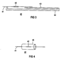
- FIGs 3 and 4 are exemplary embodiments of such a compensation element 40 shown, the one specifically according to the desired Temperature-dependent modeled structure. If necessary can simulate the desired temperature dependency also done in sections with linearized approximations.
- At least the part is a Optical fiber 41, in which a fiber Bragg grating 42 is arranged is housed in a housing.
- the optical fiber 41 is in the area of the fiber Bragg grating 42 between two housing parts 43 and 44 arranged. Both housing parts 43 and 44 have a different temperature expansion on.
- the housing part 43 is made of one material with large thermal expansion and the housing part 44 made of a material with low thermal expansion.
- the housing parts 43 and 44 can thus be a temperature T dependent reflection behavior of the fiber Bragg grating 42 set.
- the compensation element 40 with the fiber Bragg grating arranged in the optical waveguide 41 42 instead of a housing also a coating 46 exhibit.
- the coating 46 is selected such that the Disturbance variable a wave change ⁇ in the desired type and Way.
- a combination of the two embodiments of Figures 3 and 4 is also possible. So it can also be a coated one and optical waveguide 41 arranged in a housing is used become.
- the design of the compensation element is an example below 40 for a magnetic field or current sensitive optical sensor 50 explained.
- the measurement sensitivity is in this type of sensor by the so-called Verdet constant certainly.
- the Verdet constant doesn't just show one Dependence on the quantity to be detected, here the magnetic field, but also a dependency on the one to be compensated Disturbance, here the temperature, as well as the wavelength ⁇ of the fed light signal S1.
- the temperature dependence of the Verdet constant is in the temperature application range of the sensor 50 to approximately between 0.01% / ° C and 0.02% / ° C. It is considered in the here Temperature range between -40 ° C and + 80 ° C one linear temperature dependence of the Verdet constant assumed. The measurement result shows over the entire temperature range ⁇ T of 120 ° C then a temperature-related deviation from between ⁇ 0.6% and ⁇ 1.2%. This unwanted influence it is necessary to compensate.
- the wavelength dependence of the Verdet constant is, for example, -0.0003% / pm (see “Verdet Constant Dispersion in Annealed Optical Fiber Current Sensors" by A.H. Rose et al., Journal of Lightwave Technology, Vol. 15, No. 5, 1997 , Rarely 803 to 807 ).
- the compensation element 40 should therefore have a wavelength-dependent change in wavelength of between 33 pm / ° C and 66 pm / ° C.
- a wave change of between 4 nm and 8 nm then results over the entire temperature range ⁇ T of 120 ° C., the fiber Bragg grating 42 used in the example considered here having a focal wavelength of approximately 850 nm.
- the natural temperature dependence of the wavelength shift in the fiber Bragg grating 42 is of the order of magnitude of about 6.5 pm / ° C, that is too low compared to the value required for compensation between 33 pm / ° C and 66 pm / ° C.
- the temperature dependence is therefore increased by using an appropriate coating 46.
- an appropriate coating 46 For example, when using the polymer described in "Enhanced pressure and temperature sensitivity of a fiber Bragg grating with polymer packaging" by Y. Liu et al., SPIE, Vol. 3740, 1999, pages 284 to 287 as the material for the coating 46 with 50 pm / ° C a value is reached that is in the range between 33 pm / ° C and 66 pm / ° C. Accordingly, another required change in wavelength in the compensation element 40 due to the temperature or another disturbance variable to be compensated can be achieved with a different coating material.
Landscapes
- Physics & Mathematics (AREA)
- General Physics & Mathematics (AREA)
- Optical Transform (AREA)
- Indication And Recording Devices For Special Purposes And Tariff Metering Devices (AREA)
- Measuring Magnetic Variables (AREA)
- Measuring Instrument Details And Bridges, And Automatic Balancing Devices (AREA)
- Instruments For Measurement Of Length By Optical Means (AREA)
Abstract
Description
- das Lichtsignal auch in einem Kompensationselement, das sich zusammen mit dem optischen Sensor in auf einem gemeinsamen Störgrößeneinwirkungsbereich mit weitgehend gleicher Einwirkung der Störgröße auf den optischen Sensor und auf das Kompensationselement befindet, eingespeist wird und
- bei der Passage durch das Kompensationselement unter dem Einfluss der Störgröße in seiner Wellenlänge derart verändert wird, dass
- sich die im optischen Sensor erfolgenden Teilbeeinflussungen aufgrund der veränderten Wellenlänge und aufgrund der Störgröße zumindest weitgehend gegenseitig aufheben.
- ein ebenfalls von dem Lichtsignal durchlaufenes Kompensationselement, das sich zusammen mit dem optischen Sensor in einem gemeinsamen Störgrößeneinwirkungsbereich mit weitgehend gleicher Einwirkung der Störgröße auf den optischen Sensor und das Kompensationselement befindet,
- wobei das Kompensationselement so ausgestaltet ist, dass eine bei der Passage des Lichtsignals durch das Kompensationselement unter dem Störgrößeneinfluss hervorgerufene Wellenlängenänderung bei der anschließenden Passage des in seiner Wellenlänge veränderten Lichtsignals durch den optischen Sensor zu einer wellenlängenabhängigen Teilbeeinflussung führt, die zumindest weitgehend eine störgrößenabhängige Teilbeeinflussung im optischen Sensor kompensiert.
- Figur 1 und 2
- jeweils eine Vorrichtungsanordnung zur störgrößenkompensierten optischen Messwerterfassung mittels eines Kompensationselements
- Figur 3
- ein Kompensationselement mit Gehäuse für einen Einsatz in den Vorrichtungen gemäß Figur 1 oder 2 und
- Figur 4
- ein Kompensationselement mit Beschichtung für einen Einsatz in den Vorrichtungen gemäß Figur 1 oder 2.

Claims (8)
- Verfahren zur Störgrößenkompensation eines optischen Sensors (50, 55), bei dema) ein Lichtsignal (S1) im optischen Sensor (50, 55) mindestens in Abhängigkeit von einer zu detektierenden Messgröße (M), von einer Wellenlänge (λ) des eingespeisten Lichtsignals (S1) und von einer Störgröße (T, V) beeinflusst wird,
dadurch gekennzeichnet, dassb) das Lichtsignal (S1) auch in ein Kompensationselement (40, 45), das sich zusammen mit dem optischen Sensor (50, 55) in einem gemeinsamen Störgrößeneinwirkungsbereich (60, 65) mit weitgehend gleicher Einwirkung der Störgröße (T, V) auf den optischen Sensor (50, 55) und auf das Kompensationselement (40, 45) befindet, eingespeist wird undc) bei der Passage durch das Kompensationselement (40, 45) unter dem Einfluss der Störgröße (T, V) in seiner Wellenlänge derart verändert wird, dassd) sich die im optischen Sensor (50, 55) erfolgenden Teilbeeinflussungen aufgrund der veränderten Wellenlänge und aufgrund der Störgröße (T, V) zumindest weitgehend gegenseitig aufheben. - Verfahren nach Anspruch 1, bei dem das Lichtsignal (S1) in einem als Bragg-Gitter (40, 45) ausgebildeten Kompensationselement in seiner Wellenlänge verändert wird.
- Verfahren nach Anspruch 1 oder 2, bei dem im optischen Sensor (50, 55) die störgrößenabhängige Teilbeeinflussung des Lichtsignals (S1) durch eine Temperatur (T) oder eine Vibration (V) hervorgerufen wird.
- Vorrichtung zur Störgrößenkompensation eines optischen Sensors (50, 55), wobeia) der von einem Lichtsignal (S1) durchlaufene optische Sensor (50, 55) mindestens empfindlich gegenüber einer Messgröße (M), einer Wellenlänge (λ) des Lichtsignals (S1) und einer Störgröße (T, V) ist,
gekennzeichnet durchb) ein ebenfalls von dem Lichtsignal (S1) durchlaufenes Kompensationselement (40, 45), das sich zusammen mit dem optischen Sensor (50, 55) in einem gemeinsamen Störgrößeneinwirkungsbereich (60, 65) mit weitgehend gleicher Einwirkung der Störgröße (T, V) auf den optischen Sensor (50, 55) und das Kompensationselement (40, 45) befindet,c) wobei das Kompensationselement (40, 45) so ausgestaltet ist, dass eine bei der Passage des Lichtsignals (S1) durch das Kompensationselement (40, 45) unter dem Störgrößeneinfluss hervorgerufene Wellenlängenänderung (Δλ) bei der anschließenden Passage des Lichtsignals (S1) durch den optischen Sensor (50, 55) zu einer wellenlängenabhängigen Teilbeeinflussung führt, die zumindest weitgehend eine störgrößenabhängige Teilbeeinflussung im optischen Sensor (50, 55) kompensiert. - Vorrichtung nach Anspruch 4, bei der das Kompensationselement als Bragg-Gitter (40, 45) ausgebildet ist.
- Vorrichtung nach Anspruch 4 oder 5, bei der das Kompensationselement (40, 45) ausgelegt ist für eine in Form einer Temperatur (T) oder einer Vibration (V) vorliegenden Störgröße.
- Vorrichtung nach einem der Ansprüche 4 bis 6, bei der das Kompensationselement (40, 45) ein Gehäuse (43, 44) umfasst, und die Ausgestaltung des Gehäuses (43, 44) mit dazu beiträgt, dass die Wellenlängenänderung (Δλ) unter dem Einfluss der Störgröße (T, V) in vorbestimmter Weise erfolgt.
- Vorrichtung nach einem der Ansprüche 4 bis 7, bei der das Kompensationselement (40, 45) eine Beschichtung (46) umfasst.
Applications Claiming Priority (2)
| Application Number | Priority Date | Filing Date | Title |
|---|---|---|---|
| DE10140482 | 2001-08-17 | ||
| DE10140482A DE10140482B4 (de) | 2001-08-17 | 2001-08-17 | Verfahren und Vorrichtung zur Störgrößenkompensation eines optischen Sensors |
Publications (3)
| Publication Number | Publication Date |
|---|---|
| EP1284425A2 true EP1284425A2 (de) | 2003-02-19 |
| EP1284425A3 EP1284425A3 (de) | 2004-07-14 |
| EP1284425B1 EP1284425B1 (de) | 2007-05-30 |
Family
ID=7695821
Family Applications (1)
| Application Number | Title | Priority Date | Filing Date |
|---|---|---|---|
| EP02017487A Expired - Fee Related EP1284425B1 (de) | 2001-08-17 | 2002-08-05 | Verfahren und Vorrichtung zur Störgrössenkompensation eines optischen Sensors |
Country Status (5)
| Country | Link |
|---|---|
| US (1) | US7064315B2 (de) |
| EP (1) | EP1284425B1 (de) |
| JP (1) | JP4472239B2 (de) |
| CN (1) | CN1250974C (de) |
| DE (2) | DE10140482B4 (de) |
Cited By (2)
| Publication number | Priority date | Publication date | Assignee | Title |
|---|---|---|---|---|
| WO2011116899A1 (de) * | 2010-03-26 | 2011-09-29 | Karlsruher Institut für Technologie | Massenstromsensor und verfahren zur bestimmung des massenstroms in einem rohr |
| US8810132B2 (en) | 2010-03-26 | 2014-08-19 | E2V Technologies (Uk) Limited | Magnetron |
Families Citing this family (7)
| Publication number | Priority date | Publication date | Assignee | Title |
|---|---|---|---|---|
| EP1462811A1 (de) * | 2003-03-28 | 2004-09-29 | Abb Research Ltd. | Elektrooptischer Spannungssensor für hohe Spannungen |
| EP1462810B1 (de) * | 2003-03-28 | 2015-09-09 | ABB Research Ltd. | Temperaturkompensierter elektrooptischer Spannungssensor |
| GB201112161D0 (en) * | 2011-07-15 | 2011-08-31 | Qinetiq Ltd | Portal monitoring |
| DE112014003851B4 (de) * | 2013-08-22 | 2020-12-24 | Leoni Kabel Gmbh | Sensorbaueinheit |
| CN106030318B (zh) | 2013-12-20 | 2020-11-17 | Abb电网瑞士股份公司 | 光纤传感器和方法 |
| DE102014103721A1 (de) * | 2013-12-20 | 2015-06-25 | Endress + Hauser Conducta Gesellschaft für Mess- und Regeltechnik mbH + Co. KG | Optischer Sensor, insbesondere zur Bestimmung von Stoffkonzentrationen in wässrigen Lösungen mittels einer Chemilumineszenz-, Absorptions- oder Fluoreszenzmessung |
| CN105403763A (zh) * | 2015-11-02 | 2016-03-16 | 国家电网公司 | 一种光纤电流传感器费尔德常数温度补偿方法及装置 |
Citations (8)
| Publication number | Priority date | Publication date | Assignee | Title |
|---|---|---|---|---|
| GB1353543A (en) * | 1970-06-09 | 1974-05-22 | Bbc Brown Boveri & Cie | Electro-optical apparatus for rotating the plane of polarisation of a plane polarised light wave |
| US4002975A (en) * | 1976-02-26 | 1977-01-11 | The United States Of America As Represented By The Secretary Of The Interior | Electro-optic measurement of voltage on high-voltage power lines |
| US4269483A (en) * | 1978-10-19 | 1981-05-26 | Siemens Aktiengesellschaft | Electro-optical voltage measurement device |
| EP0390581A2 (de) * | 1989-03-31 | 1990-10-03 | Ngk Insulators, Ltd. | Instrument zur gleichzeitigen optischen Messung von thermischen und elektrischen Grössen |
| WO1995010046A1 (de) * | 1993-10-01 | 1995-04-13 | Siemens Aktiengesellschaft | Verfahren und vorrichtung zum messen einer elektrischen wechselgrösse mit temperaturkompensation |
| WO1996012195A1 (de) * | 1994-10-12 | 1996-04-25 | Siemens Aktiengesellschaft | Optisches messverfahren und optische messvorrichtung zum messen einer elektrischen wechselspannung oder eines elektrischen wechselfeldes mit temperaturkompensation |
| US5764046A (en) * | 1993-04-14 | 1998-06-09 | Siemens Atkiengesellschaft | Optical method and device for measuring an alternating electrical current with temperature compensation |
| US6016702A (en) * | 1997-09-08 | 2000-01-25 | Cidra Corporation | High sensitivity fiber optic pressure sensor for use in harsh environments |
Family Cites Families (8)
| Publication number | Priority date | Publication date | Assignee | Title |
|---|---|---|---|---|
| US5042898A (en) * | 1989-12-26 | 1991-08-27 | United Technologies Corporation | Incorporated Bragg filter temperature compensated optical waveguide device |
| US5394488A (en) * | 1993-11-30 | 1995-02-28 | United Technologies Corporation | Optical fiber grating based sensor |
| AU5385198A (en) * | 1996-12-03 | 1998-07-15 | Micron Optics, Inc. | Temperature compensated fiber bragg gratings |
| US6181851B1 (en) * | 1997-05-29 | 2001-01-30 | E-Tek Dynamics, Inc. | Temperature-compensated optical fiber package |
| IT1305113B1 (it) * | 1998-12-21 | 2001-04-10 | Cselt Centro Studi Lab Telecom | Dispositivo a reticolo di bragg in fibra ottica con compensazionepassiva della temperatura. |
| DE19860409A1 (de) * | 1998-12-28 | 2000-06-29 | Abb Research Ltd | Faser-Bragg-Gitter Sensor zur Messung differentieller Drücke und von Strömungsgeschwindigkeiten |
| DE19938978A1 (de) * | 1999-08-19 | 2001-02-22 | Abb Research Ltd | Faseroptischer Drucksensor |
| US6477309B2 (en) * | 2000-06-13 | 2002-11-05 | Bti Photonics Inc. | Temperature-compensating arrangements and methods for optical fiber |
-
2001
- 2001-08-17 DE DE10140482A patent/DE10140482B4/de not_active Expired - Fee Related
-
2002
- 2002-08-05 EP EP02017487A patent/EP1284425B1/de not_active Expired - Fee Related
- 2002-08-05 DE DE50210224T patent/DE50210224D1/de not_active Expired - Lifetime
- 2002-08-16 JP JP2002237425A patent/JP4472239B2/ja not_active Expired - Fee Related
- 2002-08-19 US US10/222,786 patent/US7064315B2/en not_active Expired - Fee Related
- 2002-08-19 CN CNB02130596XA patent/CN1250974C/zh not_active Expired - Fee Related
Patent Citations (8)
| Publication number | Priority date | Publication date | Assignee | Title |
|---|---|---|---|---|
| GB1353543A (en) * | 1970-06-09 | 1974-05-22 | Bbc Brown Boveri & Cie | Electro-optical apparatus for rotating the plane of polarisation of a plane polarised light wave |
| US4002975A (en) * | 1976-02-26 | 1977-01-11 | The United States Of America As Represented By The Secretary Of The Interior | Electro-optic measurement of voltage on high-voltage power lines |
| US4269483A (en) * | 1978-10-19 | 1981-05-26 | Siemens Aktiengesellschaft | Electro-optical voltage measurement device |
| EP0390581A2 (de) * | 1989-03-31 | 1990-10-03 | Ngk Insulators, Ltd. | Instrument zur gleichzeitigen optischen Messung von thermischen und elektrischen Grössen |
| US5764046A (en) * | 1993-04-14 | 1998-06-09 | Siemens Atkiengesellschaft | Optical method and device for measuring an alternating electrical current with temperature compensation |
| WO1995010046A1 (de) * | 1993-10-01 | 1995-04-13 | Siemens Aktiengesellschaft | Verfahren und vorrichtung zum messen einer elektrischen wechselgrösse mit temperaturkompensation |
| WO1996012195A1 (de) * | 1994-10-12 | 1996-04-25 | Siemens Aktiengesellschaft | Optisches messverfahren und optische messvorrichtung zum messen einer elektrischen wechselspannung oder eines elektrischen wechselfeldes mit temperaturkompensation |
| US6016702A (en) * | 1997-09-08 | 2000-01-25 | Cidra Corporation | High sensitivity fiber optic pressure sensor for use in harsh environments |
Non-Patent Citations (1)
| Title |
|---|
| MITSUI T ET AL: "DEVELOPMENT OF FIBER-OPTIC VOLTAGE SENSORS AND MAGNETIC-FIELD SENSORS" IEEE TRANSACTIONS ON POWER DELIVERY, IEEE INC. NEW YORK, US, Bd. PWRD-2, Nr. 1, Januar 1987 (1987-01), Seiten 87-93, XP009023787 ISSN: 0885-8977 * |
Cited By (2)
| Publication number | Priority date | Publication date | Assignee | Title |
|---|---|---|---|---|
| WO2011116899A1 (de) * | 2010-03-26 | 2011-09-29 | Karlsruher Institut für Technologie | Massenstromsensor und verfahren zur bestimmung des massenstroms in einem rohr |
| US8810132B2 (en) | 2010-03-26 | 2014-08-19 | E2V Technologies (Uk) Limited | Magnetron |
Also Published As
| Publication number | Publication date |
|---|---|
| EP1284425B1 (de) | 2007-05-30 |
| CN1250974C (zh) | 2006-04-12 |
| EP1284425A3 (de) | 2004-07-14 |
| JP4472239B2 (ja) | 2010-06-02 |
| DE10140482B4 (de) | 2008-11-13 |
| DE10140482A1 (de) | 2003-03-13 |
| CN1407343A (zh) | 2003-04-02 |
| JP2003084014A (ja) | 2003-03-19 |
| DE50210224D1 (de) | 2007-07-12 |
| US20030034768A1 (en) | 2003-02-20 |
| US7064315B2 (en) | 2006-06-20 |
Similar Documents
| Publication | Publication Date | Title |
|---|---|---|
| EP1190262B1 (de) | Bragg-gitter-vorrichtung zur messung einer beschleunigung | |
| EP3097397B1 (de) | Schienenmesssystem | |
| DE60225023T2 (de) | Bestimmung einer optischen Eigenschaft unter Benutzung von überlagerten und verzögerten Signalen | |
| DE3609507C2 (de) | Faseroptisches Interferometer | |
| EP2478599B1 (de) | Wellenlängenabstimmbare lichtquelle | |
| EP0795121A1 (de) | Verfahren und vorrichtung zur messung von lichtbündeln | |
| DE60014631T2 (de) | Dehnungsmessung | |
| EP2856096B1 (de) | Optisches messsystem mit polarisationskompensation, sowie entsprechendes verfahren | |
| DE69828788T2 (de) | Integriertes optisches wellenleiterbauelement | |
| EP2856097B1 (de) | Verfahren zur kompensation von faseroptischen messsystemen und faseroptisches messsystem | |
| DE4023175A1 (de) | Verfahren und vorrichtung zum gewinnen von daten zur bestimmung der dauer und frequenzmodulation von ultrakurzen laserpulsen | |
| DE60118871T2 (de) | Lichtwellenlängenmessvorrichtung und Verfahren unter Verwendung eines Zweistrahlinterferometers | |
| EP1284425B1 (de) | Verfahren und Vorrichtung zur Störgrössenkompensation eines optischen Sensors | |
| DE10037501C1 (de) | Verfahren und Vorrichtung zur Wellenlängendetektion | |
| EP2279397A1 (de) | Vorrichtung zurortsaufgelösten temperaturmessung | |
| DE3812334A1 (de) | Interferometrische einrichtung | |
| EP2318806A1 (de) | FASEROPTISCHES INTERFEROMETER UND VERFAHREN ZUR BESTIMMUNG PHYSIKALISCHER ZUSTANDSGRÖßEN IM INNERN EINER FASERSPULE EINES FASEROPTISCHEN INTERFEROMETERS | |
| EP3088844B1 (de) | Faseroptisches system und verfahren zur reduktion von biasfehlern in einem solchen faseroptischen system | |
| EP0529339B1 (de) | Faseroptischer Sensor | |
| EP1141663A1 (de) | Fibre bragg grating sensors for measuring a physical magnitude | |
| EP0241766A2 (de) | Sensoranordnung | |
| EP3401634A1 (de) | Abstandsmessanordnung zur bestimmung eines abstandes zu einem objekt | |
| DE112014003851B4 (de) | Sensorbaueinheit | |
| DE69817131T2 (de) | Interferometer zu Messung optischer Eigenschaften in Proben | |
| DE10112835B4 (de) | Verfahren und Einrichtung zur Strommessung mittels eines faseroptischen In-Line-Sagnac-Interferometers und dafür geeigneter Phasenmodulator |
Legal Events
| Date | Code | Title | Description |
|---|---|---|---|
| PUAI | Public reference made under article 153(3) epc to a published international application that has entered the european phase |
Free format text: ORIGINAL CODE: 0009012 |
|
| AK | Designated contracting states |
Designated state(s): AT BE BG CH CY CZ DE DK EE ES FI FR GB GR IE IT LI LU MC NL PT SE SK TR |
|
| AX | Request for extension of the european patent |
Extension state: AL LT LV MK RO SI |
|
| PUAL | Search report despatched |
Free format text: ORIGINAL CODE: 0009013 |
|
| AK | Designated contracting states |
Kind code of ref document: A3 Designated state(s): AT BE BG CH CY CZ DE DK EE ES FI FR GB GR IE IT LI LU MC NL PT SE SK TR |
|
| AX | Request for extension of the european patent |
Extension state: AL LT LV MK RO SI |
|
| RIC1 | Information provided on ipc code assigned before grant |
Ipc: 7G 02F 1/065 B Ipc: 7G 01R 29/08 B Ipc: 7G 02F 1/061 B Ipc: 7G 01R 1/07 B Ipc: 7G 01R 15/24 A Ipc: 7G 02F 1/03 B |
|
| 17P | Request for examination filed |
Effective date: 20040804 |
|
| AKX | Designation fees paid |
Designated state(s): DE FR GB IT |
|
| 17Q | First examination report despatched |
Effective date: 20050401 |
|
| GRAP | Despatch of communication of intention to grant a patent |
Free format text: ORIGINAL CODE: EPIDOSNIGR1 |
|
| GRAS | Grant fee paid |
Free format text: ORIGINAL CODE: EPIDOSNIGR3 |
|
| GRAA | (expected) grant |
Free format text: ORIGINAL CODE: 0009210 |
|
| AK | Designated contracting states |
Kind code of ref document: B1 Designated state(s): DE FR GB IT |
|
| REG | Reference to a national code |
Ref country code: GB Ref legal event code: FG4D Free format text: NOT ENGLISH |
|
| REF | Corresponds to: |
Ref document number: 50210224 Country of ref document: DE Date of ref document: 20070712 Kind code of ref document: P |
|
| GBT | Gb: translation of ep patent filed (gb section 77(6)(a)/1977) |
Effective date: 20070704 |
|
| ET | Fr: translation filed | ||
| PLBE | No opposition filed within time limit |
Free format text: ORIGINAL CODE: 0009261 |
|
| STAA | Information on the status of an ep patent application or granted ep patent |
Free format text: STATUS: NO OPPOSITION FILED WITHIN TIME LIMIT |
|
| 26N | No opposition filed |
Effective date: 20080303 |
|
| PGFP | Annual fee paid to national office [announced via postgrant information from national office to epo] |
Ref country code: GB Payment date: 20120809 Year of fee payment: 11 |
|
| PGFP | Annual fee paid to national office [announced via postgrant information from national office to epo] |
Ref country code: IT Payment date: 20120824 Year of fee payment: 11 Ref country code: FR Payment date: 20120823 Year of fee payment: 11 |
|
| PGFP | Annual fee paid to national office [announced via postgrant information from national office to epo] |
Ref country code: DE Payment date: 20121019 Year of fee payment: 11 |
|
| GBPC | Gb: european patent ceased through non-payment of renewal fee |
Effective date: 20130805 |
|
| PG25 | Lapsed in a contracting state [announced via postgrant information from national office to epo] |
Ref country code: DE Free format text: LAPSE BECAUSE OF NON-PAYMENT OF DUE FEES Effective date: 20140301 |
|
| REG | Reference to a national code |
Ref country code: FR Ref legal event code: ST Effective date: 20140430 |
|
| PG25 | Lapsed in a contracting state [announced via postgrant information from national office to epo] |
Ref country code: IT Free format text: LAPSE BECAUSE OF NON-PAYMENT OF DUE FEES Effective date: 20130805 |
|
| REG | Reference to a national code |
Ref country code: DE Ref legal event code: R119 Ref document number: 50210224 Country of ref document: DE Effective date: 20140301 |
|
| PG25 | Lapsed in a contracting state [announced via postgrant information from national office to epo] |
Ref country code: GB Free format text: LAPSE BECAUSE OF NON-PAYMENT OF DUE FEES Effective date: 20130805 |
|
| PG25 | Lapsed in a contracting state [announced via postgrant information from national office to epo] |
Ref country code: FR Free format text: LAPSE BECAUSE OF NON-PAYMENT OF DUE FEES Effective date: 20130902 |