TECHNICAL FIELD
-
The present invention relates to a method for precision-processing
a fine structure. More particularly, the present
invention relates to a method capable of productively forming
uniform, ultrafine structures with a size of about several
tens of micrometers on the industrial scale.
BACKGROUND ART
-
Currently, the electronics industry sees a rapid
progress of semiconductor devices. Integration of the
elements is improved as the dimensions of the semiconductor
devices are reduced. Accordingly, various efforts have been
made to fabricate ultrafine devices.
-
Conventionally, fabrication of submicron devices is
implemented by downsizing the normal transistors. This
downsizing is based on the lithography technology.
-
More specifically, a resist film, which is capable of
being modified by light, X-rays, electron beams or the like,
is applied to a substrate. A reticle (photomask) having an
appropriate pattern is then placed thereon. Light, X-rays,
electron beams or the like is radiated through the reticle in
order to modify the resist film. Either the modified or
unmodified resist film is then removed to form a resist
pattern on the substrate.
-
On the other hand, the semiconductor industry shows the
possibilities of a quantum effect element in a semiconductor
region having a size of several tens of nanometers because of
its excellent functionality. Accordingly, establishment of
the processing technology for forming ultrafine structures
with a size of several tens of nanometers or less has been
demanded in the semiconductor industry.
-
However, there is a limit in the lithography technology
in terms of accuracy for the following reasons: photomask
alignment error cannot be eliminated; there is a limit in the
technology of reducing the mask size; and a resist material
is not capable of being modified in a satisfactory manner by
light or the like. Accordingly, the lithography technology
is problematic in forming fine structures having a size of
several tens of nanometers.
-
Various efforts have been made to solve the above
problems like using the self-alignment technology to minimize
the use of the lithography process. However, even these
methods do not completely solve the problems in forming the
uniform, fine structures.
PROBLEMS
-
Accordingly, it is a prime task in the field of
ultrafine semiconductor devices with a size of several tens
of nanometers or less to develop a method capable of
accurately processing a fine structure in a manner suitable
for mass production, which is heretofore impossible. For
practical applications of the semiconductor devices, the
produced fine structures are required to have a uniform size.
-
The present invention is made to solve the above
problems, and it is an object of the present invention to
propose a method capable of accurately processing a fine
structure in a manner suitable for mass production.
DISCLOSURE OF THE INVENTION
-
It is an object of the present invention to provide a
method for accurately processing a fine structure in a manner
suitable for mass production in the field of ultrafine
semiconductor devices with a size of several tens of
nanometers or less.
-
According to a first aspect of the present invention, a
method for precision-processing a fine structure includes the
steps of: (a) arranging organic molecules on a substrate, the
organic molecules each holding a fine particle in a holding
portion capable of holding a fine particle therein; and (b)
etching the substrate by using at least the fine particles as
an etching mask.
-
Since the substrate can be etched by using the fine
particles arranged on the substrate as a mask, fine
structures having the same size as that of the organic
molecules or fine particles can be formed. The fine
structures thus obtained go beyond the limit of the
lithography technology.
-
In the above method of the first aspect of the present
invention, the organic molecules may include a protein, and
the fine particles may include an inorganic substance. This
enables the organic molecules to be easily removed while
leaving the inorganic substance on the substrate in the step
of removing the organic molecules described below.
-
Preferably, the above method of the first aspect of the
present invention further includes the step of removing the
organic molecules to leave the fine particles on the
substrate, and the removing step is conducted between the
steps (a) and (b). In the step (b), etching is preferably
conducted by using the fine particles as an etching mask.
-
Since the fine particles smaller than the organic
molecules can be used as an etching mask, finer structures
can be formed on the substrate.
-
In the above method of the first aspect of the present
invention, the organic molecules may be ferritin. In this
case, the organic molecules holding fine particles of a
uniform size can be arranged and fixed on the substrate,
enabling formation of uniform fine structures with a high
density. This also facilitates positional control of the
fine structures.
-
The above method of the first aspect of the present
invention may further include the step of (a') causing the
organic molecules to hold the fine particles in a liquid, and
the step (a') is conducted before the step (a). This ensures
that the organic molecules hold the fine particles with a
desired size. As a result, a desired pattern can be formed
in a satisfactory manner.
-
In the above method of the first aspect of the present
invention, the organic molecules before holding the fine
particles may be apoferritin.
-
This facilitates control of introduction of the fine
particles into apoferritin, whereby the concentration of the
fine particles to be applied to the liquid in the subsequent
step (a') can be held at an appropriate value.
-
In the above method of the first aspect of the present
invention, the number of moles of atoms of the fine particles
contained in the liquid is preferably in the range from the
maximum number of moles of the atoms of the fine particles
that can be held by the apoferritin contained in the liquid
to ten times the maximum number of moles.
-
This suppresses production of by-products in the step
(a'), whereby apoferritin holding the fine particles can be
obtained at a high purity.
-
In the above method of the first aspect of the present
invention, the number of moles of atoms of the fine particles
contained in the liquid is more preferably in the range from
the maximum number of moles of the atoms of the fine
particles that can be held by the apoferritin contained in
the liquid to twice the maximum number of moles.
-
This suppresses production of by-products in the step
(a') in a more effective manner, whereby apoferritin holding
the fine particles can be obtained at a higher purity.
-
In the above method of the first aspect of the present
invention, the organic molecules may be bacterial flagellar
filaments, and the fine particles may be a bar-shaped
substance.
-
This enables fine, bar-shaped structures to be formed in
the step (b).
-
In the above method of the first aspect of the present
invention, precision processing of the substrate may be
conducted by a method selected from ion reactive etching, X-ray
radiation, corpuscular radiation, electron beam radiation
and plasma radiation. In this case, the substrate is
effectively etched, enabling formation of fine particles.
-
According to a second aspect of the present invention, a
method for precision-processing a fine structure includes the
steps of: (a) forming a resist film on a substrate; (b)
arranging organic molecules on the resist film on the
substrate, the organic molecules each holding a fine particle
in a holding portion capable of holding a fine particle
therein; (c) patterning the resist film by using at least the
fine particles as a mask to form a resist pattern; and (d)
etching the substrate by using the resist pattern as a mask.
-
Since the fine particles, organic molecules or the like
can be used as a resist mask, etching the substrate according
to the resist pattern enables fine structures to be formed on
the substrate. Moreover, it is possible to etch the
substrate even if the fine particles are not capable of
serving as an etching mask for etching the substrate.
-
According to a third aspect of the present invention, a
method for precision-processing a fine structure includes the
steps of: (a) arranging organic molecules on at least a part
of a substrate; (b) causing a substance to adhere to a
surface of fine particles, the substance having a property to
bond with the organic molecules arranged on the substrate;
(c) causing the substance to bond with the organic molecules;
and (d) etching the substrate by using at least the fine
particles as an etching mask.
-
In the above method, the substance selectively bonds
with the organic compound on the substrate in the step (c),
whereby the particles having the substance thereon are
arranged and fixed on the substrate. In the step (d), the
substrate is etched by using the fine particles arranged on
the substrate with the substance interposed therebetween as
an etching mask. As a result, fine structures can be formed
on the substrate.
-
According to a fourth aspect of the present invention, a
method for precision-processing a fine structure includes the
steps of: (a) arranging organic molecules on a substrate, the
organic molecules holding no fine particle in their
respective holding portions capable of holding a fine
particle therein; and (b) immersing the substrate in a liquid
having the fine particles dispersed therein to introduce the
fine particles into the respective holding portions of the
organic molecules.
-
This enables the fine particles to be effectively
arranged on the substrate.
-
The above method of the fourth aspect of the present
invention may further include the step of (c) etching the
substrate by using at least the fine particles as an etching
mask. Accordingly, the substrate can be etched by using the
particles, organic molecules or the like as an etching mask,
enabling fine structures to be formed on the substrate.
-
In the above method of the fourth aspect of the present
invention, the organic molecules may be apoferritin. This
enables the organic molecules to be arranged and fixed on the
substrate with a high density and also enables fine particles
with a uniform size to be held in the organic molecules. As
a result, uniform, fine structures can be formed with a high
density.
-
In the above method of the fourth aspect of the present
invention, a voltage may be applied to the substrate in the
step (b). The fine particles are thus electrically attracted
toward the substrate, enabling rapid introduction of the fine
particles into the holding portions of the organic molecules.
BRIEF DESCRIPTION OF THE DRAWINGS
-
- FIG. 1 schematically shows the structure of ferritin;
- FIGs. 2(a) to (d) illustrate a method for two-dimensionally
arranging and fixing ferritin on a substrate
according to first and second embodiments;
- FIGS. 3(a) and (b) are cross-sectional views
illustrating a first specific example of the method for two-dimensionally
arranging and fixing ferritin;
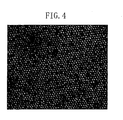
- FIG. 4 shows a scanning electron microscope image of a
two-dimensional crystalline film of ferritin that is arranged
and fixed on the substrate by the method of FIG. 3;
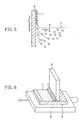
- FIG. 5 is a cross-sectional view illustrating a second
specific example of the method for two-dimensionally
arranging and fixing ferritin;
- FIG. 6 is a cross-sectional view illustrating a third
specific example of the method for two-dimensionally
arranging and fixing ferritin;
- FIG. 7 is a cross-sectional view illustrating a fourth
specific example of the method for two-dimensionally
arranging and fixing ferritin;
- FIGs. 8(a) to (d) are cross-sectional views illustrating
a method for arranging and fixing fine particles on a
substrate by using an antigen-antibody reaction;
- FIGs. 9(a) to (c) are cross-sectional views illustrating
the step of patterning a fine structure without using a
resist film according to the first embodiment;
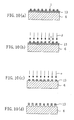
- FIGs. 10(a) to (d) are cross-sectional views
illustrating the step of patterning a fine structure by using
a resist film according to the second embodiment;
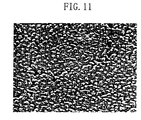
- FIG. 11 is a scanning electron microscope image of fine
columns formed by a method for processing a fine structure
according to the present invention; and
- FIG. 12 is a cross-sectional view of an optical
semiconductor device using fine columns formed by a method
for processing a fine structure according to the present
invention.
-
BEST MODE FOR CARRYING OUT THE INVENTION
- First Embodiment -
-
The first embodiment is a method for precision-processing
a substrate without using a resist film. In this
method, ferritin enclosing iron oxide (hereinafter, the term
"iron oxide" refers to Fe2O3) is arranged on the substrate,
and at least iron oxide dots in the ferritin are used as a
mask. Note that, in every embodiment of the present
invention, the term "substrate" refers to the whole substrate
including structures formed the substrate such as oxide film
and gate electrode.
-
As schematically shown in FIG. 1, ferritin used herein
is a metalloprotein complex formed from a spherical core 1
containing about 3,000 inorganic atoms such as iron, and an
outer shell 2 of twenty-four identical subunits enclosing the
core 1, and each subunit has a molecular weight of about
20,000. Ferritin is found in, e.g., animal liver and spleen
at high level. The outer diameter of ferritin is about 12 nm,
and the diameter of the core 1 held therein is about 6 nm.
Ferritin excluding the core 1 is called "apoferritin", which
includes a holding portion (internal void) for holding the
core therein.
-
The present embodiment is roughly divided into the
following three stages: preparing ferritin enclosing iron
oxide; two-dimensionally arranging and fixing the ferritin on
a substrate; and processing the substrate by using at least
iron oxide dots contained in the ferritin as a mask.
-
A method for introducing iron into apoferritin (ferritin
holding no inorganic substance therein) will be described
first.
-
First, a HEPES buffer solution, an apoferritin solution,
an iron ammonium sulfate (Fe(NH4)2(SO4)2) solution are
sequentially mixed in this order so that the final
concentration is 100 mmol/L (pH 7.0) for the HEPES buffer
solution, 0.5 mg/mL for apoferritin, and 5 mmol/L for iron
ammonium sulfate. Note that the concentration of iron
ammonium sulfate used herein is preferably in the range of 5
to 10 mmol/L, as described below. The operation for
preparing ferritin is entirely conducted at room temperature.
-
As soon as the above solution is prepared, iron ions are
oxidized within apoferritin into brown iron oxide. The
solution is left at rest overnight in order to complete
introduction of the iron ions into apoferritin and oxidation
reaction of the iron thus introduced. As a result, iron
oxide having a uniform size is introduced into the holding
portions of apoferritin, whereby ferritin is produced.
-
Thereafter, a solution containing the ferritin is put
into a container, and centrifuged at 3,000 rpm for 15 to 30
minutes with a centrifugal separator to remove precipitation.
After removing the precipitation, the supernatant liquid is
further centrifuged at 10,000 rpm for 30 minutes to remove a
precipitated aggregate of ferritin.
-
A solvent in the resultant supernatant liquid, i.e., the
100-mmol/L HEPES buffer solution of pH 7.0, is replaced with
a 150-mmol/L NaCl solution. In this step, pH adjustment is
not especially required.
-
The ferritin solution is then concentrated to 1 to 10
mg/mL by dialysis, and CdSO4 is added to the resultant
solution so that the final concentration is 10 mmol/L.
Ferritin is thus aggregated.
-
The solution is then centrifuged at 3,000 rpm for 20
minutes to precipitate the ferritin in the solution. The
buffer components of the solution are replaced with a 10 to
50-mmol/L Tris buffer solution of pH 8.0 containing 150-mmol/L
NaCl by dialysis. The ferritin solution is then
concentrated, and ferritin monomers enclosing iron oxide are
separated from the ferritin solution by a gel filtration
column.
-
If high-concentration iron ammonium sulfate is added to
the ferritin solution as an iron resource in the first stage
of this method, by-products would be produced, which inhibit
high-purity ferritin enclosing iron oxide from being obtained.
It is therefore preferable to use low-concentration iron
ammonium sulfate. However, since 0.5-mg/mL apoferritin
reacts with 3-mmol/L iron ammonium sulfate, 5-mmol/L iron
ammonium sulfate is used in the present embodiment in order
to supply a sufficient amount of iron and to prevent side
reaction.
-
Although iron is used as a dot material to be introduced
into apoferritin in the present embodiment, a substance
serving as an etching mask may be introduced thereinto such
as chromium, manganese, cobalt, nickel, aluminum, tungsten,
zinc, and oxides and hydroxides thereof. Note that the
technology of introducing chromium, manganese, cobalt, nickel,
aluminum, tungsten, zinc, and oxides thereof into apoferritin
has already been reported, and can be applied to the present
invention. For example, in the case of cobalt, inorganic
atoms can be introduced into apoferritin by merely adding
apoferritin to an ammonium solution of cobalt sulfate,
adjusting the pH value to around 8.0, and then adding a small
amount of H2O2 solution. The resultant solution changes from
light red to deep green, producing cores of a cobalt compound
in the holding portions of apoferritin.
-
Regarding other embodiments of the present invention as
well, an inorganic substance such as chromium, manganese,
cobalt, nickel, aluminum, tungsten and zinc may be similarly
introduced into the holding portions of apoferritin.
-
In every embodiment of the present invention,
apoferritin may be the one extracted from an animal organ
such as equine or bovine spleen and liver. However,
apoferritin that is produced within bacteria such as
Escherichia coli by a genetic engineering method is
preferable due to its homogeneity.
-
In the following embodiments, apoferritin is used to
arrange fine particles that serve as a mask for a lithography
process or an etching process. However, other proteins
capable of holding fine particles therein may be used such as
outer shells of viruses such as adenovirus, rotavirus, HK97,
CCMV (i.e., viruses excluding genetic materials), proteins of
ferritin family such as ferritins, Dps protein and MrgA
protein, and bacterial flagellar filament. The bacterial
flagellar filament is formed from a protein called flagellin,
and can be present in a helical form. Fine particles trapped
within the flagellar filament will serve as a columnar mask.
These proteins such as ferritins have slightly different
structures if they are derived from different species.
Therefore, by using these proteins in the present invention,
the size of the fine particles to be held therein can be
varied. Ferritin derived from any organism may be prepared
by the same method as that of the present embodiment.
-
The core size and the protein diameter are different
depending on a protein used. For the Dps protein, the core
diameter is 4 nm, the outer shell is a dodecamer of the
protein having a regular tetrahedral structure, and the outer
diameter is 9 nm. Since the shape of the outer shell varies
depending on a protein, the shape of the core also varies
depending on a protein. For example, the bacterial flagellar
filament is a helical protein having a columnar void therein.
Therefore, a bar-shaped core is held therein.
-
The use of the proteins having different core sizes and
core shapes enables formation of fine structures having
different shapes.
-
Alternatively, proteins bonding with a single molecule
of a metal such as heme protein bonding with iron and
collagenase bonding with zinc, polysaccharides having a
property to bond with a metal, and the like may be used in
the present invention.
-
The stage of two-dimensionally arranging and fixing
ferritin on the substrate will now be described. The present
embodiment is based on the method described in Japanese Laid-Open
Publication No. 11-45990.
-
FIGS. 2(a) to (d) illustrate a method for two-dimensionally
arranging and fixing ferritin on the substrate.
A buffer solution, pure water and a solution such as a NaCl
solution used herein are those having organic substances
removed therefrom in advance with an ODS column. As a
preparation, a silicon substrate 6 is subjected to an Washer
process (UV ozone process) to remove organic substances from
its surface. The resultant silicon substrate 6 is then left
at rest for twenty-four hours in 2.5% (v/v)
hexamethyldisilazane (HMDS) ((CH3)3SiNHSi(CH3)3) in order to
cover the surface of the silicon substrate 6 with HMDS and
thus to make the silicon substrate 6 have a hydrophobic
property.
-
Instead of silicon, glass, SOI or carbon grid may be
used as a substrate. When a glass substrate is used, the
substrate may be coated with a monomolecular film of nitrogen
fluoride in order to make the substrate have a hydrophobic
property.
-
First, in the step of FIG. 2(a), 2 to 3 µL of 0.6 mg/mL
PBLH (Poly-1-Benzyl-L-histidine) is dropped to the surface of
a buffer solution containing dispersion of ferritin 4
enclosing iron oxide (Fe2O3) (e.g., a 20-mmol/L phosphate
buffer solution of pH 5.8 containing 60-µg/mL ferritin, 20-mmol/L
sodium chloride, and 5 to 10-mmol/L MgCl2 or CaCl2)
(hereinafter, referred to as solution 3). The resultant
solution is then left at room temperature for 2.5 hours. As
a result, a PBLH film 5 is formed at the surface of the
solution.
-
In the step of FIG. 2(b), the solution 3 is raised to
38°C and left for one hour. The solution 3 is then left for
two hours at room temperature. The PBLH film 5 is positively
charged, while the ferritin 4 is negatively charged at pH 5
or more. Therefore, the ferritin 4 adheres to the PBLH film
5 with time, and a two-dimensional crystalline film of the
ferritin 4 is formed on the PBLH film 5.
-
In the step of FIG. 2(c), the silicon substrate 6 is
slowly placed on the PBLH film 5 and held for one minute at
room temperature to transfer the PBLH film 5 and the two-dimensional
crystalline film of the ferritin 4 onto the
silicon substrate 6.
-
Note that, since the PBLH film 5 has a hydrophobic
property, forming hydrophobic and hydrophilic regions of a
prescribed pattern at the surface of the silicon substrate 6
enables the two-dimensional crystalline film of a desired
pattern to be transferred onto the silicon substrate 6 in the
step of FIG. 2(c). The process of forming the hydrophilic
region in the silicon substrate 6 can be conducted by making
ozone generated by ultraviolet radiation in contact with a
part of the substrate.
-
In the step of FIG. 2(d), the silicon substrate 6 is
separated from the surface of the solution 3 and dried. The
two-dimensional crystalline film of the ferritin 4 is thus
arranged and fixed on the silicon substrate 6.
-
The ferritin 4 has a diameter of 12 nm, and the core 1
enclosed therein has a diameter of about 6 nm. Moreover, the
holding portion is located at a fixed position in the
ferritin. Therefore, the method of the present embodiment
enables patterning of a fine structure of nanometer size that
is beyond the limit of the conventional lithography
technology.
-
Hereinafter, the stage (c) of processing the silicon
substrate 6 will be described with reference to FIGs. 9(a) to
(c).
-
In the step of FIG. 9(a), before an RIE process, the
surface of the silicon substrate 6 having the ferritin
arranged thereon is processed in a nitrogen-gas atmosphere at
450°C for one hour to remove the protein outer shells 2. As
a result, only the iron oxide cores 1 are left on the silicon
substrate 6. The step of removing the outer shells 2 may be
omitted. However, removing the protein portion of the
ferritin 4 allows the cores 1 to be arranged in good order on
the silicon substrate 6. More effective patterning can be
achieved by the following etching process.
-
The outer shells 2 may alternatively be removed by
ozonolysis or chemical decomposition using cyanogen bromide
(CNBr).
-
The silicon substrate 6 may then be processed in a
reducing-gas atmosphere such as hydrogen at 400 to 500°C for
about one hour in order to reduce iron oxide of the outer
shells 2 to iron atoms. This reduces the volume of the cores
1, enabling formation of a finer pattern.
-
When the outer shells 2 of the ferritin 4 are not
removed, the silicon substrate 6 having the ferritin 4
arranged thereon is subjected to reactive ion etching (RIE)
for about ten minutes by using SF6 gas in the step of FIG.
9(b). The outer shells 2 and the silicon substrate 4 are
thus selectively removed. When the outer shells 2 were
removed first, the reactive RIE is conducted for five minutes
to selectively remove the silicon substrate 6. This is
because the cores 1 are less susceptible to etching as
compared to the silicon substrate 1 and the outer shells 2.
-
It should be noted that, when a shallow fine structure
is to be formed, the RIE may be conducted for a short time
(within several minutes) without removing the outer shells 2,
in order to use the outer shells 2 as a mask.
-
In the step of FIG. 9(c), as the etching proceeds, the
cores 2 are finally etched away, whereby the silicon
substrate 6 of a desired pattern is left. The present
embodiment thus enables fine patterning to be conducted with
accuracy.
-
Note that, in the present embodiment, the RIE using SF6
is conducted as a means for patterning the substrate.
However, radiation α capable of selectively removing the
substrate may alternatively be directed such as X-rays,
electron beams, plasma or corpuscular rays.
-
In every embodiment of the present invention, various
proteins capable of enclosing fine particles that serve as a
mask in the lithography and etching processes can be used
instead of ferritin. However, ferritins or Dps protein, MrgA
protein, bacterial flagellar filament, outer shells of
various viruses and the like can be mass-produced by a
genetic engineering method. Therefore, the use of these
proteins enables mass production of fine structures on an
industrial basis.
-
FIG. 11 is a scanning electron microscope image of the
substrate surface after the silicon substrate 6 having the
ferritin 4 densely arranged two-dimensionally is processed by
the method of the present embodiment. This image shows that
columnar structures (hereinafter, referred to as fine
columns) are formed on the silicon substrate 6 along the
pattern of the cores 1 arranged on the silicon substrate 6.
-
Since the cores 1 of the ferritin used in the present
embodiment have a diameter of 6 nm, the fine columns formed
on the silicon substrate 6 have a diameter of 6 nm at their
top ends. Moreover, a protein such as ferritin used in the
present invention holds uniformly sized fine particles of
several nanometers in diameter. Therefore, the present
invention enables formation of fine structures with a uniform
size (i.e., precision processing of fine structures) which
cannot heretofore be implemented.
-
Note that, by using the fine columns of about 6 nm in
diameter formed by the present embodiment, fine light-emitting
elements shown in the third embodiment below can be
formed at high density.
- Second Embodiment -
-
The second embodiment is a method for arranging ferritin
enclosing iron oxide onto a substrate having a resist film
thereon, patterning the resist film by using at least iron
oxide dots within the ferritin as a mask, and etching the
substrate using the resist film pattern as a mask.
-
First, ferritin enclosing iron oxide is prepared by the
same method as that of the first embodiment.
-
FIGs. 2(a) to (d) illustrate a method for two-dimensionally
arranging and fixing ferritin on the substrate.
-
A buffer solution, pure water and a solution such as a
NaCl solution used herein are those having organic substances
removed therefrom in advance with an ODS column.
-
As a preparation, a material such as calix arene, a
positive resist, is formed with a thickness of 10 nm on a
silicon substrate to be used. Another positive resist such
as polymethyl methacrylate (PMMA), α-methylstyrene resin and
novolak may be used instead of calix arene. A negative
resist may be used. However, a negative resist is
problematic in terms of etching accuracy. Therefore, a
positive resist is preferred. The resist film may be formed
either by applying a resist material directly on the
substrate or by forming a film of a resist material first and
then laminating the film on the substrate. The thickness of
the resist film is not specifically limited.
-
Like the first embodiment, in the step of FIG. 2(a), 2
to 3 µL of 0.6 mg/mL PBLH is first dropped to the surface of
a buffer solution containing dispersion of ferritin 4
enclosing iron oxide (e.g., a 20-mmol/L phosphate buffer
solution of pH 5.8 containing 60-µg/mL ferritin, 20-mmol/L
sodium chloride, and 5 to 10-mmol/L MgCl2 or CaCl2) (solution
3). The resultant solution is then left at room temperature
for 2.5 hours. As a result, a PBLH film 5 is formed at the
surface of the solution.
-
In the step of FIG. 2(b), the solution is raised to 38°C
and left for one hour. The solution 3 is then left for two
hours at room temperature. The PBLH film 5 is positively
charged, while the ferritin 4 is negatively charged.
Therefore, the ferritin 4 adheres to the PBLH film 5 with
time, and a two-dimensional crystalline film of the ferritin
4 is formed on the PBLH film 5.
-
In the step of FIG. 2(c), the silicon substrate 6 having
the resist film 13 formed thereon is slowly placed on the
PBLH film 5 such that the resist film faces the PBLH film 5.
The silicon substrate 6 is thus held for one minute at room
temperature to transfer the PBLH film 5 and the two-dimensional
crystalline film of the ferritin 4 onto the
silicon substrate 6. Since the resist film 13 on the silicon
substrate has a hydrophobic property, the ferritin 4 is
rapidly transferred onto the surface of the resist film 13 on
the silicon substrate 6. Forming a hydrophilic region of a
prescribed pattern at the surface of the resist film 13 on
the silicon substrate 6 enables the two-dimensional
crystalline film of a desired pattern to be transferred onto
the silicon substrate 6. The process of forming the
hydrophilic region in the resist film 13 is conducted by
making ozone generated by ultraviolet radiation in contact
with a part of the substrate.
-
Alternatively, a positively or negatively charged
substance may be bonded to the surface of the resist film 13
in order to form a desired pattern by the charge difference.
-
For example, ferritin is negatively charged when the
solution has a pH value of 5.0 or more. Therefore,
processing the substrate with a substance that is positively
charged at pH 11 or less such as aminosilane enables the
ferritin to be transferred onto the resist film 13 at pH 5 to
pH 11.
-
In the step of FIG. 2(d), the silicon substrate 6 is
separated from the surface of the solution 3 and dried. The
two-dimensional crystalline film of the ferritin 4 is thus
arranged and fixed on the resist film 13.
-
The ferritin has a diameter of 12 nm, and the core 1
enclosed therein has a diameter of about 6 nm. The holding
portion is located at a fixed position in the ferritin.
Therefore, the present embodiment using the cores 1 as a mask
enables a fine structure of nanometer size to be patterned
with highly improved accuracy over the conventional
lithography technology.
-
Hereinafter, the stage of processing the silicon
substrate 6 will be described with reference to FIGS. 10(a)
to (d).
-
In the step of FIG. 10(a), before an RIE process, the
surface of the silicon substrate 6 having the ferritin 4
arranged thereon is chemically decomposed with cyanogen
bromide (CNBr) to remove the protein outer shells 2. As a
result, only the iron oxide cores 1 are left on the resist
film 13 of the silicon substrate 6. The step of removing the
outer shells 2 may be omitted to conduct a lithography
process by using the outer shells 2 as a mask. However,
removing the protein portion of the ferritin 4 allows the
cores 1 to be arranged in good order on the silicon substrate
6. The outer shells 2 may alternatively be removed by
ozonolysis, and if the resist film 13 has heat resistance, by
thermal decomposition of processing the substrate in a
nitrogen-gas atmosphere at 450°C for one hour.
-
The silicon substrate 6 may then be processed in a
reducing-gas atmosphere such as hydrogen at 400 to 500°C for
about one hour in order to reduce iron oxide of the core 1 to
iron atoms. This reduces the volume of the cores 1, enabling
formation of a finer pattern in later steps.
-
In the step of FIG. 10(b), radiation β such as electron
beams or X-rays is directed downward onto the silicon
substrate 6. The cores 1 on the resist film 13 serve as a
mask, and the resist film 13 on the silicon substrate 6 is
modified into a removable film except for the regions right
under the cores 1.
-
In the step of FIG. 10(c), the surface of the silicon
substrate 6 is washed to remove the cores 1 and the modified
resist film from the silicon substrate 6. An unmodified
resist film 13a is thus left thereon.
-
In the step of FIG. 10(d), RIE using SF6 is conducted by
using the resist film 13a left on the silicon substrate 6 as
a mask, until a desired structure is obtained.
-
Note that, in the present embodiment, the RIE using SF6
is conducted as a means for patterning the substrate.
However, radiation α capable of removing the substrate may
alternatively be directed such as X-rays, electron beams,
plasma or corpuscular rays.
-
The remaining resist film 13 is then washed away with an
appropriate means.
-
The present embodiment also enables accurate formation
of a fine pattern of nanometer size. In other words, the
present embodiment enables formation of fine structures with
a uniform size (i.e., precision processing of fine
structures) which cannot be implemented with the conventional
lithography technology.
- Third Embodiment -
-
In the third embodiment, the method for manufacturing an
optical semiconductor device described in Eriguchi, et al.,
Japanese Laid-Open Publication No. 11-233752 will be
described using the fine columns formed by the method for
precision-processing a fine structure according to the
present invention.
-
FIG. 12 is a cross-sectional view of an optical
semiconductor device using fine semiconductor columns of 6 nm
in diameter formed by the first or second embodiment.
-
In the first and second embodiments, n-type silicon
having a p-well 41 formed therein and an n-well formed on the
p-well 41 is used as a substrate. The substrate is etched to
a depth within the p-well 41, whereby fine semiconductor
columns 32 of n-type silicon are densely formed
perpendicularly to the substrate surface.
-
The side surfaces of the fine semiconductor columns are
then covered with an insulating layer 33 of a silicon oxide
film by a thermal oxidation method. Thereafter, the gaps
between the fine semiconductor columns 32 are filled with the
insulating layer 33, and the top surface thereof is
planarized.
-
The insulating layer 33 located on the planarized ends
of the fine semiconductor columns 32 is removed, and a
transparent electrode 34 is formed thereon.
-
Note that an insulating isolation layer 39 is formed in
advance on both sides of a quantized region Rqa on the
silicon substrate 31 in order to separate the quantized
region from other regions. A side electrode 40 extending
through the insulating isolation layer 39 is also formed in
advance so as to be connected to the silicon substrate 31
that serves as a lower electrode with respect to the
transparent electrode 34 serving as an upper electrode of the
fine semiconductor columns 32.
-
The optical semiconductor device is thus formed. By
applying a forward voltage between the transparent electrode
34 and the side electrode 40, electroluminescence is produced
at room temperature. Moreover, changing a carrier injection
voltage produces electroluminescence of visible light
corresponding red, blue and yellow light emission.
-
The fine semiconductor columns formed by the present
embodiment have an approximately uniform size. This reduces
variation in emission wavelength, resulting in a steeper
emission spectrum. In other words, a certain wavelength is
emitted at a high intensity. The fine semiconductor columns
in the optical semiconductor devices currently used in the
practical applications have a diameter of 20 to 30 nm.
However, the fine semiconductor columns in the present
embodiment have a significantly reduced diameter of 6 nm.
This enables implementation of an optical semiconductor
device having high emission efficiency, which is heretofore
difficult.
- Other Embodiments -
-
Hereinafter, other embodiments of the method for two-dimensionally
arranging and fixing a protein such as ferritin
on the substrate will be described.
-
Ferritin used herein is prepared by the same method as
that of the first and second embodiments.
-
As a first specific example, the method disclosed in
Japanese Patent Application No. 2000-086116 can be used in
the present invention (see FIGs. 3(a) to (b)).
-
As shown in FIG. 3(a), a container 5 having an outlet
port is filled with a buffer solution containing dispersion
of ferritin 4 enclosing iron oxide (e.g., a 20-mmol/L
phosphate buffer solution of pH 5.8 containing 60-µg/mL
ferritin, 20-mmol/L sodium chloride, and 5 to 10-mmol/L MgCl2
or CaCl2) (hereinafter, referred to as solution 3).
-
The silicon substrate 6 is then put into the solution 3
in the direction perpendicular to the surface of the solution
3, and the solution 3 is gradually removed through the outlet
port so that the liquid level falls at 0.1 mm/min. Since
magnesium or calcium ions in the solution 3 combine the
ferritin molecules together, a wet film 7 having the ferritin
4 dispersed therein is formed on both surfaces of the silicon
substrate 6. The solution 3 contains the calcium ions or
magnesium ions at 1 to 20 mmol/L, and preferably, 5 to 10
mmol/L. The solution 3 may contain cadmium ions at 1 to 20
mmol/L, and preferably 5 to 10 mmol/L, instead of the calcium
ions or magnesium ions.
-
The silicon substrate 6 is then dried, whereby a two-dimensional
crystalline film having the ferritin molecules
arranged with the same orientation with hexagonal symmetry is
formed on the silicon substrate 6, as shown in FIG. 4. FIG.
6 shows a scanning electron microscope image of the two-dimensional
crystalline film of the ferritin aligned on the
substrate.
-
According to the present embodiment, a plurality of
substrates can be processed at a time, enabling efficient
production of the silicon substrate 6 having a two-dimensional
crystalline film on its surface.
-
Note that a desired pattern need be formed in advance on
the surface of the silicon substrate 6 used in the present
embodiment. This is conducted by combination of processes
such as a process of forming a hydrophilic region in the
substrate by making ozone generated by ultraviolet radiation
in contact with a part of the substrate and a process of
making the substrate have a hydrophobic property by using
HMDS. As shown in FIG. 3(b), the ferritin 4 is selectively
arranged on the silicon substrate 6 having a hydrophobic
property.
-
A positively or negatively charged substance may
alternatively be bonded to the surface of the silicon
substrate 6 in order to form a desired pattern by the charge
difference.
-
Precision processing of an ultrafine structure of
nanometer size is then achieved by the same process as that
in the first and second embodiments. According to the
present embodiment, ferritin can be arranged on the substrate
with the same crystal orientation, and molecules are less
likely to be separated from the substrate in the formation of
the ferritin on the substrate. As a result, a dense two-dimensional
crystalline film of ferritin is obtained,
enabling improved patterning accuracy of a fine structure.
Accordingly, fine light-emitting elements, for example, can
be aligned with improved density over the first and second
embodiments.
-
As a second specific example, a substrate having
ferritin two-dimensionally arranged and fixed thereon can be
produced by the following method:
-
AS shown in FIG. 5, the silicon substrate 6 is put into
the solution 3 having the ferritin 4 dispersed therein in the
direction perpendicular to the surface of the solution 3.
The silicon substrate 6 is then gradually take out of the
solution 3 in the direction perpendicular to the surface of
the solution 3. A wet film 7 having the ferritin 4 dispersed
therein is thus formed on both surfaces of the silicon
substrate 6. The silicon substrate 6 is then dried, whereby
a two-dimensional crystalline film having the ferritin 4
arranged with the same crystal orientation with hexagonal
symmetry (hexagon) is formed on the silicon substrate 6.
-
Alternatively, as a third specific example, a substrate
having ferritin two-dimensionally arranged and fixed thereon
can also be produced by the method reported by Nagayama, et
al. (Lanbgmuir, Vol. 12, 1836-1839, 1996).
-
More specifically, as shown in FIG. 6, a platinum blade
9 is placed on the silicon substrate 6 on a mount 8 so as to
extend perpendicularly to the substrate. The solution 3
having ferritin 4 dispersed therein is dropped between the
silicon substrate 6 and the platinum blade 9.
-
With the platinum blade 9 being fixed, the mount 8 is
moved at a fixed speed in the direction perpendicular to the
surface of the platinum blade 9 toward the surface of the
platinum blade 9 having the solution 3 accumulated thereon
(i.e., in the direction shown by arrow in FIG. 6). Since the
silicon substrate 6 moves together with the mount 8, a wet
film 7 having the ferritin 4 dispersed therein is formed from
the solution 3 on the silicon substrate 6. The silicon
substrate 6 is then dried, whereby a two-dimensional
crystalline film of ferritin 4 is formed on the silicon
substrate 6.
-
Alternatively, as a fourth specific example, a substrate
having ferritin two-dimensionally arranged and fixed thereon
can also be produced by the transfer method developed by
Yoshimura, et al. (Adv. Biophys. Vol. 34, pp. 93-107, 1997)
as shown in FIGs. 7(a) to (d).
-
In FIG. 7(a), ferritin 4 enclosing iron oxide is
injected into a 2% sucrose solution 3a with a syringe 11.
-
As shown in FIG. 7(b), the ferritin 4 floats up to the
surface of the sucrose solution 3a.
-
As shown in FIG. 7(c), the ferritin 4 reaching the gas-liquid
interface first is modified by the surface tension of
the sucrose solution 3a, forming an amorphous film 12a of a
protein portion having no iron oxide. The ferritin 4
reaching the surface of the solution later adheres to the
lower surface of the amorphous film 12a, forming a two-dimensional
crystalline film 12b under the amorphous film 12a,
as shown in FIG. 7(d).
-
By placing the silicon substrate 6 on a film 12 of the
amorphous film 12a and the two-dimensional ferritin crystals
12b, the film 12 is transferred onto the silicon substrate 6.
Note that, instead of the silicon substrate, a glass
substrate, carbon grid or the like may be used as a substrate.
The film 12 can be easily transferred onto the silicon
substrate 6 if the silicon substrate 6 is made to have a
hydrophobic property as in the first and third embodiments.
Therefore, forming a prescribed hydrophobic pattern in the
silicon substrate 6 enables the film 12 of a desired pattern
to be transferred onto the silicon substrate 6.
-
As a fifth specific example, the method for arranging
and fixing fine particles on a silicon substrate without
using ferritin as described in Morita, et al., Japanese Laid-Open
Publication No. 11-233752 will now be described.
-
FIGs. 8(a) to (d) are cross-sectional views illustrating
the method for arranging and fixing fine metal particles on a
silicon substrate 21 by using an antigen-antibody reaction.
-
In the step of FIG. 8(a), a Rat IgG antibody film 22 is
formed on a p-type silicon substrate 21 by, e.g., spin-coating
a thin acetyl cellulose film including Rat IgG
antibodies.
-
In the step of FIG. 8(b), a photomask 23 is prepared to
partially shield the p-type silicon substrate 21. By using
the photomask 23, ultraviolet rays 24 are selectively
radiated to the Rat IgG antibody film 22 except for the
shielded part. The part of the Rat IgG antibody film 22
exposed to the ultraviolet radiation 24 loses its activity as
an antibody, and changes into an inactive Rat IgG antibody
film 25. On the other hand, the part of the Rat IgG antibody
film 22 shielded from the ultraviolet radiation 24 by the
photomask 23 retains its activity as an antibody.
-
Note that this step may be omitted if the fine columns
are formed at a high density as in the third embodiment.
-
In the step of FIG. 8(c), a solution containing fine
metal particles 26 bonding with Rat IgG antigens 27 is
prepared. The p-type silicon substrate 21 having the Rat IgG
antibody film 22 thereon is immersed in the solution for five
to ten hours (a container is not shown). As a result, the
Rat IgG antigens 27 bonding with the fine metal particles 26
selectively bond with the Rat IgG antibody film 22 on the p-type
silicon substrate 21. The Rat IgG antigens 27 bonding
with the fine metal particles 26 are thus fixed on the Rat
IgG antibody film 22. On the other hand, since the inactive
Rat IgG antibody film 25 no longer has the activity as an
antibody as a result of ultraviolet radiation, no Rat IgG
antigen 27 is fixed on the inactive Rat IgG antibody film 25.
Accordingly, the Rat IgG antigens 27 bonding with the fine
metal particles 26 are fixed only on the Rat IgG antibody
film 22 on the p-type silicon substrate 21.
-
In the step of FIG. 8(d), the p-type silicon substrate
21 is placed in oxygen plasma for twenty minutes. As a
result, the Rat IgG antibody film 22, the inactive Rat IgG
antibody film 25 and the Rat IgG antigens 27 on the p-type
silicon substrate 21 are entirely decomposed by the oxygen
plasma. In other words, the Rat IgG antibody film 22 and the
Rat IgG antigens 27 present between the fine metal particles
26 and the p-type silicon substrate 21 are decomposed away.
As a result, fine-metal-particle dots 30 having a desired
size are formed at a desired position on the p-type silicon
substrate 21.
-
According to the method of the present embodiment, the
fine metal particles having a uniform particle size can be
used which have already been formed as fine particles by
another means. This enables accurate size control of the
dots 30. Moreover, since the antigens bond with the
antibodies with strong selectivity, the dots can be formed
only at a desired position.
-
In the present embodiment, the Rat IgG antibody film is
formed on the substrate and the Rat IgG antigens bonding with
the fine metal particles are used. However, the antigens and
the antibodies may be reversed. In other words, antigens may
be formed on the substrate and fine particles may be modified
with antibodies.
-
An example using apoferritin will now be described as a
sixth specific example.
-
First, a two-dimensional crystalline film of apoferritin
is formed on a substrate by the method described in the other
embodiments.
-
The substrate having the two-dimensional crystalline
film of apoferritin thereon is then immersed in a solution
containing fine particles of a metal or the like, in order to
introduce the fine particles into apoferritin on the
substrate surface. For example, a negative voltage may be
applied to the substrate to attract the fine particles and
efficiently introduce them to apoferritin. However, the
applied voltage must be adjusted so as not to electrolyze the
solution.
-
Instead of applying a voltage to the substrate, an
electric field of about 1 MHz may be applied to the substrate
surface serving as an electrode, in order to collect the fine
particles onto the substrate surface by using the Dielectric
phoresis: DEP) effect.
-
This method also enables a two-dimensional crystalline
film of ferritin to be formed on the substrate.
INDUSTRIAL APPLICABILITY
-
A method for precision-processing a fine structure
according to the present invention is utilized in
manufacturing of a semiconductor light-emitting element and
various semiconductor devices using a quantum effect.