EP1280338A1 - Méthode et système de conversion d' un signal d' image analogique en un signal d'image numérique basés sur la régulation de la phase du signal d' échantillonage - Google Patents
Méthode et système de conversion d' un signal d' image analogique en un signal d'image numérique basés sur la régulation de la phase du signal d' échantillonage Download PDFInfo
- Publication number
- EP1280338A1 EP1280338A1 EP02016048A EP02016048A EP1280338A1 EP 1280338 A1 EP1280338 A1 EP 1280338A1 EP 02016048 A EP02016048 A EP 02016048A EP 02016048 A EP02016048 A EP 02016048A EP 1280338 A1 EP1280338 A1 EP 1280338A1
- Authority
- EP
- European Patent Office
- Prior art keywords
- phase
- parameters
- phase position
- signal
- image signals
- Prior art date
- Legal status (The legal status is an assumption and is not a legal conclusion. Google has not performed a legal analysis and makes no representation as to the accuracy of the status listed.)
- Granted
Links
Images


Classifications
-
- G—PHYSICS
- G09—EDUCATION; CRYPTOGRAPHY; DISPLAY; ADVERTISING; SEALS
- G09G—ARRANGEMENTS OR CIRCUITS FOR CONTROL OF INDICATING DEVICES USING STATIC MEANS TO PRESENT VARIABLE INFORMATION
- G09G5/00—Control arrangements or circuits for visual indicators common to cathode-ray tube indicators and other visual indicators
- G09G5/003—Details of a display terminal, the details relating to the control arrangement of the display terminal and to the interfaces thereto
- G09G5/006—Details of the interface to the display terminal
- G09G5/008—Clock recovery
-
- H—ELECTRICITY
- H04—ELECTRIC COMMUNICATION TECHNIQUE
- H04N—PICTORIAL COMMUNICATION, e.g. TELEVISION
- H04N5/00—Details of television systems
- H04N5/04—Synchronising
- H04N5/12—Devices in which the synchronising signals are only operative if a phase difference occurs between synchronising and synchronised scanning devices, e.g. flywheel synchronising
- H04N5/126—Devices in which the synchronising signals are only operative if a phase difference occurs between synchronising and synchronised scanning devices, e.g. flywheel synchronising whereby the synchronisation signal indirectly commands a frequency generator
-
- H—ELECTRICITY
- H04—ELECTRIC COMMUNICATION TECHNIQUE
- H04N—PICTORIAL COMMUNICATION, e.g. TELEVISION
- H04N5/00—Details of television systems
- H04N5/14—Picture signal circuitry for video frequency region
-
- G—PHYSICS
- G09—EDUCATION; CRYPTOGRAPHY; DISPLAY; ADVERTISING; SEALS
- G09G—ARRANGEMENTS OR CIRCUITS FOR CONTROL OF INDICATING DEVICES USING STATIC MEANS TO PRESENT VARIABLE INFORMATION
- G09G3/00—Control arrangements or circuits, of interest only in connection with visual indicators other than cathode-ray tubes
- G09G3/20—Control arrangements or circuits, of interest only in connection with visual indicators other than cathode-ray tubes for presentation of an assembly of a number of characters, e.g. a page, by composing the assembly by combination of individual elements arranged in a matrix no fixed position being assigned to or needed to be assigned to the individual characters or partial characters
- G09G3/2092—Details of a display terminals using a flat panel, the details relating to the control arrangement of the display terminal and to the interfaces thereto
Definitions
- the invention relates to a method and an arrangement for converting analog image signals into digital image signals.
- the selection of the sampling phase is not without problems. Errors in the selection of the scanning phase are most evident in images with sharp vertical edges, such as those for navigation maps etc. occur.
- the scanning of a test line with alternating black and white pixels can thus be used to assess a selected phase position. If - in extreme cases - the phase position lies exactly between the minima and maxima, a uniformly periodic test line - e.g. a sine curve - matching gray tones are determined and the test line is therefore displayed as a gray line.
- the synchronization signals which determine the time of sampling, are modulated onto the actual RGB signal in order to minimize runtime differences between image content and control signals.
- the lines generated by the source are generated with a precisely defined number of pixels, so that the reception module is able to determine the exact number by correspondingly multiplying the line frequency Regenerate pixel frequency.
- a defined test signal is punched in by the source, which preferably switches the maximum and minimum RGB amplitude from one pixel to the next - that is, an alternating sequence of white and black pixels. includes.
- the sampling frequency is generated by a phase locked loop (PLL) based on the knowledge of the exact number of pixels per line and a corresponding multiplication of the line frequency, the optimum sampling phase must still be determined from the sampling signal.
- PLL phase locked loop
- the invention is accordingly based on the object of providing a method and an arrangement for converting analog image signals into digital image signals with which an exact determination of the phase position between the recovered synchronization signal and RGB signal is advantageously possible with relatively little effort.
- the invention is based on the idea of determining the actual phase position of the RGB signal by means of a finer sampling with different phase positions and a qualitative evaluation of the measured values by forming suitable parameters.
- the pixels of a test line are preferably scanned with alternating white and black pixels at a frequency that is n times the pixel frequency.
- n samples with fixed phase positions are obtained for each pixel.
- the parameters for the individual phase positions are determined by forming the difference between the measured values of adjacent pixels and summing up these differences. These parameters therefore contain Information on the relative phase position between the recovered synchronization signal and the RGB signal, which can be evaluated below.
- test line is advantageously used for calibration, but several lines. This can be done in particular by low-pass filtering.
- readjustment of the sampling time can be omitted if it is recognized that there is no image with relevant vertical sharp lines and the problems mentioned at the outset are therefore not relevant.
- the method according to the invention can in particular be carried out with double or triple oversampling.
- Each pixel is hereby divided into 2 or 3 phase areas, each of which is described by a phase register, with the phase register value of the sampling phase being increased or decreased step-by-step in the case of readjustment.
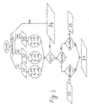
- analog image signals are input to an analog-digital converter 7 and a synchronization separator 8 via an input circuit.
- a reference horizontal synchronization signal Ref-HSynch is formed by the synchronization separator 8 via an interface filter 9 and is input to a PLL (phase locked loop) 10. From this and with knowledge of the number of pixels per line, the PLL 10 forms a pixel clock signal PixClk and a horizontal synchronization signal Hsync.
- the analog-digital converter 7 transmits a digital image signal RGB to an image processing device 14 and the green signal G thereof to an evaluation device 13.
- the horizontal synchronization signal Hsynch is fed to a detection device 12 for determining the start of a test line.
- the detection device 12 inputs a start signal Start to the evaluation device 13, which also records the pixel clock signal PixClk in addition to the green signal G.
- phase parameters ⁇ i are calculated, from which phase parameters ⁇ * i averaged over a plurality of rows are calculated in a subsequent filter 14, which are used in a subsequent signal phase determination device 15 for determining the phase position, this phase position in turn in a subsequent one Device for generating an A / D converter phase 16 is compared with a currently set phase position of the analog-digital converter, from which inter alia the horizontal shift signal HShft and a changed phase position of the analog-digital conversion is set.
- Further circuit components 17, 21, 22, 23 are used for precise readjustment and as an interface with a microprocessor.
- n measurement values are obtained from each pixel with corresponding phase positions.
- the basis of the method is that measured values of the same phase positions are subtracted from each other from white and black pixels and these differences are summed up over the entire test line to form phase parameters ⁇ i .
- the measurement values of adjacent pixels are advantageously subtracted from one another.
- phase position of the scanning can already be determined according to the invention from these phase parameters. This phase position is then optimized for the test line.
- the phase broadening of the HSync signal commonly referred to as jitter, continues to be problematic.
- This jitter is already counteracted by the PLL for regenerating the pixel clock signal, but since, on the other hand, the sampling time is to be adjusted to a fraction of a sampling period, it makes sense not only to use the current test line for calibration, but also to average over several lines , This averaging can include lines of the active image are carried out, whereby an optimized sampling time averaged over the active image is determined.
- a N-order FIR filter is particularly suitable for this purpose, the coefficients of which are all 1, ie
- a relatively low implementation effort can be achieved with IIR filters.
- the current phase position can now be determined mathematically from the ⁇ * i and the sampling phase of the A / D converter can be corrected accordingly.
- a comparison of the amounts of the averaged phase parameters first determines which of the two phase positions better matches the maxima and minima of the (green) image signal curve 1 of the measurement signal, which is assumed to be a sine curve.
- the larger phase parameter is taken as the better phase position.
- the better phase parameter is then compared with a limit value S and if the limit value is undershot in step 24, it is decided that there are no relevant sharp vertical lines or not enough lines of this type in the image and therefore there is no need for regulation.
- the phase position is selected as the best in steps 25, 26, the mean phase parameter of which is higher in amount.
- the sampling phase is further optimized by comparing the signs of the phase parameters and, if they match, the sampling phase in steps 28 and 31 (if the first sample is selected and the signs are the same or if the second sample is selected and the signs are unequal) by a predetermined value to the right and in the other cases in blocks 29 and 30 accordingly by a predetermined value to the left.
- the sign of the averaged phase parameters ⁇ * i is first determined and in the specified cases according to block 31 (if the signs of the first two samples are the same and different from the third sample), the first sample, according to block 32 (if all signs are the same) the second sample and according to block 33 (if the signs of the last two samples are the same and different from the first sample) the third sample is selected.
- block 34 recognizes that there is no relevant image with sharp vertical edges and that no change has been made. Then in the first three cases it is checked again whether the amount of the phase parameter of the best sampling
- the amounts of the (averaged) phase parameters of the subsequent sampling are
- a five-digit digital number with values between 0 and 31 can be used for the phase register.
- the phase register is increased or decreased by 1 according to the instruction above.
- the value 31 of the second scan is to be taken from the value 31 of the first scan with an increase by 1.
- the value 0 of the third scan is to be taken with an increase by 1.
- the setting device 11 for shifting the Hsync signal.
- the signal HShft causes the Hsync signal to be delayed by 0, 1 and 2 pixel clock cycles for all inputs; the start value after a reset is always 1. This results in a negative shift on the one hand and on the other hand causes the algorithm to deliver a result in the uncritical range for the next frame, since all samples will be shifted by a PixelClock cycle. This corresponds to a control range of the duration of a complete pixel.
- n 2: A / D-phase transition at 1st scan at 2nd scan 0 ⁇ 31 ⁇ 2nd scan ⁇ 1st scan HShift +1 HShift 0 31 ⁇ 0 ⁇ 2nd scan ⁇ 1st scan HShift 0 HShift -1
- n 3: A / D-phase transition 1st scan 2nd scan 3rd scan 0 ⁇ 31 ⁇ 3rd scan. ⁇ 1st scan. ⁇ 2nd scan. HShift +1 HShift 0 HShift 0 31 ⁇ 0 ⁇ 2nd scan. ⁇ 3rd scan. ⁇ 1st scan. HShift 0 HShift 0 0 HShift -1
Applications Claiming Priority (2)
| Application Number | Priority Date | Filing Date | Title |
|---|---|---|---|
| DE10136677 | 2001-07-27 | ||
| DE10136677A DE10136677A1 (de) | 2001-07-27 | 2001-07-27 | Verfahren und Anordnung zur Umwandlung analoger Bildsignale in digitale Bildsignale |
Publications (2)
| Publication Number | Publication Date |
|---|---|
| EP1280338A1 true EP1280338A1 (fr) | 2003-01-29 |
| EP1280338B1 EP1280338B1 (fr) | 2005-10-19 |
Family
ID=7693333
Family Applications (1)
| Application Number | Title | Priority Date | Filing Date |
|---|---|---|---|
| EP02016048A Expired - Lifetime EP1280338B1 (fr) | 2001-07-27 | 2002-07-19 | Méthode et système de conversion d' un signal d' image analogique en un signal d'image numérique basés sur la régulation de la phase du signal d' échantillonage |
Country Status (4)
| Country | Link |
|---|---|
| US (1) | US7183961B2 (fr) |
| EP (1) | EP1280338B1 (fr) |
| AT (1) | ATE307458T1 (fr) |
| DE (2) | DE10136677A1 (fr) |
Citations (3)
| Publication number | Priority date | Publication date | Assignee | Title |
|---|---|---|---|---|
| EP0756417A2 (fr) * | 1995-07-27 | 1997-01-29 | Hitachi, Ltd. | Dispositif de traitement de signal vidéo pour ajuster automatiquement la phase d'horloges d'échantillonnage |
| EP0918313A1 (fr) * | 1997-11-21 | 1999-05-26 | Deutsche Thomson-Brandt Gmbh | Méthode de traitement de signal pour un signal d'image analogique |
| US6097444A (en) * | 1998-09-11 | 2000-08-01 | Mitsubishi Denki Kabushiki Kaisha | Automatic image quality adjustment device adjusting phase of sampling clock for analog video signal to digital video signal conversion |
Family Cites Families (5)
| Publication number | Priority date | Publication date | Assignee | Title |
|---|---|---|---|---|
| IL82539A0 (en) * | 1987-05-15 | 1987-11-30 | Medaon Ltd | Video communication system and phase or frequency modulator included therein |
| GB2253103B (en) * | 1991-02-23 | 1994-08-31 | Motorola Inc | Video analog-to-digital converter |
| US5550594A (en) * | 1993-07-26 | 1996-08-27 | Pixel Instruments Corp. | Apparatus and method for synchronizing asynchronous signals |
| KR100258531B1 (ko) * | 1998-01-24 | 2000-06-15 | 윤종용 | 평판 디스플레이 장치의 화상 자동 조정 장치 및 방법 |
| US6490005B1 (en) * | 2000-06-30 | 2002-12-03 | Stmicroelectronics, Inc. | Video analog-to-digital converter |
-
2001
- 2001-07-27 DE DE10136677A patent/DE10136677A1/de not_active Ceased
-
2002
- 2002-07-19 EP EP02016048A patent/EP1280338B1/fr not_active Expired - Lifetime
- 2002-07-19 AT AT02016048T patent/ATE307458T1/de not_active IP Right Cessation
- 2002-07-19 DE DE50204575T patent/DE50204575D1/de not_active Expired - Lifetime
- 2002-07-25 US US10/205,589 patent/US7183961B2/en not_active Expired - Lifetime
Patent Citations (3)
| Publication number | Priority date | Publication date | Assignee | Title |
|---|---|---|---|---|
| EP0756417A2 (fr) * | 1995-07-27 | 1997-01-29 | Hitachi, Ltd. | Dispositif de traitement de signal vidéo pour ajuster automatiquement la phase d'horloges d'échantillonnage |
| EP0918313A1 (fr) * | 1997-11-21 | 1999-05-26 | Deutsche Thomson-Brandt Gmbh | Méthode de traitement de signal pour un signal d'image analogique |
| US6097444A (en) * | 1998-09-11 | 2000-08-01 | Mitsubishi Denki Kabushiki Kaisha | Automatic image quality adjustment device adjusting phase of sampling clock for analog video signal to digital video signal conversion |
Also Published As
| Publication number | Publication date |
|---|---|
| DE10136677A1 (de) | 2003-02-13 |
| US20030067559A1 (en) | 2003-04-10 |
| US7183961B2 (en) | 2007-02-27 |
| ATE307458T1 (de) | 2005-11-15 |
| EP1280338B1 (fr) | 2005-10-19 |
| DE50204575D1 (de) | 2005-11-24 |
Similar Documents
| Publication | Publication Date | Title |
|---|---|---|
| DE69733978T2 (de) | Bilddateninterpolationsgerät | |
| DE3609887C2 (de) | Schaltungsanordnung zur Erzeugung von Bemessungsfaktoren für ein rekursives Filter für Videosignale | |
| DE3021033C2 (de) | Verfahren zur bewegungskompensierten Zwischen-Halbbild-Kodierung | |
| DE3315109C2 (fr) | ||
| DE69726689T2 (de) | Wandlung eines Analogsignals, insbesondere eines Fernsehsignals, in einem Digitalsignal | |
| EP0567072B1 (fr) | Procédé et dispositif de détection de mode ciné | |
| DE3148129C2 (de) | Bildverarbeitungsgerät | |
| DE69933090T2 (de) | Signalverarbeitungsschaltung zur Rauschunterdrückung und Anzeigegerät | |
| DE3242734A1 (de) | Anordnung zum dynamischen einstellen einer schwarz/weiss-entscheidungsschwelle bei der bearbeitung von bildern mit graustufen | |
| DE2065353A1 (de) | Verfahren und vorrichtung zur korrektur der schattierungsverzerrung in einem bildsignal | |
| DE3304817C2 (de) | Verfahren und Vorrichtung zur automatischen Erkennung von Fehlern in Warenbahnen | |
| DE3538735C2 (fr) | ||
| EP1246452B1 (fr) | Méthode et dispositif de raidissement des transitions de signal dans des images de télévision | |
| DE3140825C2 (fr) | ||
| DE2655133C2 (de) | Verfahren zum Darstellen eines Videosignals auf dem Bildschirm eines Videosichtgerätes | |
| EP1280338A1 (fr) | Méthode et système de conversion d' un signal d' image analogique en un signal d'image numérique basés sur la régulation de la phase du signal d' échantillonage | |
| DE2720196A1 (de) | Diskriminierschaltung | |
| EP0017821B1 (fr) | Système et circuit pour l'exploitation d'images de télévision stationnaires, constituées par des lignes et des trames, en vue de la détection d'un changement de luminosité causé par le mouvement d'un objet | |
| DE10254469B4 (de) | Verfahren und Vorrichtung zur Bestimmung einer Frequenz für die Abtastung analoger Bilddaten | |
| DE3010559C2 (de) | Einrichtungen zur Feststellung von Fehlern in regelmäßigen Mustern | |
| EP0392977B1 (fr) | Circuit de compensation pour corriger les défauts d'image d'un système de projection d'image | |
| DE10331676A1 (de) | Verfahren zur Korrektur von Videosignalen | |
| EP0639922A2 (fr) | Circuit de détection de mouvement pour un signal d'image | |
| DE19913916C2 (de) | Verfahren und Einrichtung zum Ein- und/oder Nachstellen der Phase bei Flachbildschirmen | |
| DE3844876C2 (de) | Einrichtung zur automatischen Nachführung eines Meßbereichs |
Legal Events
| Date | Code | Title | Description |
|---|---|---|---|
| PUAI | Public reference made under article 153(3) epc to a published international application that has entered the european phase |
Free format text: ORIGINAL CODE: 0009012 |
|
| AK | Designated contracting states |
Designated state(s): AT BE BG CH CY CZ DE DK EE ES FI FR GB GR IE IT LI LU MC NL PT SE SK TR |
|
| AX | Request for extension of the european patent |
Extension state: AL LT LV MK RO SI |
|
| 17P | Request for examination filed |
Effective date: 20030628 |
|
| 17Q | First examination report despatched |
Effective date: 20030804 |
|
| AKX | Designation fees paid |
Designated state(s): AT BE BG CH CY CZ DE DK EE ES FI FR GB GR IE IT LI LU MC NL PT SE SK TR |
|
| GRAP | Despatch of communication of intention to grant a patent |
Free format text: ORIGINAL CODE: EPIDOSNIGR1 |
|
| GRAS | Grant fee paid |
Free format text: ORIGINAL CODE: EPIDOSNIGR3 |
|
| GRAA | (expected) grant |
Free format text: ORIGINAL CODE: 0009210 |
|
| AK | Designated contracting states |
Kind code of ref document: B1 Designated state(s): AT BE BG CH CY CZ DE DK EE ES FI FR GB GR IE IT LI LU MC NL PT SE SK TR |
|
| PG25 | Lapsed in a contracting state [announced via postgrant information from national office to epo] |
Ref country code: FI Free format text: LAPSE BECAUSE OF FAILURE TO SUBMIT A TRANSLATION OF THE DESCRIPTION OR TO PAY THE FEE WITHIN THE PRESCRIBED TIME-LIMIT Effective date: 20051019 Ref country code: NL Free format text: LAPSE BECAUSE OF FAILURE TO SUBMIT A TRANSLATION OF THE DESCRIPTION OR TO PAY THE FEE WITHIN THE PRESCRIBED TIME-LIMIT Effective date: 20051019 Ref country code: IE Free format text: LAPSE BECAUSE OF FAILURE TO SUBMIT A TRANSLATION OF THE DESCRIPTION OR TO PAY THE FEE WITHIN THE PRESCRIBED TIME-LIMIT Effective date: 20051019 Ref country code: SK Free format text: LAPSE BECAUSE OF FAILURE TO SUBMIT A TRANSLATION OF THE DESCRIPTION OR TO PAY THE FEE WITHIN THE PRESCRIBED TIME-LIMIT Effective date: 20051019 Ref country code: CZ Free format text: LAPSE BECAUSE OF FAILURE TO SUBMIT A TRANSLATION OF THE DESCRIPTION OR TO PAY THE FEE WITHIN THE PRESCRIBED TIME-LIMIT Effective date: 20051019 |
|
| REG | Reference to a national code |
Ref country code: GB Ref legal event code: FG4D Free format text: NOT ENGLISH |
|
| REG | Reference to a national code |
Ref country code: CH Ref legal event code: EP |
|
| REG | Reference to a national code |
Ref country code: IE Ref legal event code: FG4D Free format text: LANGUAGE OF EP DOCUMENT: GERMAN |
|
| REF | Corresponds to: |
Ref document number: 50204575 Country of ref document: DE Date of ref document: 20051124 Kind code of ref document: P |
|
| PG25 | Lapsed in a contracting state [announced via postgrant information from national office to epo] |
Ref country code: SE Free format text: LAPSE BECAUSE OF FAILURE TO SUBMIT A TRANSLATION OF THE DESCRIPTION OR TO PAY THE FEE WITHIN THE PRESCRIBED TIME-LIMIT Effective date: 20060119 Ref country code: BG Free format text: LAPSE BECAUSE OF FAILURE TO SUBMIT A TRANSLATION OF THE DESCRIPTION OR TO PAY THE FEE WITHIN THE PRESCRIBED TIME-LIMIT Effective date: 20060119 Ref country code: GR Free format text: LAPSE BECAUSE OF FAILURE TO SUBMIT A TRANSLATION OF THE DESCRIPTION OR TO PAY THE FEE WITHIN THE PRESCRIBED TIME-LIMIT Effective date: 20060119 Ref country code: DK Free format text: LAPSE BECAUSE OF FAILURE TO SUBMIT A TRANSLATION OF THE DESCRIPTION OR TO PAY THE FEE WITHIN THE PRESCRIBED TIME-LIMIT Effective date: 20060119 |
|
| PG25 | Lapsed in a contracting state [announced via postgrant information from national office to epo] |
Ref country code: ES Free format text: LAPSE BECAUSE OF FAILURE TO SUBMIT A TRANSLATION OF THE DESCRIPTION OR TO PAY THE FEE WITHIN THE PRESCRIBED TIME-LIMIT Effective date: 20060130 |
|
| GBT | Gb: translation of ep patent filed (gb section 77(6)(a)/1977) |
Effective date: 20060123 |
|
| PG25 | Lapsed in a contracting state [announced via postgrant information from national office to epo] |
Ref country code: PT Free format text: LAPSE BECAUSE OF FAILURE TO SUBMIT A TRANSLATION OF THE DESCRIPTION OR TO PAY THE FEE WITHIN THE PRESCRIBED TIME-LIMIT Effective date: 20060320 |
|
| NLV1 | Nl: lapsed or annulled due to failure to fulfill the requirements of art. 29p and 29m of the patents act | ||
| REG | Reference to a national code |
Ref country code: IE Ref legal event code: FD4D |
|
| ET | Fr: translation filed | ||
| PGFP | Annual fee paid to national office [announced via postgrant information from national office to epo] |
Ref country code: MC Payment date: 20060704 Year of fee payment: 5 |
|
| PGFP | Annual fee paid to national office [announced via postgrant information from national office to epo] |
Ref country code: AT Payment date: 20060705 Year of fee payment: 5 |
|
| PGFP | Annual fee paid to national office [announced via postgrant information from national office to epo] |
Ref country code: CH Payment date: 20060727 Year of fee payment: 5 |
|
| PGFP | Annual fee paid to national office [announced via postgrant information from national office to epo] |
Ref country code: LU Payment date: 20060804 Year of fee payment: 5 |
|
| PLBE | No opposition filed within time limit |
Free format text: ORIGINAL CODE: 0009261 |
|
| STAA | Information on the status of an ep patent application or granted ep patent |
Free format text: STATUS: NO OPPOSITION FILED WITHIN TIME LIMIT |
|
| PGFP | Annual fee paid to national office [announced via postgrant information from national office to epo] |
Ref country code: BE Payment date: 20060828 Year of fee payment: 5 |
|
| 26N | No opposition filed |
Effective date: 20060720 |
|
| BERE | Be: lapsed |
Owner name: HARMAN/BECKER AUTOMOTIVE SYSTEMS (XSYS DIVISION) Effective date: 20070731 |
|
| REG | Reference to a national code |
Ref country code: CH Ref legal event code: PL |
|
| PG25 | Lapsed in a contracting state [announced via postgrant information from national office to epo] |
Ref country code: CH Free format text: LAPSE BECAUSE OF NON-PAYMENT OF DUE FEES Effective date: 20070731 Ref country code: LI Free format text: LAPSE BECAUSE OF NON-PAYMENT OF DUE FEES Effective date: 20070731 Ref country code: MC Free format text: LAPSE BECAUSE OF NON-PAYMENT OF DUE FEES Effective date: 20070731 |
|
| PG25 | Lapsed in a contracting state [announced via postgrant information from national office to epo] |
Ref country code: AT Free format text: LAPSE BECAUSE OF NON-PAYMENT OF DUE FEES Effective date: 20070719 Ref country code: EE Free format text: LAPSE BECAUSE OF FAILURE TO SUBMIT A TRANSLATION OF THE DESCRIPTION OR TO PAY THE FEE WITHIN THE PRESCRIBED TIME-LIMIT Effective date: 20051019 |
|
| PG25 | Lapsed in a contracting state [announced via postgrant information from national office to epo] |
Ref country code: TR Free format text: LAPSE BECAUSE OF FAILURE TO SUBMIT A TRANSLATION OF THE DESCRIPTION OR TO PAY THE FEE WITHIN THE PRESCRIBED TIME-LIMIT Effective date: 20051019 |
|
| PG25 | Lapsed in a contracting state [announced via postgrant information from national office to epo] |
Ref country code: BE Free format text: LAPSE BECAUSE OF NON-PAYMENT OF DUE FEES Effective date: 20070731 |
|
| PG25 | Lapsed in a contracting state [announced via postgrant information from national office to epo] |
Ref country code: CY Free format text: LAPSE BECAUSE OF FAILURE TO SUBMIT A TRANSLATION OF THE DESCRIPTION OR TO PAY THE FEE WITHIN THE PRESCRIBED TIME-LIMIT Effective date: 20051019 |
|
| PG25 | Lapsed in a contracting state [announced via postgrant information from national office to epo] |
Ref country code: LU Free format text: LAPSE BECAUSE OF NON-PAYMENT OF DUE FEES Effective date: 20070719 |
|
| REG | Reference to a national code |
Ref country code: FR Ref legal event code: PLFP Year of fee payment: 15 |
|
| REG | Reference to a national code |
Ref country code: FR Ref legal event code: PLFP Year of fee payment: 16 |
|
| REG | Reference to a national code |
Ref country code: FR Ref legal event code: PLFP Year of fee payment: 17 |
|
| PGFP | Annual fee paid to national office [announced via postgrant information from national office to epo] |
Ref country code: FR Payment date: 20180621 Year of fee payment: 17 Ref country code: IT Payment date: 20180620 Year of fee payment: 17 |
|
| PGFP | Annual fee paid to national office [announced via postgrant information from national office to epo] |
Ref country code: DE Payment date: 20180620 Year of fee payment: 17 Ref country code: GB Payment date: 20180621 Year of fee payment: 17 |
|
| REG | Reference to a national code |
Ref country code: DE Ref legal event code: R119 Ref document number: 50204575 Country of ref document: DE |
|
| GBPC | Gb: european patent ceased through non-payment of renewal fee |
Effective date: 20190719 |
|
| PG25 | Lapsed in a contracting state [announced via postgrant information from national office to epo] |
Ref country code: GB Free format text: LAPSE BECAUSE OF NON-PAYMENT OF DUE FEES Effective date: 20190719 Ref country code: DE Free format text: LAPSE BECAUSE OF NON-PAYMENT OF DUE FEES Effective date: 20200201 |
|
| PG25 | Lapsed in a contracting state [announced via postgrant information from national office to epo] |
Ref country code: FR Free format text: LAPSE BECAUSE OF NON-PAYMENT OF DUE FEES Effective date: 20190731 |
|
| PG25 | Lapsed in a contracting state [announced via postgrant information from national office to epo] |
Ref country code: IT Free format text: LAPSE BECAUSE OF NON-PAYMENT OF DUE FEES Effective date: 20190719 |