EP1280338A1 - Method and arrangement for converting analog picture signals in digital picture signals by adjusting the phase of the sampling signal - Google Patents
Method and arrangement for converting analog picture signals in digital picture signals by adjusting the phase of the sampling signal Download PDFInfo
- Publication number
- EP1280338A1 EP1280338A1 EP02016048A EP02016048A EP1280338A1 EP 1280338 A1 EP1280338 A1 EP 1280338A1 EP 02016048 A EP02016048 A EP 02016048A EP 02016048 A EP02016048 A EP 02016048A EP 1280338 A1 EP1280338 A1 EP 1280338A1
- Authority
- EP
- European Patent Office
- Prior art keywords
- phase
- parameters
- phase position
- signal
- image signals
- Prior art date
- Legal status (The legal status is an assumption and is not a legal conclusion. Google has not performed a legal analysis and makes no representation as to the accuracy of the status listed.)
- Granted
Links
Images


Classifications
-
- G—PHYSICS
- G09—EDUCATION; CRYPTOGRAPHY; DISPLAY; ADVERTISING; SEALS
- G09G—ARRANGEMENTS OR CIRCUITS FOR CONTROL OF INDICATING DEVICES USING STATIC MEANS TO PRESENT VARIABLE INFORMATION
- G09G5/00—Control arrangements or circuits for visual indicators common to cathode-ray tube indicators and other visual indicators
- G09G5/003—Details of a display terminal, the details relating to the control arrangement of the display terminal and to the interfaces thereto
- G09G5/006—Details of the interface to the display terminal
- G09G5/008—Clock recovery
-
- H—ELECTRICITY
- H04—ELECTRIC COMMUNICATION TECHNIQUE
- H04N—PICTORIAL COMMUNICATION, e.g. TELEVISION
- H04N5/00—Details of television systems
- H04N5/04—Synchronising
- H04N5/12—Devices in which the synchronising signals are only operative if a phase difference occurs between synchronising and synchronised scanning devices, e.g. flywheel synchronising
- H04N5/126—Devices in which the synchronising signals are only operative if a phase difference occurs between synchronising and synchronised scanning devices, e.g. flywheel synchronising whereby the synchronisation signal indirectly commands a frequency generator
-
- H—ELECTRICITY
- H04—ELECTRIC COMMUNICATION TECHNIQUE
- H04N—PICTORIAL COMMUNICATION, e.g. TELEVISION
- H04N5/00—Details of television systems
- H04N5/14—Picture signal circuitry for video frequency region
-
- G—PHYSICS
- G09—EDUCATION; CRYPTOGRAPHY; DISPLAY; ADVERTISING; SEALS
- G09G—ARRANGEMENTS OR CIRCUITS FOR CONTROL OF INDICATING DEVICES USING STATIC MEANS TO PRESENT VARIABLE INFORMATION
- G09G3/00—Control arrangements or circuits, of interest only in connection with visual indicators other than cathode-ray tubes
- G09G3/20—Control arrangements or circuits, of interest only in connection with visual indicators other than cathode-ray tubes for presentation of an assembly of a number of characters, e.g. a page, by composing the assembly by combination of individual elements arranged in a matrix no fixed position being assigned to or needed to be assigned to the individual characters or partial characters
- G09G3/2092—Details of a display terminals using a flat panel, the details relating to the control arrangement of the display terminal and to the interfaces thereto
Definitions
- the invention relates to a method and an arrangement for converting analog image signals into digital image signals.
- the selection of the sampling phase is not without problems. Errors in the selection of the scanning phase are most evident in images with sharp vertical edges, such as those for navigation maps etc. occur.
- the scanning of a test line with alternating black and white pixels can thus be used to assess a selected phase position. If - in extreme cases - the phase position lies exactly between the minima and maxima, a uniformly periodic test line - e.g. a sine curve - matching gray tones are determined and the test line is therefore displayed as a gray line.
- the synchronization signals which determine the time of sampling, are modulated onto the actual RGB signal in order to minimize runtime differences between image content and control signals.
- the lines generated by the source are generated with a precisely defined number of pixels, so that the reception module is able to determine the exact number by correspondingly multiplying the line frequency Regenerate pixel frequency.
- a defined test signal is punched in by the source, which preferably switches the maximum and minimum RGB amplitude from one pixel to the next - that is, an alternating sequence of white and black pixels. includes.
- the sampling frequency is generated by a phase locked loop (PLL) based on the knowledge of the exact number of pixels per line and a corresponding multiplication of the line frequency, the optimum sampling phase must still be determined from the sampling signal.
- PLL phase locked loop
- the invention is accordingly based on the object of providing a method and an arrangement for converting analog image signals into digital image signals with which an exact determination of the phase position between the recovered synchronization signal and RGB signal is advantageously possible with relatively little effort.
- the invention is based on the idea of determining the actual phase position of the RGB signal by means of a finer sampling with different phase positions and a qualitative evaluation of the measured values by forming suitable parameters.
- the pixels of a test line are preferably scanned with alternating white and black pixels at a frequency that is n times the pixel frequency.
- n samples with fixed phase positions are obtained for each pixel.
- the parameters for the individual phase positions are determined by forming the difference between the measured values of adjacent pixels and summing up these differences. These parameters therefore contain Information on the relative phase position between the recovered synchronization signal and the RGB signal, which can be evaluated below.
- test line is advantageously used for calibration, but several lines. This can be done in particular by low-pass filtering.
- readjustment of the sampling time can be omitted if it is recognized that there is no image with relevant vertical sharp lines and the problems mentioned at the outset are therefore not relevant.
- the method according to the invention can in particular be carried out with double or triple oversampling.
- Each pixel is hereby divided into 2 or 3 phase areas, each of which is described by a phase register, with the phase register value of the sampling phase being increased or decreased step-by-step in the case of readjustment.
- analog image signals are input to an analog-digital converter 7 and a synchronization separator 8 via an input circuit.
- a reference horizontal synchronization signal Ref-HSynch is formed by the synchronization separator 8 via an interface filter 9 and is input to a PLL (phase locked loop) 10. From this and with knowledge of the number of pixels per line, the PLL 10 forms a pixel clock signal PixClk and a horizontal synchronization signal Hsync.
- the analog-digital converter 7 transmits a digital image signal RGB to an image processing device 14 and the green signal G thereof to an evaluation device 13.
- the horizontal synchronization signal Hsynch is fed to a detection device 12 for determining the start of a test line.
- the detection device 12 inputs a start signal Start to the evaluation device 13, which also records the pixel clock signal PixClk in addition to the green signal G.
- phase parameters ⁇ i are calculated, from which phase parameters ⁇ * i averaged over a plurality of rows are calculated in a subsequent filter 14, which are used in a subsequent signal phase determination device 15 for determining the phase position, this phase position in turn in a subsequent one Device for generating an A / D converter phase 16 is compared with a currently set phase position of the analog-digital converter, from which inter alia the horizontal shift signal HShft and a changed phase position of the analog-digital conversion is set.
- Further circuit components 17, 21, 22, 23 are used for precise readjustment and as an interface with a microprocessor.
- n measurement values are obtained from each pixel with corresponding phase positions.
- the basis of the method is that measured values of the same phase positions are subtracted from each other from white and black pixels and these differences are summed up over the entire test line to form phase parameters ⁇ i .
- the measurement values of adjacent pixels are advantageously subtracted from one another.
- phase position of the scanning can already be determined according to the invention from these phase parameters. This phase position is then optimized for the test line.
- the phase broadening of the HSync signal commonly referred to as jitter, continues to be problematic.
- This jitter is already counteracted by the PLL for regenerating the pixel clock signal, but since, on the other hand, the sampling time is to be adjusted to a fraction of a sampling period, it makes sense not only to use the current test line for calibration, but also to average over several lines , This averaging can include lines of the active image are carried out, whereby an optimized sampling time averaged over the active image is determined.
- a N-order FIR filter is particularly suitable for this purpose, the coefficients of which are all 1, ie
- a relatively low implementation effort can be achieved with IIR filters.
- the current phase position can now be determined mathematically from the ⁇ * i and the sampling phase of the A / D converter can be corrected accordingly.
- a comparison of the amounts of the averaged phase parameters first determines which of the two phase positions better matches the maxima and minima of the (green) image signal curve 1 of the measurement signal, which is assumed to be a sine curve.
- the larger phase parameter is taken as the better phase position.
- the better phase parameter is then compared with a limit value S and if the limit value is undershot in step 24, it is decided that there are no relevant sharp vertical lines or not enough lines of this type in the image and therefore there is no need for regulation.
- the phase position is selected as the best in steps 25, 26, the mean phase parameter of which is higher in amount.
- the sampling phase is further optimized by comparing the signs of the phase parameters and, if they match, the sampling phase in steps 28 and 31 (if the first sample is selected and the signs are the same or if the second sample is selected and the signs are unequal) by a predetermined value to the right and in the other cases in blocks 29 and 30 accordingly by a predetermined value to the left.
- the sign of the averaged phase parameters ⁇ * i is first determined and in the specified cases according to block 31 (if the signs of the first two samples are the same and different from the third sample), the first sample, according to block 32 (if all signs are the same) the second sample and according to block 33 (if the signs of the last two samples are the same and different from the first sample) the third sample is selected.
- block 34 recognizes that there is no relevant image with sharp vertical edges and that no change has been made. Then in the first three cases it is checked again whether the amount of the phase parameter of the best sampling
- the amounts of the (averaged) phase parameters of the subsequent sampling are
- a five-digit digital number with values between 0 and 31 can be used for the phase register.
- the phase register is increased or decreased by 1 according to the instruction above.
- the value 31 of the second scan is to be taken from the value 31 of the first scan with an increase by 1.
- the value 0 of the third scan is to be taken with an increase by 1.
- the setting device 11 for shifting the Hsync signal.
- the signal HShft causes the Hsync signal to be delayed by 0, 1 and 2 pixel clock cycles for all inputs; the start value after a reset is always 1. This results in a negative shift on the one hand and on the other hand causes the algorithm to deliver a result in the uncritical range for the next frame, since all samples will be shifted by a PixelClock cycle. This corresponds to a control range of the duration of a complete pixel.
- n 2: A / D-phase transition at 1st scan at 2nd scan 0 ⁇ 31 ⁇ 2nd scan ⁇ 1st scan HShift +1 HShift 0 31 ⁇ 0 ⁇ 2nd scan ⁇ 1st scan HShift 0 HShift -1
- n 3: A / D-phase transition 1st scan 2nd scan 3rd scan 0 ⁇ 31 ⁇ 3rd scan. ⁇ 1st scan. ⁇ 2nd scan. HShift +1 HShift 0 HShift 0 31 ⁇ 0 ⁇ 2nd scan. ⁇ 3rd scan. ⁇ 1st scan. HShift 0 HShift 0 0 HShift -1
Landscapes
- Engineering & Computer Science (AREA)
- Multimedia (AREA)
- Signal Processing (AREA)
- General Physics & Mathematics (AREA)
- Theoretical Computer Science (AREA)
- Physics & Mathematics (AREA)
- Computer Hardware Design (AREA)
- Control Of Indicators Other Than Cathode Ray Tubes (AREA)
- Television Systems (AREA)
- Picture Signal Circuits (AREA)
- Facsimile Scanning Arrangements (AREA)
- Color Television Image Signal Generators (AREA)
- Liquid Crystal Display Device Control (AREA)
- Analogue/Digital Conversion (AREA)
- Color Television Systems (AREA)
Abstract
Description
Die Erfindung bezieht sich auf ein Verfahren und eine Anordnung zur Umwandlung analoger Bildsignale in digitale Bildsignale.The invention relates to a method and an arrangement for converting analog image signals into digital image signals.
Zur Darstellung eines analogen RGB-Bildes auf einem digitalen Display ist eine Analog-Digital-Wandlung erforderlich. Hierbei ist die Qualität der Bilddarstellung wesentlich davon abhängig, dass diese Wandlung pixelgenau erfolgt. Anderenfalls werden feine senkrechte Linienstrukturen nur unzureichend wiedergegeben. Falls die Abtastfrequenz nicht der Pixelfrequenz entspricht, können durch Abtastung außerhalb der minimalen und maximalen Bildsignalwerte falsche Minima und Maxima erkannt werden, die weder in ihrem Betrag noch in ihrer Phase mit den tatsächlichen Werten übereinstimmen.To display an analog RGB image on a digital display, an analog-to-digital conversion is required. The quality of the image is largely dependent on the fact that this conversion takes place with pixel accuracy. Otherwise, fine vertical line structures are not reproduced adequately. If the sampling frequency does not correspond to the pixel frequency, false minima and maxima can be recognized by sampling outside the minimum and maximum image signal values, the minima and phase of which do not match the actual values.
Aber auch in dem Fall, dass die Abtastfrequenz der Pixelfrequenz entspricht, ist die Wahl der Abtastphase nicht unproblematisch. Fehler in der Wahl der Abtastphase zeigen sich am deutlichsten bei Bildern mit scharfen vertikalen Kanten, wie sie z.B. bei Navigationskarten u.s.w. auftreten. Die Abtastung einer Testzeile mit alternierenden schwarzen und weißen Pixeln kann somit zur Beurteilung einer gewählten Phasenlage herangezogen werden. Falls - im Extremfall - die Phasenlage genau zwischen den Minima und Maxima liegt, werden bei einer gleichmäßig periodischen Testzeile - z.B. einer Sinuskurve - übereinstimmende Grautöne ermittelt und somit die Testzeile als graue Zeile wiedergegeben.But even in the event that the sampling frequency corresponds to the pixel frequency, the selection of the sampling phase is not without problems. Errors in the selection of the scanning phase are most evident in images with sharp vertical edges, such as those for navigation maps etc. occur. The scanning of a test line with alternating black and white pixels can thus be used to assess a selected phase position. If - in extreme cases - the phase position lies exactly between the minima and maxima, a uniformly periodic test line - e.g. a sine curve - matching gray tones are determined and the test line is therefore displayed as a gray line.
Um derartige Probleme gering zu halten, werden zum einen die Synchronisationssignale, die den Zeitpunkt der Abtastung bestimmen, dem eigentlichen RGB-Signal aufmoduliert, um Laufzeitunterschiede zwischen Bildinhalt und Steuersignalen zu minimieren. Weiterhin werden die von der Quelle erzeugten Zeilen mit einer genau definierten Anzahl an Pixeln generiert, so dass es dem Empfangsmodul möglich ist, durch entsprechende Vervielfachung der Zeilenfrequenz die genaue Pixelfrequenz zu regenerieren. Zur Auswahl der Phasenlage zwischen rückgewonnenem Synchronisationssignal und RGB-Signal durch das Empfangsmodul wird von der Quelle ein definiertes Testsignal eingestanzt, das vorzugsweise einen Wechsel zwischen maximaler und minimaler RGB-Amplitude von einem Pixel zum nächsten - d.h. eine alternierende Folge von weißen und schwarzen Pixeln - beinhaltet.In order to keep such problems to a minimum, the synchronization signals, which determine the time of sampling, are modulated onto the actual RGB signal in order to minimize runtime differences between image content and control signals. Furthermore, the lines generated by the source are generated with a precisely defined number of pixels, so that the reception module is able to determine the exact number by correspondingly multiplying the line frequency Regenerate pixel frequency. To select the phase position between the recovered synchronization signal and the RGB signal by the receiving module, a defined test signal is punched in by the source, which preferably switches the maximum and minimum RGB amplitude from one pixel to the next - that is, an alternating sequence of white and black pixels. includes.
Da die Abtastfrequenz aufgrund der Kenntnis der exakten Pixelanzahl pro Zeile und einer entsprechenden Vervielfachung der Zeilenfrequenz durch einen phasengerasteten Regelkreis (PLL) erzeugt wird, muss aus dem Abtastsignal noch die optimale Abtastphase zu bestimmt werden.Since the sampling frequency is generated by a phase locked loop (PLL) based on the knowledge of the exact number of pixels per line and a corresponding multiplication of the line frequency, the optimum sampling phase must still be determined from the sampling signal.
Der Erfindung liegt dementsprechend die Aufgabe zugrunde, ein Verfahren und eine Anordnung zur Umwandlung analoger Bildsignale in digitale Bildsignale zu schaffen, mit denen eine genaue Ermittlung der Phasenlage zwischen rückgewonnenem Synchronisationssignal und RGB-Signal mit vorteilhafterweise relativ geringem Aufwand möglich ist.The invention is accordingly based on the object of providing a method and an arrangement for converting analog image signals into digital image signals with which an exact determination of the phase position between the recovered synchronization signal and RGB signal is advantageously possible with relatively little effort.
Diese Aufgabe wird durch ein Verfahren nach Anspruch 1 und eine Anordnung nach Anspruch 13 gelöst. Die Unteransprüche beschreiben bevorzugte Weiterbildungen.This object is achieved by a method according to
Der Erfindung liegt der Gedanke zugrunde, die tatsächliche Phasenlage des RGB-Signals durch eine feinere Abtastung mit unterschiedlichen Phasenlagen und eine qualitative Auswertung der Messwerte durch Bildung geeigneter Parameter zu ermitteln. Hierzu wird eine Abtastung der Pixel einer Testzeile mit vorzugsweise alternierend weißen und schwarzen Pixeln mit einer Frequenz vorgenommen, die ein n-faches der Pixelfrequenz ist. Hierdurch werden zu jedem Pixel n Abtastwerte mit festen Phasenlagen gewonnen. Die Ermittlung der Parameter zu den einzelnen Phasenlagen erfolgt durch Differenzbildung der Messwerte benachbarter Pixel und Summation dieser Differenzen. Diese Parameter enthalten somit Informationen zu der relativen Phasenlage zwischen rückgewonnenem Synchronisationssignal und RGB-Signal, die nachfolgend ausgewertet werden können.The invention is based on the idea of determining the actual phase position of the RGB signal by means of a finer sampling with different phase positions and a qualitative evaluation of the measured values by forming suitable parameters. For this purpose, the pixels of a test line are preferably scanned with alternating white and black pixels at a frequency that is n times the pixel frequency. As a result, n samples with fixed phase positions are obtained for each pixel. The parameters for the individual phase positions are determined by forming the difference between the measured values of adjacent pixels and summing up these differences. These parameters therefore contain Information on the relative phase position between the recovered synchronization signal and the RGB signal, which can be evaluated below.
Um einem Hsync-Jitter, d.h. einer Phasenschwankung des Hsynch-Signals, entgegenzuwirken und dennoch den Abtastzeitpunkt auf den Bruchteil einer Abtastperiode genau zu ermitteln, wird vorteilhafterweise nicht nur die Testzeile zur Kalibrierung verwendet, sondern mehrere Zeilen. Dies kann insbesondere durch eine Tiefpassfilterung erfolgen.To an Hsync jitter, i.e. To counteract a phase fluctuation of the Hsynch signal and yet to determine the sampling instant precisely to a fraction of a sampling period, not only the test line is advantageously used for calibration, but several lines. This can be done in particular by low-pass filtering.
Erfindungsgemäß kann eine Nachregelung des Abtastzeitpunktes unterbleiben, wenn erkannt wird, das kein Bild mit relevanten vertikalen scharfen Linien vorliegt und somit die eingangs genannten Probleme nicht relevant sind.According to the invention, readjustment of the sampling time can be omitted if it is recognized that there is no image with relevant vertical sharp lines and the problems mentioned at the outset are therefore not relevant.
Das erfindungsgemäße Verfahren kann insbesondere mit 2-facher oder 3-facher Überabtastung durchgeführt werden. Jedes Pixel wird hierdurch in 2 oder 3 Phasenbereiche unterteilt, die jeweils durch ein Phasenregister beschrieben werden, wobei bei einer Nachregelung entsprechend der Phasenregisterwert der Abtastphase schrittweise erhöht oder verringert wird.The method according to the invention can in particular be carried out with double or triple oversampling. Each pixel is hereby divided into 2 or 3 phase areas, each of which is described by a phase register, with the phase register value of the sampling phase being increased or decreased step-by-step in the case of readjustment.
Die Erfindung wird im folgenden anhand der beiliegenden Zeichnungen an einigen Ausführungsformen näher erläutert. Es zeigen:
Figur 1 ein Zeitdiagramm eines Messsignals gemäß einer ersten Ausführungsform der Erfindung mit 2-facher Überabtastung;Figur 2 ein Zeitdiagramm eines Messsignals gemäß einer weiteren Ausführungsform der Erfindung mit 3-facher Überabtastung;Figur 3 den Aufbau einer erfindungsgemäßen Anordnung zur Durchführung des erfindungsgemäßen Verfahrens;- Figur 4 ein Flussdiagramm eines erfindungsgemäßen Verfahrens gemäß einer Ausführungsform der Erfindung;
Figur 5 ein Flussdiagramm eines erfindungsgemäßen Verfahrens gemäß einer weiteren Ausführungsform der Erfindung.
- Figure 1 is a timing diagram of a measurement signal according to a first embodiment of the invention with double oversampling;
- FIG. 2 shows a time diagram of a measurement signal according to a further embodiment of the invention with triple oversampling;
- Figure 3 shows the structure of an arrangement according to the invention for performing the method according to the invention;
- FIG. 4 shows a flow diagram of a method according to the invention in accordance with an embodiment of the invention;
- FIG. 5 shows a flow diagram of a method according to the invention in accordance with a further embodiment of the invention.
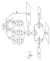
Gemäß Figur 3 werden analoge Bildsignale über eine Eingangsschaltung einem Analog-Digital-Wandler 7 sowie einem Synchronisationsseparator 8 eingegeben. Von dem Synchronisationsseparator 8 wird über ein Schnittstellen-Filter 9 ein Referenz-Horizontal-Synchronisationssignal Ref-HSynch gebildet, das einem PLL (phasengerasteten Regelkreis) 10 eingegeben wird. Der PLL 10 bildet hieraus und mit Kenntnis der Pixelzahl pro Zeile ein Pixel-Taktsignal PixClk und ein Horizontalsynchronisationssignal Hsync. Der Analog-Digital-Wandler 7 gibt ein digitales Bildsignal RGB an eine Bildbearbeitungseinrichtung 14 und das Grünsignal G hiervon an eine Auswerteeinrichtung 13 weiter. Über eine Einstelleinrichtung 11 zum Verschieben des Horizontal-Synchronisationssignals Hsynch in Abhängigkeit von einem Horizontal-Verschiebesignal HShft wird das Horizontal-Synchronisationssignal Hsynch einer Detektionseinrichtung 12 zur Feststellung eines Beginns einer Testzeile zugeführt. Die Detektionseinrichtung 12 gibt ein Startsignal Start an die Auswerteeinrichtung 13 ein, die weiterhin neben dem Grün-Signal G das Pixel-Taktsignal PixClk aufnimmt. In der Auswerteeinrichtung 13 werden Phasenparameter θi berechnet, aus denen in einem nachfolgenden Filter 14 durch eine Mittelung über mehrere Zeilen gemittelte Phasenparameter θ*i berechnet werden, die in einer nachfolgenden Signalphasenbestimmungseinrichtung 15 zur Bestimmung der Phasenlage herangezogen werden, wobei diese Phasenlage wiederum in einer nachfolgenden Einrichtung zum Erzeugen einer A/D-Wandler-Phase 16 mit einer derzeit eingestellten Phasenlage des Analog-Digital-Wandlers verglichen wird, woraus unter anderem das Horizontal-Verschiebesignal HShft und eine geänderte Phasenlage der Analog-Digital-Wandlung festgelegt wird. Weitere Schaltungskomponenten 17, 21, 22, 23 dienen der genauen Nachregelung und als Schnittstelle mit einem Mikroprozessor.According to FIG. 3, analog image signals are input to an analog-
In der Auswerteeinrichtung 13 werden die Zeilen der digitalen Grün-Bildsignale G mit einer n-fachen Pixelfrequenz ausgelesen. Aus einer Testzeile, die vorzugsweise die letzte Zeile vor dem aktiven Bild ist und alternierend weiße und schwarze Pixel aufweist, werden pro Pixel n Messwerte abgetastet. In Figur 1 ist hierzu ein Beispiel mit n=2 und in Figur 2 ein Beispiel mit n=3 gezeigt. In der Detektionseinrichtung 12 wird hierbei der Anfang der Testzeile festgestellt und ein Startsignal Start an die Auswerteeinheit ausgeben.In the
Durch die Vielfachabtastung werden von jedem Pixel n Messwerte bei jeweils sich entsprechenden Phasenlagen gewonnen. Grundlage des Verfahrens ist es, dass jeweils Messwerte gleicher Phasenlagen von weißen und schwarzen Pixeln voneinander subtrahiert werden und diese Differenzen über die gesamte Testzeile zu Phasenparametern θi aufsummiert werden. Vorteilhafterweise werden hierzu die Messwerte benachbarter Pixel voneinander subtrahiert.Due to the multiple scanning, n measurement values are obtained from each pixel with corresponding phase positions. The basis of the method is that measured values of the same phase positions are subtracted from each other from white and black pixels and these differences are summed up over the entire test line to form phase parameters θ i . For this purpose, the measurement values of adjacent pixels are advantageously subtracted from one another.
Grundsätzlich kann erfindungsgemäß bereits aus diesen Phasenparametern die Phasenlage der Abtastung bestimmt werden. Dese Phasenlage ist dann für die Testzeile optimiert. Problematisch ist jedoch weiterhin die allgemein als Jitter bezeichnete Phasenverbreiterung des HSync-Signals. Zwar wird durch die PLL zur Regenerierung des Pixel-Taktsignals diesem Jitter bereits entgegengewirkt, da jedoch andererseits der Abtastzeitpunkt auf den Bruchteil einer Abtastperiode abgeglichen werden soll, ist es sinnvoll, nicht nur die aktuelle Testzeile zur Kalibrierung zu verwenden, sondern über mehrere Zeilen zu mitteln. Diese Mittelung kann insbesondere unter Einbeziehung von Zeilen des aktiven Bildes vorgenommen werden, wodurch ein über das aktive Bild gemittelter otimierter Abtastzeitpunkt bestimmt wird.In principle, the phase position of the scanning can already be determined according to the invention from these phase parameters. This phase position is then optimized for the test line. However, the phase broadening of the HSync signal, commonly referred to as jitter, continues to be problematic. This jitter is already counteracted by the PLL for regenerating the pixel clock signal, but since, on the other hand, the sampling time is to be adjusted to a fraction of a sampling period, it makes sense not only to use the current test line for calibration, but also to average over several lines , This averaging can include lines of the active image are carried out, whereby an optimized sampling time averaged over the active image is determined.
Diese Mittelung erfolgt durch Tiefpassfilterung. Hierzu eignet sich insbesondere ein FIR-Filter N-ter Ordnung, dessen Koeffizienten alle 1 sind, d.h.
Dieses Filter kann auch z.B. mit N=15 implementiert werden. Ein relativ geringer Realisierungsaufwand kann durch IIR-Filter erreicht werden. Hierbei kann insbesondere eine Realisierung gewählt werden mit der Form
Aus den θ*i kann nun mathematisch die aktuelle Phasenlage ermittelt und entsprechend die Abtastphase des A/D-Wandlers korrigiert werden.The current phase position can now be determined mathematically from the θ * i and the sampling phase of the A / D converter can be corrected accordingly.
Da der Implementationsaufwand, insbesondere für mathematische Operationen wie Division und arctan-Bildung jedoch relativ hoch ist und das analoge Vorfilter so ausgebildet sein müsste, dass das analysierte Testsignal bereits hinreichend genau einer Sinuskurve entspricht, kann das Verfahren stark vereinfacht werden. Zwar dauert in diesem Fall die Nachregelung etwas länger; dies ist jedoch in der Regel unproblematisch, da bei einer schon gut eingestellten Abtastphase nur selten eine Nachregelung erforderlich ist.However, since the implementation effort, particularly for mathematical operations such as division and arctan formation, is relatively high and the analog pre-filter would have to be designed in such a way that the analyzed test signal already corresponds exactly to a sine curve, the method can be greatly simplified. In this case, the readjustment takes a little longer; however, this is generally not a problem, since readjustment is rarely necessary in a sampling phase that is already well set.
Bei diesem vereinfachten Verfahren wird lediglich bestimmt, ob und gegebenenfalls in welche Richtung die Abtastphase angepasst werden muß. Die Nachregelung erfolgt dann in vom A/D-Wandler 7 vorgegebenen minimalen Schrittweisen mittels eines Phasenregisters.With this simplified method, it is only determined whether and if necessary in which direction the sampling phase has to be adjusted. The readjustment then takes place in from A /
Die Auswertung der gemittelten Phasenparameter θ*i erfolgt somit in folgenden Schritten, die in den Figuren 4 und 5 für die Fälle n=2 und n=3 gezeigt sind:
- 1. Es wird beurteilt, ob ein Bild mit scharfen vertikalen Linien vor liegt. Falls nicht, werden alle momentan getroffenen Einstellungen beibehalten.
- 2. Falls ein derartiges Bild mit scharfen vertikalen Linien vorliegt, wird beurteilt, welche Abtastphase die beste ist.
- 3. Es wird beurteilt, ob eine Nachjustierung der Abtastphase erforderlich ist.
- 4. Falls eine Nachjustierung erforderlich ist, wird entschieden, in welche Richtung die Phasenlage geändert wird.
- 1. It is judged whether there is an image with sharp vertical lines. If not, all settings currently made are retained.
- 2. If there is such an image with sharp vertical lines, it is judged which sampling phase is the best.
- 3. It is judged whether readjustment of the sampling phase is necessary.
- 4. If readjustment is necessary, a decision is made in which direction the phase position is changed.
Bei der Ausführungsform der Figur 4 mit n=2 wird zunächst durch einen Vergleich der Beträge der gemittelten Phasenparameter ermittelt, welche der beiden Phasenlagen die Maxima und Minima der als Sinuskurve angenommenen (Grün-) Bildsignalkurve 1 des Messsignals besser trifft. Als bessere Phasenlage wird hierbei der vom Betrag her größere Phasenparameter genommen. Anschließend wird der bessere Phasenparameter mit einem Grenzwert S verglichen und bei Unterschreiten des Grenzwerts in Schritt 24 entschieden, dass in dem Bild keine relevanten scharfen vertikalen Linien bzw. nicht genug derartige Linien auftreten und somit kein Regelungsbedarf vorliegt.In the embodiment of FIG. 4 with n = 2, a comparison of the amounts of the averaged phase parameters first determines which of the two phase positions better matches the maxima and minima of the (green)
Andernfalls wird in den Schritten 25, 26 die Phasenlage als beste gewählt, deren gemittelter Phasenparameter vom Betrag her höher ist. Nachfolgend wird durch einen quantitativen Vergleich eines Viertels des Betrages des gewählten besseren gemittelten Phasenparameters mit dem Betrag des anderen gemittelten Phasenparameters entschieden, ob die Phasenlage bereits hinreichend optimiert ist. In diesem Fall wird in Schritt 27 entschieden, dass die Phasenlage nicht geändert wird. In dem anderen Fall wird die Abtastphase weiter optimiert, indem die Vorzeichen der Phasenparameter verglichen werden und bei Übereinstimmung die Abtastphase in den Schritten 28 und 31 (wenn die erste Abtastung gewählt ist und die Vorzeichen gleich sind oder wenn die zweite Abtastung gewählt ist und die Vorzeichen ungleich sind) um einen vorgegebenen Wert nach rechts und in den anderen Fällen in den Blöcken 29 und 30 entsprechend um einen vorgegebenen Wert nach links verschoben wird.Otherwise, the phase position is selected as the best in
Bei der Ausführungsform der Figur 5 mit n=3 wird zunächst das Vorzeichen der gemittelten Phasenparameter θ*i ermittelt und in den angegebenen Fällen gemäß Block 31 (wenn die Vorzeichen der ersten beiden Abtastungen gleich und verschieden von der dritten Abtastung sind) die erste Abtastung, gemäß Block 32 (wenn alle Vorzeichen gleich sind) die zweite Abtastung und gemäß Block 33 (wenn die Vorzeichen der letzten beiden Abtastungen gleich und verschieden von der ersten Abtastung sind) die dritte Abtastung gewählt. In anderen Fallen wird gemäß Block 34 darauf erkannt, dass kein relevantes Bild mit scharfen vertikalen Kanten vorliegt und keine Änderung vorgenommen. Anschließend wird in den ersten drei Fällen wiederum überprüft, ob der Betrag des Phasenparameters der besten Abtastung |θ*![]()
![]()
Falls eine Änderung vorgenommen werden soll, werden die Beträge der (gemittelten) Phasenparameter der darauffolgenden Abtastung |θ*⇒| und der vorherigen Abtastung |θ*⇐| verglichen und der kleinere Wert wiederum mit einem Viertel des Betrages des Phasenparameters der besten Abtastung verglichen. Falls der kleinere Wert diesen Betrag unterschreitet, wird gemäß Block 27 die Phasenlage nicht geändert, ansonsten erfolgt eine Verschiebung in Block 36 (falls der Betrag des vorherigen Phasenparameters größer als derjenige des nachfolgenden Phasenparameters ist) nach rechts und im anderen Fall in Block 35 nach links.If a change is to be made, the amounts of the (averaged) phase parameters of the subsequent sampling are | θ * ⇒ | and the previous scan | θ * ⇐ | compared and the smaller value again compared to a quarter of the amount of the phase parameter of the best sample. If the smaller value this amount falls below, the phase position is not changed according to block 27, otherwise there is a shift in block 36 (if the amount of the previous phase parameter is greater than that of the subsequent phase parameter) to the right and in the other case in block 35 to the left.
Für den Phasenregister kann z.B. eine fünfstellige Digitalzahl mit Werten zwischen 0 und 31 verwendet werden. Das Phasenregister wird entsprechend der obigen Anweisung um 1 erhöht oder verringert. Bei den Übergängen 0 → 31 und 31 → 0 ist zu beachten, dass hierbei der Phasenbereich der jeweiligen Abtastung verlassen wird und die entsprechende benachbarte Abtastung gewählt wird. Somit ist bei n=2 und n=3 von dem Wert 31 der ersten Abtastung bei einer Erhöhung um 1 der Wert 0 der zweiten Abtastung zu nehmen. Bei einem Wert 31 der zweiten Abtastung ist bei einer Erhöhung um 1 der Wert 0 der dritten Abtastung zu nehmen. Bei einem Wechsel von der zweiten zur ersten Abtastung (bei n=2) und von der dritten zur ersten Abtastung (bei n=3) wird zudem das nächste Pixel gewählt. Dies wird durch die Einstelleinrichtung 11 zum Verschieben des Hsync-Dignals berücksichtigt. Über das Signal HShft wird dieser dazu veranlasst, das Hsync-Dignal füralle eingangsseitig um 0, 1, und 2 PixelClock-Takte zu verzögern; der Startwert nach einem Reset ist immer 1. Hierdurch wird zum einen eine negative Verschiebung erreicht und zum anderen bewirkt, dass beim nächsten Frame der Algorithmus ein Ergebnis liefert, das im unkritischen Bereich liegt, da alle Abtastwerte um einen PixelClock-Takt verschoben sein werden. Dies entspricht einem Regelbereich von der Dauer eines vollständigen Pixels.For example, a five-digit digital number with values between 0 and 31 can be used for the phase register. The phase register is increased or decreased by 1 according to the instruction above. With the
Tabellarisch ergibt sich somit:
Claims (16)
bei Nichtvorliegen eines Bildes mit scharfen vertikalen Kanten keine Änderung der Phasenlage erfolgt.Method according to one of the preceding claims, characterized in that in step b3) the phase parameters (θi, i = 1-n) are averaged over several lines and averaged phase parameters (θ * ik) are formed, based on this averaging, whether there is an image with sharp vertical edges and
if there is no image with sharp vertical edges, the phase position is not changed.
in einem ersten Fall, in dem der gemittelte Phasenparameter (θ*0) der ersten Abtastung und der gemittelte Phasenparameter (θ*1) der zweiten Abtastung das gleiche Vorzeichen aufweisen und der gemittelte Phasenparameter (θ*2) der dritten Abtastung ein anderes Vorzeichen aufweist, die erste Abtastung als beste Abtastung gewählt wird,
in einem zweiten Fall, in dem die Vorzeichen aller Phasenparameter gleich sind, die zweite Abtastung als beste Abtastung gewählt wird,
in einem dritten Fall, in dem der Phasenparameter der zweiten und dritten Abtastung das gleiche Vorzeichen aufweisen und die erste Abtastung ein anderes Vorzeichen aufweist, die dritte Abtastung als beste Abtastung gewählt wird,
in einem anderen vierten Fall keine Änderung der Phasenlage erfolgt,
nachfolgend in dem ersten bis dritten Fall der Betrag des gemittelten Phasenparameters |θ*
die Beträge der beiden Phasenparameter der nicht besten Abtastungen miteinander verglichen werden, und der vom Betrag her kleinere Phasenparameter mit einem Viertel des Betrages des besten Phasenparameters verglichen wird und in Abhängigkeit von diesem Vergleich entschieden wird, ob eine Änderung der Phasenlage erfolgt.A method according to claim 11, characterized in that in step b3
in a first case, in which the average phase parameter (θ * 0 ) of the first sample and the average phase parameter (θ * 1 ) of the second sample have the same sign and the average phase parameter (θ * 2 ) of the third sample has a different sign , the first scan is selected as the best scan,
in a second case, in which the signs of all phase parameters are the same, the second sample is selected as the best sample,
in a third case, in which the phase parameters of the second and third samples have the same sign and the first sample has a different sign, the third sample is chosen as the best sample,
in another fourth case there is no change in the phase position,
subsequently in the first to third case the amount of the averaged phase parameter | θ *
the amounts of the two phase parameters of the non-best samples are compared with one another, and the smaller phase parameter is compared with a quarter of the amount of the best phase parameter and, depending on this comparison, a decision is made as to whether there is a change in the phase position.
Applications Claiming Priority (2)
| Application Number | Priority Date | Filing Date | Title |
|---|---|---|---|
| DE10136677 | 2001-07-27 | ||
| DE10136677A DE10136677A1 (en) | 2001-07-27 | 2001-07-27 | Method and arrangement for converting analog image signals into digital image signals |
Publications (2)
| Publication Number | Publication Date |
|---|---|
| EP1280338A1 true EP1280338A1 (en) | 2003-01-29 |
| EP1280338B1 EP1280338B1 (en) | 2005-10-19 |
Family
ID=7693333
Family Applications (1)
| Application Number | Title | Priority Date | Filing Date |
|---|---|---|---|
| EP02016048A Expired - Lifetime EP1280338B1 (en) | 2001-07-27 | 2002-07-19 | Method and arrangement for converting analog picture signals in digital picture signals by adjusting the phase of the sampling signal |
Country Status (4)
| Country | Link |
|---|---|
| US (1) | US7183961B2 (en) |
| EP (1) | EP1280338B1 (en) |
| AT (1) | ATE307458T1 (en) |
| DE (2) | DE10136677A1 (en) |
Citations (3)
| Publication number | Priority date | Publication date | Assignee | Title |
|---|---|---|---|---|
| EP0756417A2 (en) * | 1995-07-27 | 1997-01-29 | Hitachi, Ltd. | Video signal processing device for automatically adjusting phase of sampling clocks |
| EP0918313A1 (en) * | 1997-11-21 | 1999-05-26 | Deutsche Thomson-Brandt Gmbh | Signal processing method for an analogue picture signal |
| US6097444A (en) * | 1998-09-11 | 2000-08-01 | Mitsubishi Denki Kabushiki Kaisha | Automatic image quality adjustment device adjusting phase of sampling clock for analog video signal to digital video signal conversion |
Family Cites Families (5)
| Publication number | Priority date | Publication date | Assignee | Title |
|---|---|---|---|---|
| IL82539A0 (en) * | 1987-05-15 | 1987-11-30 | Medaon Ltd | Video communication system and phase or frequency modulator included therein |
| GB2253103B (en) * | 1991-02-23 | 1994-08-31 | Motorola Inc | Video analog-to-digital converter |
| US5550594A (en) * | 1993-07-26 | 1996-08-27 | Pixel Instruments Corp. | Apparatus and method for synchronizing asynchronous signals |
| KR100258531B1 (en) * | 1998-01-24 | 2000-06-15 | 윤종용 | Auto control apparatus for the image on flat panel display and method thereof |
| US6490005B1 (en) * | 2000-06-30 | 2002-12-03 | Stmicroelectronics, Inc. | Video analog-to-digital converter |
-
2001
- 2001-07-27 DE DE10136677A patent/DE10136677A1/en not_active Ceased
-
2002
- 2002-07-19 AT AT02016048T patent/ATE307458T1/en not_active IP Right Cessation
- 2002-07-19 EP EP02016048A patent/EP1280338B1/en not_active Expired - Lifetime
- 2002-07-19 DE DE50204575T patent/DE50204575D1/en not_active Expired - Lifetime
- 2002-07-25 US US10/205,589 patent/US7183961B2/en not_active Expired - Lifetime
Patent Citations (3)
| Publication number | Priority date | Publication date | Assignee | Title |
|---|---|---|---|---|
| EP0756417A2 (en) * | 1995-07-27 | 1997-01-29 | Hitachi, Ltd. | Video signal processing device for automatically adjusting phase of sampling clocks |
| EP0918313A1 (en) * | 1997-11-21 | 1999-05-26 | Deutsche Thomson-Brandt Gmbh | Signal processing method for an analogue picture signal |
| US6097444A (en) * | 1998-09-11 | 2000-08-01 | Mitsubishi Denki Kabushiki Kaisha | Automatic image quality adjustment device adjusting phase of sampling clock for analog video signal to digital video signal conversion |
Also Published As
| Publication number | Publication date |
|---|---|
| EP1280338B1 (en) | 2005-10-19 |
| DE50204575D1 (en) | 2005-11-24 |
| US20030067559A1 (en) | 2003-04-10 |
| DE10136677A1 (en) | 2003-02-13 |
| ATE307458T1 (en) | 2005-11-15 |
| US7183961B2 (en) | 2007-02-27 |
Similar Documents
| Publication | Publication Date | Title |
|---|---|---|
| DE69733978T2 (en) | image data interpolating | |
| DE3609887C2 (en) | Circuit arrangement for generating design factors for a recursive filter for video signals | |
| DE3021033C2 (en) | Method for motion-compensated inter-field coding | |
| DE69605018T2 (en) | Edge-oriented intra-picture and inter-picture interpolation filter for video devices of better quality | |
| DE3153280C2 (en) | ||
| DE3315109C2 (en) | ||
| DE69726689T2 (en) | Conversion of an analog signal, in particular a television signal, into a digital signal | |
| DE3687434T2 (en) | DEVICE FOR COMPENSATING MOTION IN AN IMAGE DERIVED FROM A TELEVISION SIGNAL. | |
| DE69933090T2 (en) | Signal processing circuit for noise reduction and display device | |
| DE3242734A1 (en) | ARRANGEMENT FOR DYNAMICALLY ADJUSTING A BLACK / WHITE DECISION THRESHOLD WHEN PROCESSING IMAGES WITH GRAY LEVELS | |
| DE2065353A1 (en) | METHOD AND DEVICE FOR CORRECTING SHADING DISTORTION IN AN IMAGE SIGNAL | |
| DE3304817C2 (en) | Method and device for the automatic detection of defects in material webs | |
| DE3686439T2 (en) | DIGITAL PHASE CONTROL LOOP. | |
| DE3751200T2 (en) | Method for reducing noise in image signals of several gradations. | |
| DE69321016T2 (en) | Device for cutting off or limiting a color signal | |
| EP1246452B1 (en) | Method and device for steepening signal transitions in television pictures | |
| DE69124823T2 (en) | Processing of image signals | |
| DE3140825C2 (en) | ||
| DE2655133C2 (en) | Method for displaying a video signal on the screen of a video display device | |
| DE10254469B4 (en) | Method and device for determining a frequency for sampling analog image data | |
| EP1280338A1 (en) | Method and arrangement for converting analog picture signals in digital picture signals by adjusting the phase of the sampling signal | |
| DE2720196A1 (en) | DISCRIMINATION CIRCUIT | |
| EP0017821B1 (en) | Process and circuit for evaluation of stationary television pictures consisting of lines and frames used for detecting a brightness variation cansed by a moving object | |
| DE3010559C2 (en) | Facilities for detecting errors in regular patterns | |
| DE69508123T2 (en) | Automatically generating a pattern of blocks to represent reference vectors for a vector display device |
Legal Events
| Date | Code | Title | Description |
|---|---|---|---|
| PUAI | Public reference made under article 153(3) epc to a published international application that has entered the european phase |
Free format text: ORIGINAL CODE: 0009012 |
|
| AK | Designated contracting states |
Designated state(s): AT BE BG CH CY CZ DE DK EE ES FI FR GB GR IE IT LI LU MC NL PT SE SK TR |
|
| AX | Request for extension of the european patent |
Extension state: AL LT LV MK RO SI |
|
| 17P | Request for examination filed |
Effective date: 20030628 |
|
| 17Q | First examination report despatched |
Effective date: 20030804 |
|
| AKX | Designation fees paid |
Designated state(s): AT BE BG CH CY CZ DE DK EE ES FI FR GB GR IE IT LI LU MC NL PT SE SK TR |
|
| GRAP | Despatch of communication of intention to grant a patent |
Free format text: ORIGINAL CODE: EPIDOSNIGR1 |
|
| GRAS | Grant fee paid |
Free format text: ORIGINAL CODE: EPIDOSNIGR3 |
|
| GRAA | (expected) grant |
Free format text: ORIGINAL CODE: 0009210 |
|
| AK | Designated contracting states |
Kind code of ref document: B1 Designated state(s): AT BE BG CH CY CZ DE DK EE ES FI FR GB GR IE IT LI LU MC NL PT SE SK TR |
|
| PG25 | Lapsed in a contracting state [announced via postgrant information from national office to epo] |
Ref country code: FI Free format text: LAPSE BECAUSE OF FAILURE TO SUBMIT A TRANSLATION OF THE DESCRIPTION OR TO PAY THE FEE WITHIN THE PRESCRIBED TIME-LIMIT Effective date: 20051019 Ref country code: NL Free format text: LAPSE BECAUSE OF FAILURE TO SUBMIT A TRANSLATION OF THE DESCRIPTION OR TO PAY THE FEE WITHIN THE PRESCRIBED TIME-LIMIT Effective date: 20051019 Ref country code: IE Free format text: LAPSE BECAUSE OF FAILURE TO SUBMIT A TRANSLATION OF THE DESCRIPTION OR TO PAY THE FEE WITHIN THE PRESCRIBED TIME-LIMIT Effective date: 20051019 Ref country code: SK Free format text: LAPSE BECAUSE OF FAILURE TO SUBMIT A TRANSLATION OF THE DESCRIPTION OR TO PAY THE FEE WITHIN THE PRESCRIBED TIME-LIMIT Effective date: 20051019 Ref country code: CZ Free format text: LAPSE BECAUSE OF FAILURE TO SUBMIT A TRANSLATION OF THE DESCRIPTION OR TO PAY THE FEE WITHIN THE PRESCRIBED TIME-LIMIT Effective date: 20051019 |
|
| REG | Reference to a national code |
Ref country code: GB Ref legal event code: FG4D Free format text: NOT ENGLISH |
|
| REG | Reference to a national code |
Ref country code: CH Ref legal event code: EP |
|
| REG | Reference to a national code |
Ref country code: IE Ref legal event code: FG4D Free format text: LANGUAGE OF EP DOCUMENT: GERMAN |
|
| REF | Corresponds to: |
Ref document number: 50204575 Country of ref document: DE Date of ref document: 20051124 Kind code of ref document: P |
|
| PG25 | Lapsed in a contracting state [announced via postgrant information from national office to epo] |
Ref country code: SE Free format text: LAPSE BECAUSE OF FAILURE TO SUBMIT A TRANSLATION OF THE DESCRIPTION OR TO PAY THE FEE WITHIN THE PRESCRIBED TIME-LIMIT Effective date: 20060119 Ref country code: BG Free format text: LAPSE BECAUSE OF FAILURE TO SUBMIT A TRANSLATION OF THE DESCRIPTION OR TO PAY THE FEE WITHIN THE PRESCRIBED TIME-LIMIT Effective date: 20060119 Ref country code: GR Free format text: LAPSE BECAUSE OF FAILURE TO SUBMIT A TRANSLATION OF THE DESCRIPTION OR TO PAY THE FEE WITHIN THE PRESCRIBED TIME-LIMIT Effective date: 20060119 Ref country code: DK Free format text: LAPSE BECAUSE OF FAILURE TO SUBMIT A TRANSLATION OF THE DESCRIPTION OR TO PAY THE FEE WITHIN THE PRESCRIBED TIME-LIMIT Effective date: 20060119 |
|
| PG25 | Lapsed in a contracting state [announced via postgrant information from national office to epo] |
Ref country code: ES Free format text: LAPSE BECAUSE OF FAILURE TO SUBMIT A TRANSLATION OF THE DESCRIPTION OR TO PAY THE FEE WITHIN THE PRESCRIBED TIME-LIMIT Effective date: 20060130 |
|
| GBT | Gb: translation of ep patent filed (gb section 77(6)(a)/1977) |
Effective date: 20060123 |
|
| PG25 | Lapsed in a contracting state [announced via postgrant information from national office to epo] |
Ref country code: PT Free format text: LAPSE BECAUSE OF FAILURE TO SUBMIT A TRANSLATION OF THE DESCRIPTION OR TO PAY THE FEE WITHIN THE PRESCRIBED TIME-LIMIT Effective date: 20060320 |
|
| NLV1 | Nl: lapsed or annulled due to failure to fulfill the requirements of art. 29p and 29m of the patents act | ||
| REG | Reference to a national code |
Ref country code: IE Ref legal event code: FD4D |
|
| ET | Fr: translation filed | ||
| PGFP | Annual fee paid to national office [announced via postgrant information from national office to epo] |
Ref country code: MC Payment date: 20060704 Year of fee payment: 5 |
|
| PGFP | Annual fee paid to national office [announced via postgrant information from national office to epo] |
Ref country code: AT Payment date: 20060705 Year of fee payment: 5 |
|
| PGFP | Annual fee paid to national office [announced via postgrant information from national office to epo] |
Ref country code: CH Payment date: 20060727 Year of fee payment: 5 |
|
| PGFP | Annual fee paid to national office [announced via postgrant information from national office to epo] |
Ref country code: LU Payment date: 20060804 Year of fee payment: 5 |
|
| PLBE | No opposition filed within time limit |
Free format text: ORIGINAL CODE: 0009261 |
|
| STAA | Information on the status of an ep patent application or granted ep patent |
Free format text: STATUS: NO OPPOSITION FILED WITHIN TIME LIMIT |
|
| PGFP | Annual fee paid to national office [announced via postgrant information from national office to epo] |
Ref country code: BE Payment date: 20060828 Year of fee payment: 5 |
|
| 26N | No opposition filed |
Effective date: 20060720 |
|
| BERE | Be: lapsed |
Owner name: HARMAN/BECKER AUTOMOTIVE SYSTEMS (XSYS DIVISION) Effective date: 20070731 |
|
| REG | Reference to a national code |
Ref country code: CH Ref legal event code: PL |
|
| PG25 | Lapsed in a contracting state [announced via postgrant information from national office to epo] |
Ref country code: CH Free format text: LAPSE BECAUSE OF NON-PAYMENT OF DUE FEES Effective date: 20070731 Ref country code: LI Free format text: LAPSE BECAUSE OF NON-PAYMENT OF DUE FEES Effective date: 20070731 Ref country code: MC Free format text: LAPSE BECAUSE OF NON-PAYMENT OF DUE FEES Effective date: 20070731 |
|
| PG25 | Lapsed in a contracting state [announced via postgrant information from national office to epo] |
Ref country code: AT Free format text: LAPSE BECAUSE OF NON-PAYMENT OF DUE FEES Effective date: 20070719 Ref country code: EE Free format text: LAPSE BECAUSE OF FAILURE TO SUBMIT A TRANSLATION OF THE DESCRIPTION OR TO PAY THE FEE WITHIN THE PRESCRIBED TIME-LIMIT Effective date: 20051019 |
|
| PG25 | Lapsed in a contracting state [announced via postgrant information from national office to epo] |
Ref country code: TR Free format text: LAPSE BECAUSE OF FAILURE TO SUBMIT A TRANSLATION OF THE DESCRIPTION OR TO PAY THE FEE WITHIN THE PRESCRIBED TIME-LIMIT Effective date: 20051019 |
|
| PG25 | Lapsed in a contracting state [announced via postgrant information from national office to epo] |
Ref country code: BE Free format text: LAPSE BECAUSE OF NON-PAYMENT OF DUE FEES Effective date: 20070731 |
|
| PG25 | Lapsed in a contracting state [announced via postgrant information from national office to epo] |
Ref country code: CY Free format text: LAPSE BECAUSE OF FAILURE TO SUBMIT A TRANSLATION OF THE DESCRIPTION OR TO PAY THE FEE WITHIN THE PRESCRIBED TIME-LIMIT Effective date: 20051019 |
|
| PG25 | Lapsed in a contracting state [announced via postgrant information from national office to epo] |
Ref country code: LU Free format text: LAPSE BECAUSE OF NON-PAYMENT OF DUE FEES Effective date: 20070719 |
|
| REG | Reference to a national code |
Ref country code: FR Ref legal event code: PLFP Year of fee payment: 15 |
|
| REG | Reference to a national code |
Ref country code: FR Ref legal event code: PLFP Year of fee payment: 16 |
|
| REG | Reference to a national code |
Ref country code: FR Ref legal event code: PLFP Year of fee payment: 17 |
|
| PGFP | Annual fee paid to national office [announced via postgrant information from national office to epo] |
Ref country code: FR Payment date: 20180621 Year of fee payment: 17 Ref country code: IT Payment date: 20180620 Year of fee payment: 17 |
|
| PGFP | Annual fee paid to national office [announced via postgrant information from national office to epo] |
Ref country code: DE Payment date: 20180620 Year of fee payment: 17 Ref country code: GB Payment date: 20180621 Year of fee payment: 17 |
|
| REG | Reference to a national code |
Ref country code: DE Ref legal event code: R119 Ref document number: 50204575 Country of ref document: DE |
|
| GBPC | Gb: european patent ceased through non-payment of renewal fee |
Effective date: 20190719 |
|
| PG25 | Lapsed in a contracting state [announced via postgrant information from national office to epo] |
Ref country code: GB Free format text: LAPSE BECAUSE OF NON-PAYMENT OF DUE FEES Effective date: 20190719 Ref country code: DE Free format text: LAPSE BECAUSE OF NON-PAYMENT OF DUE FEES Effective date: 20200201 |
|
| PG25 | Lapsed in a contracting state [announced via postgrant information from national office to epo] |
Ref country code: FR Free format text: LAPSE BECAUSE OF NON-PAYMENT OF DUE FEES Effective date: 20190731 |
|
| PG25 | Lapsed in a contracting state [announced via postgrant information from national office to epo] |
Ref country code: IT Free format text: LAPSE BECAUSE OF NON-PAYMENT OF DUE FEES Effective date: 20190719 |