EP1278236A1 - Method of dicing a compound semiconductor wafer and compound semiconductor substrate thereby formed - Google Patents
Method of dicing a compound semiconductor wafer and compound semiconductor substrate thereby formed Download PDFInfo
- Publication number
- EP1278236A1 EP1278236A1 EP02014979A EP02014979A EP1278236A1 EP 1278236 A1 EP1278236 A1 EP 1278236A1 EP 02014979 A EP02014979 A EP 02014979A EP 02014979 A EP02014979 A EP 02014979A EP 1278236 A1 EP1278236 A1 EP 1278236A1
- Authority
- EP
- European Patent Office
- Prior art keywords
- compound semiconductor
- wafer
- mask
- orientation flat
- respect
- Prior art date
- Legal status (The legal status is an assumption and is not a legal conclusion. Google has not performed a legal analysis and makes no representation as to the accuracy of the status listed.)
- Withdrawn
Links
Images
Classifications
-
- H—ELECTRICITY
- H10—SEMICONDUCTOR DEVICES; ELECTRIC SOLID-STATE DEVICES NOT OTHERWISE PROVIDED FOR
- H10D—INORGANIC ELECTRIC SEMICONDUCTOR DEVICES
- H10D30/00—Field-effect transistors [FET]
- H10D30/80—FETs having rectifying junction gate electrodes
-
- H—ELECTRICITY
- H10—SEMICONDUCTOR DEVICES; ELECTRIC SOLID-STATE DEVICES NOT OTHERWISE PROVIDED FOR
- H10P—GENERIC PROCESSES OR APPARATUS FOR THE MANUFACTURE OR TREATMENT OF DEVICES COVERED BY CLASS H10
- H10P52/00—Grinding, lapping or polishing of wafers, substrates or parts of devices
-
- H—ELECTRICITY
- H10—SEMICONDUCTOR DEVICES; ELECTRIC SOLID-STATE DEVICES NOT OTHERWISE PROVIDED FOR
- H10D—INORGANIC ELECTRIC SEMICONDUCTOR DEVICES
- H10D62/00—Semiconductor bodies, or regions thereof, of devices having potential barriers
- H10D62/40—Crystalline structures
- H10D62/405—Orientations of crystalline planes
Definitions
- the invention relates to a manufacturing method of compound semiconductor device operating at high frequencies, specifically to a method which prevents chipping of compound semiconductor substrate during dicing process, and a compound semiconductor device made by the manufacturing method.
- FET field effect transistors
- GaAs gallium arsenide
- Typical application in this field includes local oscillation FETs and monolithic microwave integrated circuits (MMIC) in which a plurality of FETs are integrated.
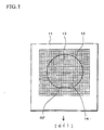
- FIG. 1 shows a conventional alignment of a GaAs wafer 12 with respect to a mask 11 having individual chip patterns 13.
- the GaAs wafer 12 is positioned with respect to the mask 11 using an orientation flat OF of the GaAs wafer as a positioning reference.
- an edge of the mask 11 and the orientation flat OF is aligned so that the two directions are parallel to each other or perpendicular to each other.
- all the chip patterns are aligned in directions parallel to and perpendicular to the edge of the mask 11.
- the orientation flat OF is generally formed in a direction normal to a [0 ⁇ ⁇ ] direction of the GaAs lattice.
- the surface of the GaAs wafer 12 is a (1 0 0) plane of the GaAs lattice and is exposed in a photolithographic process to form semiconductor devices such as GaAs FETs.
- the notation of surfaces and planes described in this specification is based on Miller indices.
- a dicing blade is first positioned on a dicing region 14 formed on the primary plane of the GaAs wafer 12, and then cuts the GaAs wafer 12 along the dicing region 14. Because of chipping, a typical width of the dicing region 14 is 50 ⁇ m. Other operational parameters of dicing blades in this process include a cutting speed of about 6 mm/sec and a blade spin rate of about 30000 to 35000 rpm. After dicing, the GaAs wafer 12 which have been cut by the dicing blade is rinsed with water and then dried before being sent to a bonding process.
- the wafer is diced in a direction parallel to or normal to the [0 ⁇ ⁇ ] direction of the wafer.
- the cleavage direction is either parallel to or normal to the [0 ⁇ ⁇ ] direction.
- the GaAs wafer 12 when the GaAs wafer 12 is diced along this direction, a large amount of chipping occurs along this direction because of the cleavage induced by stresses generated at a contact between the rotating dicing blade and the surface of the GaAs wafer 12. Chipping is a crack formation at the surface cut by the dicing blade and leads to reduced yield of the manufacturing process. Because of the chipping, the width of the dicing region 14 should be wider than otherwise required, or the cutting speed should be slow so as not to induce a large amount of chipping.
- the solution according to the invention lies in the features of the independent claims and preferably in those of the dependent claims.
- the invention provides a manufacturing method of compound semiconductor device including providing a compound semiconductor wafer having an orientation flat and providing a mask having individual chip patterns. This is followed by positioning the mask with respect to the wafer so that the individual chip patterns of the mask are aligned in a direction slanting with respect to the orientation flat. The method further includes patterning the wafer using the mask positioned with respect to the wafer and dicing the patterned wafer.
- the invention also provides a manufacturing method of compound semiconductor device including providing a compound semiconductor wafer having an orientation flat and providing a mask having individual chip patterns. This is followed by positioning the mask with respect to the wafer so that the individual chip patterns of the mask are aligned in a direction slanting by an angle between 30 and 60 degrees with respect to the orientation flat. The method further includes patterning the wafer using the mask positioned with respect to the wafer and dicing the patterned wafer in the direction slanting by an angle between 30 and 60 degrees with respect to the orientation flat.
- the invention further provides a compound semiconductor device including a compound semiconductor substrate having a substantially rectangular shape.
- a primary surface of the substrate has a (1 0 0) surface of a compound semiconductor or a crystallographically equivalent surface thereof.
- An edge of the substrate slants by an angle between 30 and 60 degrees with respect to a [0 1 1] direction of the compound semiconductor or a crystallographically equivalent direction thereof.
- the manufacturing method of this invention utilizes this characteristic of compound semiconductor substrate, and forms patterns on the substrate in this slanting direction and cuts the substrate in the same direction.
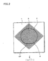
- FIG.2 shows an alignment of a mask 1 and a wafer 2 used in this embodiment.
- the mask 1 has chip patterns 3 for exposing circuit patterns onto a surface of the wafer 2 during a photolithographic process.
- the chip patterns 3 are adapted to align with a direction slanting by 45 degrees with respect to the direction of the orientation flat OF of the wafer 2 when the mask 1 is positioned over the wafer 2 for exposure.
- all the chip patterns 3 of the mask 1 are exposed onto the wafer 2 by a single exposure step.
- Each of the compound semiconductor device patterns, for example FET patterns, of the mask 1 is formed on a corresponding portion of a GaAs wafer at the same time.
- the mask itself 1 is automatically manufactured based on CAD data, and has chip patterns 3 slanting by 45 degrees with respect to the edge of the mask 1.
- the top surface of the wafer 2 is a (1 0 0) surface of GaAs having a zincblende lattice structure, and the orientation flat OF of the wafer 2 is cut in a direction normal to a [0 ⁇ ⁇ ] direction of GaAs, as denoted by an arrow shown in FIG. 2.
- the orientation flat OF is aligned in a direction parallel to one of the edges of the mask.
- the chip patterns 3 are aligned in a direction slanting by 45 degrees with respect to the orientation flat OF.
- the wafer 2 is diced in the direction slanting by 45 degrees with respect to the direction of the orientation flat OF of the wafer 2.
- the wafer 2 is, first, attached to a tape cut ring through a dicing sheet.
- a dicing blade is positioned on a dicing region 4 of the wafer 2, and cuts the primary plane of the wafer 2 in the direction of the dicing region, i.e., the direction slanting by 45 degrees with respect to the orientation flat OF.
- chipping is greatly reduced on all edges of the device chip. Accordingly, the width of the dicing region 4 is reduced by 10 ⁇ m to 40 ⁇ m in comparison to the conventional manufacturing method shown in FIG. 1.
- the cutting speed may be increased five to six times as high as that of conventional method.
- the wafer 2 was cut with dicing conditions including a cutting speed of about 30 to 40 mm/sec and a blade spin rate of about 30000 to 35000 rpm, which are similar to the dicing conditions of silicon wafer.
- the individual chips of the wafer 2 are separated from each other by expanding the dicing sheet, and rinsed with water. After drying, the individual chips are sent to the next process, i.e., a bonding process.
- dicing a primary surface of a compound semiconductor wafer having a (1 0 0) surface in a direction slanting by 45 degrees with respect to a [0 ⁇ ⁇ ] direction of the wafer greatly reduces chipping along all edges of the individual chips.
- the slanting angle between the alignment direction of the chip patterns and the orientation flat is 45 degrees.
- the slanting angle is not limited to this angle, but may be larger or smaller than this angle as long as the reduction of chipping is significantly reduced. For example, it maybe any angle between 30 and 60 degrees.
- the manufacturing method of this embodiment is not only applicable to formation of FETs on GaAs substrate, but also applicable to formation of MMIC and Schottky barrier diode, among other devices.
- the GaAs substrate may be replaced by other compound semiconductor substrate having a similar crystallographic structure.
Landscapes
- Dicing (AREA)
- Junction Field-Effect Transistors (AREA)
- Preparing Plates And Mask In Photomechanical Process (AREA)
- Exposure Of Semiconductors, Excluding Electron Or Ion Beam Exposure (AREA)
Abstract
In a method of manufacturing a compound semiconductor device,
individual chip patterns (3) are projected onto a (1 0 0)
surface of a GaAs wafer (2) so that the columns and rows of
the chip patterns (3) are aligned in a direction slanting by
45 degrees with respect to a [0 1 1] direction of the GaAs
wafer (2). The wafer (2) is diced along this slanting direction
and chipping along the edges of the individual separated
chips is greatly reduced.
Description
- The invention relates to a manufacturing method of compound semiconductor device operating at high frequencies, specifically to a method which prevents chipping of compound semiconductor substrate during dicing process, and a compound semiconductor device made by the manufacturing method.
- The demand for high frequency devices has been rapidly increasing due to the expanding market for portable telephones and digital satellite communication equipment. Many of such devices include field effect transistors (referred to as FET, hereinafter) employing a gallium arsenide (referred to as GaAs, hereinafter) substrate because of its excellent high frequency characteristics. Typical application in this field includes local oscillation FETs and monolithic microwave integrated circuits (MMIC) in which a plurality of FETs are integrated.
- In a typical semiconductor device manufacturing process, a semiconductor wafer in which semiconductor devices have been formed must be separated into individual devices. The most popular method to cut the wafer is to use a dicing saw. Such a method is well know and described in may publications including Japanese Laid Open Patent Publication No. Sho 60-34827.
- FIG. 1 shows a conventional alignment of a GaAs wafer 12 with respect to a
mask 11 havingindividual chip patterns 13. The GaAswafer 12 is positioned with respect to themask 11 using an orientation flat OF of the GaAs wafer as a positioning reference. Specifically, an edge of themask 11 and the orientation flat OF is aligned so that the two directions are parallel to each other or perpendicular to each other. In such a configuration, all the chip patterns are aligned in directions parallel to and perpendicular to the edge of themask 11. As indicated by an arrow in FIG. 1, the orientation flat OF is generally formed in a direction normal to a [0 í í] direction of the GaAs lattice. The surface of the GaAswafer 12 is a (1 0 0) plane of the GaAs lattice and is exposed in a photolithographic process to form semiconductor devices such as GaAs FETs. The notation of surfaces and planes described in this specification is based on Miller indices. - During a dicing process of the GaAs wafer 12, a dicing blade is first positioned on a
dicing region 14 formed on the primary plane of theGaAs wafer 12, and then cuts the GaAs wafer 12 along thedicing region 14. Because of chipping, a typical width of thedicing region 14 is 50 µm. Other operational parameters of dicing blades in this process include a cutting speed of about 6 mm/sec and a blade spin rate of about 30000 to 35000 rpm. After dicing, the GaAs wafer 12 which have been cut by the dicing blade is rinsed with water and then dried before being sent to a bonding process. - According to this conventional alignment of the mask, the chip patterns and the wafer, the wafer is diced in a direction parallel to or normal to the [0 í í] direction of the wafer. On a (1 0 0) plane of the GaAs lattice, the cleavage direction is either parallel to or normal to the [0 í í] direction. Thus, when the wafer is cut along a direction parallel to the [0 í í] direction, cleavage may easily occur along a direction normal to the cutting direction. Accordingly, when the GaAs
wafer 12 is diced along this direction, a large amount of chipping occurs along this direction because of the cleavage induced by stresses generated at a contact between the rotating dicing blade and the surface of the GaAs wafer 12. Chipping is a crack formation at the surface cut by the dicing blade and leads to reduced yield of the manufacturing process. Because of the chipping, the width of thedicing region 14 should be wider than otherwise required, or the cutting speed should be slow so as not to induce a large amount of chipping. - It is an object of this invention to provide a method of manufacturing a compound semiconductor device that allows a higher yield.
- The solution according to the invention lies in the features of the independent claims and preferably in those of the dependent claims. The invention provides a manufacturing method of compound semiconductor device including providing a compound semiconductor wafer having an orientation flat and providing a mask having individual chip patterns. This is followed by positioning the mask with respect to the wafer so that the individual chip patterns of the mask are aligned in a direction slanting with respect to the orientation flat. The method further includes patterning the wafer using the mask positioned with respect to the wafer and dicing the patterned wafer.
- The invention also provides a manufacturing method of compound semiconductor device including providing a compound semiconductor wafer having an orientation flat and providing a mask having individual chip patterns. This is followed by positioning the mask with respect to the wafer so that the individual chip patterns of the mask are aligned in a direction slanting by an angle between 30 and 60 degrees with respect to the orientation flat. The method further includes patterning the wafer using the mask positioned with respect to the wafer and dicing the patterned wafer in the direction slanting by an angle between 30 and 60 degrees with respect to the orientation flat.
- The invention further provides a compound semiconductor device including a compound semiconductor substrate having a substantially rectangular shape. A primary surface of the substrate has a (1 0 0) surface of a compound semiconductor or a crystallographically equivalent surface thereof. An edge of the substrate slants by an angle between 30 and 60 degrees with respect to a [0 1 1] direction of the compound semiconductor or a crystallographically equivalent direction thereof.
-
- FIG. 1
- shows an alignment of a mask and a wafer used in a conventional method of manufacturing compound semiconductor device.
- FIG. 2
- shows an alignment of a mask and a wafer used in an embodiment of a method of manufacturing compound semiconductor device of this invention.
- It is known in the art that chipping of a compound semicond-cutor substrate is greatly reduced when the substrate is diced along a direction slanting by 45 degrees with respect to a cleavage direction. Accordingly, the manufacturing method of this invention utilizes this characteristic of compound semiconductor substrate, and forms patterns on the substrate in this slanting direction and cuts the substrate in the same direction.
- An embodiment of a manufacturing method of compound semiconductor device of this invention is described with reference to FIG.2, which shows an alignment of a
mask 1 and awafer 2 used in this embodiment. Themask 1 haschip patterns 3 for exposing circuit patterns onto a surface of thewafer 2 during a photolithographic process. Thechip patterns 3 are adapted to align with a direction slanting by 45 degrees with respect to the direction of the orientation flat OF of thewafer 2 when themask 1 is positioned over thewafer 2 for exposure. - In this embodiment, all the
chip patterns 3 of themask 1 are exposed onto thewafer 2 by a single exposure step. Each of the compound semiconductor device patterns, for example FET patterns, of themask 1 is formed on a corresponding portion of a GaAs wafer at the same time. The mask itself 1 is automatically manufactured based on CAD data, and haschip patterns 3 slanting by 45 degrees with respect to the edge of themask 1. - The top surface of the
wafer 2 is a (1 0 0) surface of GaAs having a zincblende lattice structure, and the orientation flat OF of thewafer 2 is cut in a direction normal to a [0 í í] direction of GaAs, as denoted by an arrow shown in FIG. 2. - During the exposure step, the orientation flat OF is aligned in a direction parallel to one of the edges of the mask. In other words, the
chip patterns 3 are aligned in a direction slanting by 45 degrees with respect to the orientation flat OF. - After completion of device formation on the surface of the
wafer 2 following the exposure step, thewafer 2 is diced in the direction slanting by 45 degrees with respect to the direction of the orientation flat OF of thewafer 2. In this step, thewafer 2 is, first, attached to a tape cut ring through a dicing sheet. Then, a dicing blade is positioned on a dicing region 4 of thewafer 2, and cuts the primary plane of thewafer 2 in the direction of the dicing region, i.e., the direction slanting by 45 degrees with respect to the orientation flat OF. When thewafer 2 is cut along this direction, chipping is greatly reduced on all edges of the device chip. Accordingly, the width of the dicing region 4 is reduced by 10 µm to 40 µm in comparison to the conventional manufacturing method shown in FIG. 1. - Furthermore, the cutting speed may be increased five to six times as high as that of conventional method. In this embodiment, the
wafer 2 was cut with dicing conditions including a cutting speed of about 30 to 40 mm/sec and a blade spin rate of about 30000 to 35000 rpm, which are similar to the dicing conditions of silicon wafer. - After the dicing step, the individual chips of the
wafer 2 are separated from each other by expanding the dicing sheet, and rinsed with water. After drying, the individual chips are sent to the next process, i.e., a bonding process. - As described above, dicing a primary surface of a compound semiconductor wafer having a (1 0 0) surface in a direction slanting by 45 degrees with respect to a [0 í í] direction of the wafer greatly reduces chipping along all edges of the individual chips. There is no need for specially manufactured wafers having different crystallographic orientation, or specially designed exposure apparatus. Accordingly, overall production yield increases because of reduced chipping, and effective use of expensive compound semiconductor wafer is achieved because of narrower dicing region. Furthermore, narrowing of the dicing region leads to smaller size of the device.
- In this embodiment, the slanting angle between the alignment direction of the chip patterns and the orientation flat is 45 degrees. However, the slanting angle is not limited to this angle, but may be larger or smaller than this angle as long as the reduction of chipping is significantly reduced. For example, it maybe any angle between 30 and 60 degrees. Furthermore, the manufacturing method of this embodiment is not only applicable to formation of FETs on GaAs substrate, but also applicable to formation of MMIC and Schottky barrier diode, among other devices. The GaAs substrate may be replaced by other compound semiconductor substrate having a similar crystallographic structure.
- The above is a detailed description of a particular embodiment of the invention which is not intended to limit the invention to the embodiment described. It is recognized that modifications within the scope of the invention will occur to a person skilled in the art. Such modifications and equivalents of the invention are intended for inclusion within the scope of this invention.
Claims (9)
- A manufacturing method of compound semiconductor device comprising:providing a compound semiconductor wafer (2) having an orientation flat;providing a mask (1) having individual chip patterns (3);positioning the mask (1) with respect to the wafer (2) so that the individual chip patterns (3) of the mask (1) are aligned in a direction slanting with respect to the orientation flat;patterning the wafer (2) using the mask (1) positioned with respect to the wafer (2); anddicing the patterned wafer (2).
- The manufacturing method of compound semiconductor device of claim 1, whereina primary surface of the wafer (2) comprises a (1 0 0) surface of a compound semiconductor or a crystallographically equivalent surface thereof,the orientation flat is formed normal to a [0 1 1] direction of the compound semiconductor or a crystallographically equivalent direction thereof, andthe positioning of the mask (1) comprises aligning the orientation flat in a same direction as an edge of the mask (1) or aligning the orientation flat in a direction normal to the edge of the mask (1).
- A manufacturing method of compound semiconductor device comprising:providing a compound semiconductor wafer (2) having an orientation flat;providing a mask (1) having individual chip patterns (3);positioning the mask (1) with respect to the wafer (2) so that the individual chip patterns (3) of the mask (1) are aligned in a direction slanting by an angle between 30 and 60 degrees with respect to the orientation flat;patterning the wafer (2) using the mask (1) positioned with respect to the wafer (2); anddicing the patterned wafer (2) in the direction slanting by an angle between 30 and 60 degrees with respect to the orientation flat.
- The manufacturing method of compound semiconductor device of claim 3, whereina primary surface of the wafer (2) comprises a (1 0 0) surface of a compound semiconductor or a crystallographically equivalent surface thereof,the orientation flat is formed normal to a [0 1 1] direction of the compound semiconductor or a crystallographically equivalent direction thereof, andthe positioning of the mask (1) comprises aligning the orientation flat in a same direction as an edge of the mask (1) or aligning the orientation flat in a direction normal to the edge of the mask (1).
- The manufacturing method of compound semiconductor device of claim 4, wherein the compound semiconductor comprises GaAs.
- The manufacturing method of compound semiconductor device of claim 4, wherein the compound semiconductor comprises a zincblende lattice.
- A compound semiconductor device comprising a compound semiconductor substrate having a substantially rectangular shape, whereina primary surface of the substrate comprises a (1 0 0) surface of a compound semiconductor or a crystallographically equivalent surface thereof, andan edge of the substrate slants by an angle between 30 and 60 degrees with respect to a [0 1 1] direction of the compound semiconductor or a crystallographically equivalent direction thereof.
- The compound semiconductor device of claim 7, wherein the compound semiconductor comprises GaAs.
- The compound semiconductor device of claim 7, wherein the compound semiconductor comprises a zincblende lattice.
Applications Claiming Priority (2)
| Application Number | Priority Date | Filing Date | Title |
|---|---|---|---|
| JP2001207651A JP2003022987A (en) | 2001-07-09 | 2001-07-09 | Method for manufacturing compound semiconductor device |
| JP2001207651 | 2001-07-09 |
Publications (1)
| Publication Number | Publication Date |
|---|---|
| EP1278236A1 true EP1278236A1 (en) | 2003-01-22 |
Family
ID=19043605
Family Applications (1)
| Application Number | Title | Priority Date | Filing Date |
|---|---|---|---|
| EP02014979A Withdrawn EP1278236A1 (en) | 2001-07-09 | 2002-07-09 | Method of dicing a compound semiconductor wafer and compound semiconductor substrate thereby formed |
Country Status (6)
| Country | Link |
|---|---|
| US (2) | US6897126B2 (en) |
| EP (1) | EP1278236A1 (en) |
| JP (1) | JP2003022987A (en) |
| KR (1) | KR100620928B1 (en) |
| CN (1) | CN100466170C (en) |
| TW (1) | TWI266425B (en) |
Cited By (2)
| Publication number | Priority date | Publication date | Assignee | Title |
|---|---|---|---|---|
| EP1973174A3 (en) * | 2007-03-20 | 2010-07-21 | Sanyo Electric Co., Ltd. | Method for fracturing semiconductor substrate, method for fracturing solar cell, and the solar cell |
| CN110534422A (en) * | 2018-05-25 | 2019-12-03 | 力成科技股份有限公司 | Wafer processing method with full edge cutting |
Families Citing this family (18)
| Publication number | Priority date | Publication date | Assignee | Title |
|---|---|---|---|---|
| US20040219443A1 (en) * | 2003-05-01 | 2004-11-04 | Spears Kurt E. | Method for wafer dicing |
| JP2005042133A (en) * | 2003-07-22 | 2005-02-17 | Seiko Epson Corp | Vapor deposition mask and manufacturing method thereof, display device and manufacturing method thereof, and electronic apparatus including display device |
| FR2863771B1 (en) * | 2003-12-10 | 2007-03-02 | Soitec Silicon On Insulator | PROCESS FOR PROCESSING A MULTILAYER WAFER HAVING A DIFFERENTIAL OF THERMAL CHARACTERISTICS |
| US20050236616A1 (en) * | 2004-04-26 | 2005-10-27 | Horng-Huei Tseng | Reliable semiconductor structure and method for fabricating |
| JP4018096B2 (en) * | 2004-10-05 | 2007-12-05 | 松下電器産業株式会社 | Semiconductor wafer dividing method and semiconductor element manufacturing method |
| JP4438710B2 (en) * | 2005-07-20 | 2010-03-24 | セイコーエプソン株式会社 | Mask, mask chip, mask manufacturing method, and mask chip manufacturing method |
| JP4743661B2 (en) * | 2006-03-07 | 2011-08-10 | 信越半導体株式会社 | Light emitting device manufacturing method and light emitting device |
| JP2008028139A (en) * | 2006-07-21 | 2008-02-07 | Ricoh Co Ltd | Semiconductor chip manufacturing method, surface emitting semiconductor laser, surface emitting semiconductor laser array, optical scanning device, and image forming apparatus |
| US8389099B1 (en) | 2007-06-01 | 2013-03-05 | Rubicon Technology, Inc. | Asymmetrical wafer configurations and method for creating the same |
| JP2009043913A (en) * | 2007-08-08 | 2009-02-26 | Rohm Co Ltd | Semiconductor device and manufacturing method of semiconductor device |
| KR100901512B1 (en) * | 2007-10-30 | 2009-06-08 | 삼성전기주식회사 | PCB Strip |
| KR101016317B1 (en) * | 2008-12-01 | 2011-02-18 | (주)더리즈 | Chip manufacturing method of semiconductor element and wafer used for the method |
| JP5724342B2 (en) * | 2009-12-10 | 2015-05-27 | 大日本印刷株式会社 | Pattern arrangement method, silicon wafer and semiconductor device manufacturing method |
| JP5434547B2 (en) * | 2009-12-10 | 2014-03-05 | 大日本印刷株式会社 | Method for forming a plurality of patterns using a reticle |
| US20120313213A1 (en) * | 2011-06-07 | 2012-12-13 | Raytheon Company | Polygon shaped power amplifier chips |
| JP6654435B2 (en) * | 2016-01-07 | 2020-02-26 | 株式会社ディスコ | Wafer generation method |
| CN107180790B (en) * | 2017-06-29 | 2020-07-17 | 华进半导体封装先导技术研发中心有限公司 | Wafer cutting time calculation method and device |
| US20230290684A1 (en) * | 2022-03-09 | 2023-09-14 | Micron Technology, Inc. | Structures and methods for dicing semiconductor devices |
Citations (6)
| Publication number | Priority date | Publication date | Assignee | Title |
|---|---|---|---|---|
| JPS61263124A (en) * | 1985-05-16 | 1986-11-21 | Rohm Co Ltd | Mask plate for manufacturing semiconductor device |
| JPH02192753A (en) * | 1989-01-20 | 1990-07-30 | Fujitsu Ltd | Dividing method of compound semiconductor substrate |
| JPH03218050A (en) * | 1990-01-23 | 1991-09-25 | Matsushita Electric Ind Co Ltd | Gallium arsenic diode |
| US5182233A (en) * | 1989-08-02 | 1993-01-26 | Kabushiki Kaisha Toshiba | Compound semiconductor pellet, and method for dicing compound semiconductor wafer |
| EP0562880A1 (en) * | 1992-03-26 | 1993-09-29 | Nec Corporation | Semiconductor infrared emitting device with oblique side surface with respect to the cleavage and process of fabrication thereof |
| JPH05285935A (en) * | 1992-04-13 | 1993-11-02 | Sumitomo Electric Ind Ltd | Method of dividing semiconductor substrate |
Family Cites Families (4)
| Publication number | Priority date | Publication date | Assignee | Title |
|---|---|---|---|---|
| JPH0722122B2 (en) * | 1986-03-27 | 1995-03-08 | 沖電気工業株式会社 | Method for manufacturing semiconductor substrate |
| JPS63104348A (en) * | 1986-10-21 | 1988-05-09 | Toko Inc | Semiconductor device |
| JP3146874B2 (en) * | 1994-09-13 | 2001-03-19 | 三菱化学株式会社 | Light emitting diode |
| JPH0888201A (en) * | 1994-09-16 | 1996-04-02 | Toyoda Gosei Co Ltd | Semiconductor device using sapphire as substrate |
-
2001
- 2001-07-09 JP JP2001207651A patent/JP2003022987A/en active Pending
-
2002
- 2002-06-04 TW TW091111930A patent/TWI266425B/en not_active IP Right Cessation
- 2002-07-08 KR KR1020020039286A patent/KR100620928B1/en not_active Expired - Fee Related
- 2002-07-08 US US10/189,775 patent/US6897126B2/en not_active Expired - Lifetime
- 2002-07-09 CN CNB021409056A patent/CN100466170C/en not_active Expired - Fee Related
- 2002-07-09 EP EP02014979A patent/EP1278236A1/en not_active Withdrawn
- 2002-12-26 US US10/328,022 patent/US20030129788A1/en not_active Abandoned
Patent Citations (6)
| Publication number | Priority date | Publication date | Assignee | Title |
|---|---|---|---|---|
| JPS61263124A (en) * | 1985-05-16 | 1986-11-21 | Rohm Co Ltd | Mask plate for manufacturing semiconductor device |
| JPH02192753A (en) * | 1989-01-20 | 1990-07-30 | Fujitsu Ltd | Dividing method of compound semiconductor substrate |
| US5182233A (en) * | 1989-08-02 | 1993-01-26 | Kabushiki Kaisha Toshiba | Compound semiconductor pellet, and method for dicing compound semiconductor wafer |
| JPH03218050A (en) * | 1990-01-23 | 1991-09-25 | Matsushita Electric Ind Co Ltd | Gallium arsenic diode |
| EP0562880A1 (en) * | 1992-03-26 | 1993-09-29 | Nec Corporation | Semiconductor infrared emitting device with oblique side surface with respect to the cleavage and process of fabrication thereof |
| JPH05285935A (en) * | 1992-04-13 | 1993-11-02 | Sumitomo Electric Ind Ltd | Method of dividing semiconductor substrate |
Non-Patent Citations (4)
| Title |
|---|
| PATENT ABSTRACTS OF JAPAN vol. 011, no. 117 (E - 498) 11 April 1987 (1987-04-11) * |
| PATENT ABSTRACTS OF JAPAN vol. 014, no. 471 (E - 0990) 15 October 1990 (1990-10-15) * |
| PATENT ABSTRACTS OF JAPAN vol. 015, no. 498 (E - 1146) 17 December 1991 (1991-12-17) * |
| PATENT ABSTRACTS OF JAPAN vol. 018, no. 065 (M - 1554) 3 February 1994 (1994-02-03) * |
Cited By (4)
| Publication number | Priority date | Publication date | Assignee | Title |
|---|---|---|---|---|
| EP1973174A3 (en) * | 2007-03-20 | 2010-07-21 | Sanyo Electric Co., Ltd. | Method for fracturing semiconductor substrate, method for fracturing solar cell, and the solar cell |
| US8389320B2 (en) | 2007-03-20 | 2013-03-05 | Sanyo Electric Co., Ltd. | Method for fracturing semiconductor substrate, method for fracturing solar cell, and the solar cell |
| US8513047B2 (en) | 2007-03-20 | 2013-08-20 | Sanyo Electric Co., Ltd. | Method for fracturing semiconductor substrate, method for fracturing solar cell, and the solar cell |
| CN110534422A (en) * | 2018-05-25 | 2019-12-03 | 力成科技股份有限公司 | Wafer processing method with full edge cutting |
Also Published As
| Publication number | Publication date |
|---|---|
| TWI266425B (en) | 2006-11-11 |
| JP2003022987A (en) | 2003-01-24 |
| US20030017644A1 (en) | 2003-01-23 |
| US20030129788A1 (en) | 2003-07-10 |
| KR20030007047A (en) | 2003-01-23 |
| KR100620928B1 (en) | 2006-09-13 |
| US6897126B2 (en) | 2005-05-24 |
| CN1396628A (en) | 2003-02-12 |
| CN100466170C (en) | 2009-03-04 |
Similar Documents
| Publication | Publication Date | Title |
|---|---|---|
| US6897126B2 (en) | Semiconductor device manufacturing method using mask slanting from orientation flat | |
| US6955947B2 (en) | Backside metallization on microelectronic dice having beveled sides for effective thermal contact with heat dissipation devices | |
| US7064014B2 (en) | Backside metallization on sides of microelectronic dice for effective thermal contact with heat dissipation devices | |
| JP2780618B2 (en) | Method of manufacturing gallium nitride based compound semiconductor chip | |
| JP2009099681A (en) | Substrate separation method | |
| US6887771B2 (en) | Semiconductor device and method for fabricating the same | |
| JP2861991B2 (en) | Method of manufacturing gallium nitride based compound semiconductor chip | |
| JPH08293476A (en) | Method for manufacturing semiconductor integrated circuit device, semiconductor wafer, and photomask | |
| JP3227287B2 (en) | Method of manufacturing gallium nitride-based compound semiconductor chip and gallium nitride-based compound semiconductor device | |
| US6214639B1 (en) | Method of producing a semiconductor device | |
| EP1278235A1 (en) | Manufacturing method of compound semiconductor device | |
| JPH0774131A (en) | Dicing device and semiconductor chip processing method | |
| JP2718901B2 (en) | Method for manufacturing semiconductor device | |
| JPH05285935A (en) | Method of dividing semiconductor substrate | |
| JPH06188311A (en) | Semiconductor-element cutting method | |
| JP3454355B2 (en) | Gallium nitride based compound semiconductor light emitting device | |
| US20050266661A1 (en) | Semiconductor wafer with ditched scribe street | |
| US20250192090A1 (en) | Semiconductor devices with sidewall recesses | |
| US20240105514A1 (en) | Method of singulation of dies from a wafer | |
| JPH01133703A (en) | Semiconductor wafer and semiconductor device using the same | |
| TW202611998A (en) | Semiconductor chip manufacturing methods, wafer stacking, and semiconductor chips | |
| CN121941287A (en) | Semiconductor die and method for manufacturing the same | |
| CN120149266A (en) | Etch die cutting system and related methods | |
| JP2001217209A (en) | Semiconductor device, method of manufacturing the same, and wireless communication system | |
| JP2003078164A (en) | Gallium nitride based compound semiconductor light emitting device |
Legal Events
| Date | Code | Title | Description |
|---|---|---|---|
| PUAI | Public reference made under article 153(3) epc to a published international application that has entered the european phase |
Free format text: ORIGINAL CODE: 0009012 |
|
| AK | Designated contracting states |
Kind code of ref document: A1 Designated state(s): AT BE BG CH CY CZ DE DK EE ES FI FR GB GR IE IT LI LU MC NL PT SE SK TR |
|
| AX | Request for extension of the european patent |
Free format text: AL;LT;LV;MK;RO;SI |
|
| 17P | Request for examination filed |
Effective date: 20030327 |
|
| AKX | Designation fees paid |
Designated state(s): DE FR GB |
|
| STAA | Information on the status of an ep patent application or granted ep patent |
Free format text: STATUS: THE APPLICATION HAS BEEN WITHDRAWN |
|
| 18W | Application withdrawn |
Effective date: 20090811 |