EP1276244A2 - Composite high-frequency switch, high-frequency module, and communication apparatus - Google Patents
Composite high-frequency switch, high-frequency module, and communication apparatus Download PDFInfo
- Publication number
- EP1276244A2 EP1276244A2 EP02015384A EP02015384A EP1276244A2 EP 1276244 A2 EP1276244 A2 EP 1276244A2 EP 02015384 A EP02015384 A EP 02015384A EP 02015384 A EP02015384 A EP 02015384A EP 1276244 A2 EP1276244 A2 EP 1276244A2
- Authority
- EP
- European Patent Office
- Prior art keywords
- terminal
- frequency switch
- frequency
- diode
- transmission line
- Prior art date
- Legal status (The legal status is an assumption and is not a legal conclusion. Google has not performed a legal analysis and makes no representation as to the accuracy of the status listed.)
- Ceased
Links
Images




Classifications
-
- H—ELECTRICITY
- H04—ELECTRIC COMMUNICATION TECHNIQUE
- H04B—TRANSMISSION
- H04B1/00—Details of transmission systems, not covered by a single one of groups H04B3/00 - H04B13/00; Details of transmission systems not characterised by the medium used for transmission
- H04B1/38—Transceivers, i.e. devices in which transmitter and receiver form a structural unit and in which at least one part is used for functions of transmitting and receiving
- H04B1/40—Circuits
- H04B1/44—Transmit/receive switching
-
- H—ELECTRICITY
- H04—ELECTRIC COMMUNICATION TECHNIQUE
- H04B—TRANSMISSION
- H04B1/00—Details of transmission systems, not covered by a single one of groups H04B3/00 - H04B13/00; Details of transmission systems not characterised by the medium used for transmission
- H04B1/38—Transceivers, i.e. devices in which transmitter and receiver form a structural unit and in which at least one part is used for functions of transmitting and receiving
- H04B1/40—Circuits
- H04B1/44—Transmit/receive switching
- H04B1/48—Transmit/receive switching in circuits for connecting transmitter and receiver to a common transmission path, e.g. by energy of transmitter
Definitions
- the anode of a first diode is connected to the antenna terminal side and its cathode is connected to the transmission terminal side, and an inductor is connected between the cathode and a ground.
- the transmission line is connected between an antenna terminal and a receiving terminal, and the cathode of a second diode is connected to the receiving terminal side and a capacitor is connected between the anode of the second diode and a ground.
- a control terminal is connected between the second diode and the capacitor.
- preferred embodiments of the present invention provide a composite high-frequency switch and a high-frequency module which prevents distortion in first and second diodes of a communication system which is not selected without providing a negative power source, and a communication apparatus including the high-frequency module.
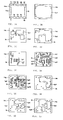
- the composite high-frequency switch according to preferred embodiments of the present invention further includes a multilayer substrate having a plurality of sheet layers layered thereon, wherein a diode of the high-frequency switch is mounted on the multilayer substrate, and a transmission line of the high-frequency switch is provided in the multilayer substrate.
- a forward bias is applied to the first and second diodes of the high-frequency switch on the selected communication system side, and at the same time, a reverse bias is applied to the first and second diodes of a high-frequency switch on the communication system side which is not selected.
- the distortion characteristics of the high-frequency module are also greatly improved.
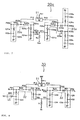
- the high-frequency switch 12 includes first and second diodes D21 and D22, a transmission line TL21, inductors L21 and L22, and a capacitor C21.
- the first diode D21, the transmission line TL21, the first diode D21, and the second terminal P22 are connected in series. Furthermore, the first terminal P21 side of the transmission line TL21 is connected to a ground via the second diode D22 and the capacitor C21, and a first control terminal V21 is connected to the ground side of the second diode D22, that is, the anode thereof, via the inductor L21.
- a second control terminal V22 is connected to the second terminal P22 side of the first diode D21, that is, the cathode thereof, via the inductor L22.
- a third terminal P23 is provided between the transmission line TL21 and the first diode D21.
- the second control terminal V22 of the high-frequency switch 12 and a second control terminal V32 of the high-frequency switch 13 are connected to each other, and a connection point thereof is connected to a common control terminal Vc via a resistor R.
- an antenna ANT is connected to the first terminal P11 of the diplexer 11, the third terminal P23 of the high-frequency switch 12 is connected to the second terminal P12, and a third terminal P33 of the high-frequency switch 13 is connected to the third terminal P13. Furthermore, a receiving circuit Rx is connected to the first terminal P21 of the high-frequency switch 12 and a first terminal P31 of the high-frequency switch 13, and a transmission circuit Tx is connected to the second terminal P22 of the high-frequency switch 12 and a second terminal P32 of the high-frequency switch 13.
- a forward bias is applied to the first and second diodes D21 and D22 of the high-frequency switch 12 on the selected communication system side, and forward current flows from the first control terminal V21 of the high-frequency switch 12 toward the common control terminal Vc.
- the amount of the voltage drop is applied as a reverse bias to the first and second diodes D31 and D32 of the high-frequency switch 13.
- This reverse bias causes the off capacity of the first and second diodes D31 and D32 of the high-frequency switch 13 on the communication system side which is not selected to be stabilized and decreased. As a consequence, the distortion characteristics are greatly improved.
- the inductor shields a high-frequency signal.
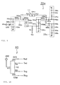
- Fig. 7 is a circuit diagram showing a modification of the high-frequency module of Fig. 6.
- a high-frequency module 20a is designed for a triple band and is defined by the diplexer 11 and the high-frequency switches 22a and 23a.
- the structure of the diplexer 11 is the same as that of the high-frequency module 10 (Fig. 1) of the first preferred embodiment, and accordingly, a description thereof is omitted.
Landscapes
- Engineering & Computer Science (AREA)
- Computer Networks & Wireless Communication (AREA)
- Signal Processing (AREA)
- Transceivers (AREA)
- Waveguide Switches, Polarizers, And Phase Shifters (AREA)
- Transmitters (AREA)
Abstract
Description
Claims (21)
- A composite high-frequency switch comprising:a plurality of high-frequency switches (12, 13), each including a first terminal (P21, P31), a second terminal (P22, P32), a first control terminal (V21, V31), a second control terminal (V22, V32), a first diode (D21, D31), a second diode (D22, D32), and a transmission line (TL21, TL 31); whereinthe composite high-frequency switch is arranged such that the first terminal (P21, P31), the transmission line (TL21, TL 31), the first diode (D21, D31), and the second terminal (P22, P32) are connected in series, the first terminal (P21, P31) side of the transmission line (TL21, TL31) is connected to a ground via the second diode (D22, D32), the first control terminal (V21, V31) is connected to the ground side of the second diode (D22, D32), and the second control terminal (V22, V32) is connected to the second terminal (P22, P32) side of the first diode (D21, D31); andat least two of the plurality of high-frequency switches (12, 13) are arranged such that the second control terminals (V22, V32) are connected to each other and the connection point thereof is connected to a common control terminal (Vc) via a resistor (R).
- A composite high-frequency switch according to Claim 1, further comprising a multilayer substrate (14) having a plurality of sheet layers layered thereon, wherein a diode (D21, D31, D22, D32) of the composite high-frequency switch is mounted on the multilayer substrate (14), and a transmission line (TL21, TL31) of the composite high-frequency switch is provided in the multilayer substrate (14).
- A high-frequency module comprising:a composite high-frequency switch according to claim 1; anda diplexer (11) comprising an inductor (L11, L12) and a capacitor (C11 - C15), the diplexer (11) being connected to a connection point (P23, P33) of the first diode (D21, D31) and the transmission line (TL21, TL31) of the composite high-frequency switch.
- A high-frequency module according to Claim 3, further comprising a multilayer substrate (14) having a plurality of sheet layers layered thereon, wherein a diode (D21, D31, D22, D32) of the composite high-frequency switch is mounted on the multilayer substrate (14), and the inductor (L11, L12) and the capacitor (C11 - C15) of the diplexer, and a transmission line (TL21, TL31) of the high-frequency switch is provided in the multilayer substrate (14).
- A high-frequency module according to Claim 4, wherein the capacitor (C11 - C15) of the diplexer (11) is connected to the ground, and a grounding electrode of the composite high-frequency switch is provided between the capacitor (C11 - C15) and the transmission line (TL21, TL31) of the composite high-frequency switch.
- A communication apparatus comprising a composite high-frequency switch according to Claim 1.
- A communication apparatus comprising a high-frequency module according to Claim 3.
- A composite high-frequency switch, comprising:a plurality of high-frequency switches (12, 13), each including a first terminal (P21, P31), a second terminal (P22, P32), a first control terminal (V21, V31), a second control terminal (V22, V32), a first diode (D21, D31), a second diode (D22, D32), and a transmission line (TL21, TL31); whereinthe composite high-frequency switch is arranged such that the first terminal (P21, P31), the transmission line (TL21, TL31), the first diode (D21, D31), and the second terminal (P22, P32) are connected in series, the first terminal (P21, P31) side of the transmission line (TL21, TL31) is connected to a ground via the second diode (D22, D32), the first control terminal is connected to the ground side of the second diode (D22, D32), the second control terminal (V22, V32) is connected to the second terminal (P22, P32) side of the first diode (D21, D31); andat least two of the plurality of high-frequency switches (12, 13) are arranged such that the first control terminals (V21, V31) are connected to each other and the connection point thereof is connected to a common control terminal (Vc) via a resistor (R).
- A composite high-frequency switch according to Claim 8, further comprising a multilayer substrate (14) having a plurality of sheet layers layered thereon, wherein a diode (D21, D31, D22, D32) of the composite high-frequency switch is mounted on the multilayer substrate (14), and a transmission line (TL21, TL31) of the high-frequency switch is provided in the multilayer substrate (14).
- A high-frequency module comprising:a composite high frequency switch according to Claim 8;a diplexer (11) comprising an inductor (L11, L12) and a capacitor (C11 - C15), the diplexer (11) being connected to a connection point (P23, P33) of the first diode (D21, D31) and the transmission line (TL21, TL31) of the composite high-frequency switch.
- A high-frequency module according to Claim 10, further comprising a multilayer substrate (14) having a plurality of sheet layers layered thereon, wherein a diode (D21, D31, D22, D32) of the composite high-frequency switch is mounted on the multilayer substrate (14), and the inductor (L11, L12) and the capacitor (C11 - C15) of the diplexer, and a transmission line (TL21, TL31) of the composite high-frequency switch is provided the multilayer substrate (14).
- A high-frequency module according to Claim 11, wherein the capacitor of the diplexer (11) is connected to the ground, and a grounding electrode of the composite high-frequency switch is provided between the capacitor (C11 - C15) and the transmission line (TL21, TL31) of the composite high-frequency switch.
- A communication apparatus comprising a composite high-frequency switch according to Claim 8.
- A communication apparatus comprising a composite high-frequency module according to Claim 10.
- A composite high-frequency switch, comprising:a plurality of high-frequency switches (12, 13) each having a first terminal (P21, P31), a second terminal (P22, P32), a first control terminal (V21, V31), a second control terminal (V22, V32), a first diode (D21, D31), a second diode (D22, D32), and a transmission line (TL21, TL31); whereinthe composite high-frequency switch is arranged such that the first terminal (P21, P31), the transmission line (TL21, TL31), the first diode (D21, D22), and the second terminal (P22, P32) are connected in series, the first terminal (P21, P31) side of the transmission line (TL21, TL31) is connected to a ground via the second diode (D22, D32), the first control terminal (V21, V31) is connected to the ground side of the second diode (D22, D32), the second control terminal (V22, V32) is connected to the second terminal (P22, P32) side of the first diode (D21, D31); andat least two of the plurality of high-frequency switches (12, 13) are arranged such that the first control terminal (V31) of a first of the high-frequency switches and the second control terminal (V22) of a second of the high-frequency switches are connected to each other and the connection point thereof is connected to a common control terminal (Vc) via a resistor (R).
- A composite high-frequency switch according to Claim 15, further comprising a multilayer substrate (14) having a plurality of sheet layers layered thereon, wherein a diode (D21, D31, D22, D32) of the composite high-frequency switch is mounted on the multilayer substrate (14), and a transmission line (TL21, TL31) of the composite high-frequency switch is provided in the multilayer substrate (14).
- A high-frequency module comprising:a composite high-frequency switch according to Claim 15;a diplexer (11) comprising an inductor (L11, L12) and a capacitor (C11 - C15), the diplexer (11) being connected to a connection point (P23, P33) of the first diode (D21, D31) and the transmission line (TL21, TL31) of the composite high-frequency switch.
- A high-frequency module according to Claim 17, further comprising a multilayer substrate (14) having a plurality of sheet layers layered thereon, wherein a diode (D21, D31, D22, D32) of the composite high-frequency switch is mounted on the multilayer substrate (14), and the inductor (L11, L12) and the capacitor (C11 - C15) of the diplexer, and a transmission line (TL21, TL31) of the high-frequency switch is provided in the multilayer substrate (14).
- A high-frequency module according to Claim 18, wherein the capacitor (C11 - C15) of the diplexer (11) is connected to the ground, and a grounding electrode of the composite high-frequency switch is provided between the capacitor (C11 - C15) and the transmission line (TL21, TL31) of the high-frequency switch.
- A communication apparatus comprising a composite high-frequency switch according to Claim 15.
- A communication apparatus comprising a high-frequency module according to Claim 17.
Applications Claiming Priority (2)
| Application Number | Priority Date | Filing Date | Title |
|---|---|---|---|
| JP2001213467A JP2003032001A (en) | 2001-07-13 | 2001-07-13 | Compound high frequency switch, high frequency module and communication device |
| JP2001213467 | 2001-07-13 |
Publications (2)
| Publication Number | Publication Date |
|---|---|
| EP1276244A2 true EP1276244A2 (en) | 2003-01-15 |
| EP1276244A3 EP1276244A3 (en) | 2004-03-03 |
Family
ID=19048435
Family Applications (1)
| Application Number | Title | Priority Date | Filing Date |
|---|---|---|---|
| EP02015384A Ceased EP1276244A3 (en) | 2001-07-13 | 2002-07-10 | Composite high-frequency switch, high-frequency module, and communication apparatus |
Country Status (5)
| Country | Link |
|---|---|
| US (1) | US6639489B2 (en) |
| EP (1) | EP1276244A3 (en) |
| JP (1) | JP2003032001A (en) |
| KR (1) | KR100476279B1 (en) |
| CN (1) | CN1228924C (en) |
Cited By (1)
| Publication number | Priority date | Publication date | Assignee | Title |
|---|---|---|---|---|
| CN103155427A (en) * | 2010-09-29 | 2013-06-12 | 株式会社村田制作所 | High-frequency module |
Families Citing this family (16)
| Publication number | Priority date | Publication date | Assignee | Title |
|---|---|---|---|---|
| WO2004036778A1 (en) * | 2002-10-14 | 2004-04-29 | Koninklijke Philips Electronics N.V. | Transmit and receive antenna switch |
| DE102005034878B4 (en) * | 2004-07-26 | 2011-08-18 | Kyocera Corp. | Selector switch, radio frequency transceiver, radar device, vehicle equipped with the radar device, and small ship |
| JP3841097B2 (en) * | 2004-09-30 | 2006-11-01 | 株式会社村田製作所 | Manufacturing method of high frequency switch |
| KR100699200B1 (en) * | 2004-11-26 | 2007-03-27 | (주)이노알에스 | High speed, low loss time division duplex transmit and receive switching method |
| CN101128985A (en) * | 2005-08-26 | 2008-02-20 | 株式会社村田制作所 | high frequency switch |
| KR100842576B1 (en) * | 2005-09-08 | 2008-07-01 | 삼성전자주식회사 | Antenna device of mobile terminal |
| CN101573881B (en) * | 2006-12-21 | 2013-04-17 | 株式会社村田制作所 | High Frequency Switching Circuit |
| KR100843120B1 (en) * | 2007-05-18 | 2008-07-02 | (주)비씨엔이글로발 | Low Frequency Separator on Coaxial Line |
| WO2010101130A1 (en) * | 2009-03-03 | 2010-09-10 | 株式会社村田製作所 | High frequency module |
| US9887462B2 (en) * | 2013-10-31 | 2018-02-06 | Motorola Solutions, Inc. | Antenna with embedded wideband matching substrate |
| US10658222B2 (en) | 2015-01-16 | 2020-05-19 | Lam Research Corporation | Moveable edge coupling ring for edge process control during semiconductor wafer processing |
| US10651015B2 (en) | 2016-02-12 | 2020-05-12 | Lam Research Corporation | Variable depth edge ring for etch uniformity control |
| WO2019103722A1 (en) | 2017-11-21 | 2019-05-31 | Lam Research Corporation | Bottom and middle edge rings |
| CN118398464A (en) | 2018-08-13 | 2024-07-26 | 朗姆研究公司 | Replaceable and/or collapsible edge ring assembly incorporating edge ring positioning and centering functions for plasma sheath adjustment |
| CN115315775A (en) | 2020-03-23 | 2022-11-08 | 朗姆研究公司 | Medium ring corrosion compensation in substrate processing systems |
| JP7322792B2 (en) * | 2020-04-09 | 2023-08-08 | 住友電気工業株式会社 | High frequency switch circuit and front end circuit including the same |
Family Cites Families (15)
| Publication number | Priority date | Publication date | Assignee | Title |
|---|---|---|---|---|
| JP3031178B2 (en) * | 1994-09-28 | 2000-04-10 | 株式会社村田製作所 | Composite high frequency components |
| EP0720292B1 (en) * | 1994-12-29 | 2000-03-29 | Koninklijke Philips Electronics N.V. | Terminal device for mobile telecommunications including a switching circuit |
| US5999065A (en) * | 1995-08-24 | 1999-12-07 | Murata Manufacturing Co., Ltd. | Composite high-frequency component |
| JPH1032521A (en) * | 1996-07-17 | 1998-02-03 | Murata Mfg Co Ltd | Duplexer |
| JPH11168303A (en) | 1997-12-05 | 1999-06-22 | Hitachi Metals Ltd | High frequency switch module |
| JP3191213B2 (en) * | 1998-04-28 | 2001-07-23 | 日立金属株式会社 | High frequency switch module |
| DE19823049C2 (en) * | 1998-05-22 | 2000-09-21 | Ericsson Telefon Ab L M | Power amplifier output circuit for suppressing harmonics for a mobile radio unit with double band operation and method for operating the same |
| JP3304898B2 (en) * | 1998-11-20 | 2002-07-22 | 株式会社村田製作所 | Composite high frequency component and mobile communication device using the same |
| SE518416C2 (en) * | 1998-12-22 | 2002-10-08 | Ericsson Telefon Ab L M | Antenna Switch Module |
| JP2000196496A (en) * | 1998-12-30 | 2000-07-14 | Murata Mfg Co Ltd | High frequency switch |
| JP2001102957A (en) * | 1999-09-28 | 2001-04-13 | Murata Mfg Co Ltd | Composite high-frequency component and mobile communication device using same |
| US6542021B2 (en) * | 2000-01-20 | 2003-04-01 | Matsushita Electric Industrial Co., Ltd. | High frequency switch and communication apparatus with a high frequency voltage divider |
| JP3617399B2 (en) * | 2000-01-21 | 2005-02-02 | 株式会社村田製作所 | High frequency switch |
| US6586786B2 (en) * | 2000-12-27 | 2003-07-01 | Matsushita Electric Industrial Co., Ltd. | High frequency switch and mobile communication equipment |
| JP3874237B2 (en) * | 2001-01-09 | 2007-01-31 | 日立金属株式会社 | Low distortion high frequency switch module |
-
2001
- 2001-07-13 JP JP2001213467A patent/JP2003032001A/en active Pending
-
2002
- 2002-06-14 US US10/170,554 patent/US6639489B2/en not_active Expired - Lifetime
- 2002-07-10 EP EP02015384A patent/EP1276244A3/en not_active Ceased
- 2002-07-10 KR KR10-2002-0039950A patent/KR100476279B1/en not_active Expired - Lifetime
- 2002-07-12 CN CNB021264171A patent/CN1228924C/en not_active Expired - Lifetime
Cited By (2)
| Publication number | Priority date | Publication date | Assignee | Title |
|---|---|---|---|---|
| CN103155427A (en) * | 2010-09-29 | 2013-06-12 | 株式会社村田制作所 | High-frequency module |
| CN103155427B (en) * | 2010-09-29 | 2015-11-25 | 株式会社村田制作所 | High frequency module |
Also Published As
| Publication number | Publication date |
|---|---|
| CN1398048A (en) | 2003-02-19 |
| US20030021356A1 (en) | 2003-01-30 |
| KR100476279B1 (en) | 2005-03-16 |
| KR20030007095A (en) | 2003-01-23 |
| JP2003032001A (en) | 2003-01-31 |
| EP1276244A3 (en) | 2004-03-03 |
| CN1228924C (en) | 2005-11-23 |
| US6639489B2 (en) | 2003-10-28 |
Similar Documents
| Publication | Publication Date | Title |
|---|---|---|
| US6633748B1 (en) | Composite high frequency component and mobile communication device including the same | |
| EP1276244A2 (en) | Composite high-frequency switch, high-frequency module, and communication apparatus | |
| EP1089449B1 (en) | Matching connections in a multilayer substrate | |
| EP1311063B1 (en) | Diplexer, and high-frequency switch and antenna duplexer using the same | |
| JP4324814B2 (en) | High frequency switch circuit | |
| US7379751B2 (en) | Multi-band transceiver and radio communication device using the transceiver | |
| JP3371887B2 (en) | Mobile communication device and high-frequency composite component used therefor | |
| KR100757915B1 (en) | High frequency switch module | |
| JP2001345729A (en) | High frequency module and radio apparatus comprising it | |
| WO2000055983A1 (en) | High-frequency switch module | |
| JPWO2000055983A1 (en) | High Frequency Switch Module | |
| US7356349B2 (en) | High-frequency module and communication apparatus | |
| US20040130388A1 (en) | Electric circuit module, circuit module arrangement and use of said circuit module and of said circuit module arrangement | |
| JP3304901B2 (en) | Composite high frequency component and mobile communication device using the same | |
| JP3304931B2 (en) | Composite high frequency component and mobile communication device using the same | |
| JP3807615B2 (en) | Multiband antenna switch circuit | |
| US20010004353A1 (en) | High frequency composite component and mobile communication apparatus incorporating the same | |
| JP3304900B2 (en) | Composite high frequency component and mobile communication device using the same | |
| JP3874237B2 (en) | Low distortion high frequency switch module | |
| JP2003051758A (en) | Hybrid high frequency component and mobile communication device employing the same | |
| KR100833252B1 (en) | High frequency switch module and its control method | |
| JP2004320244A (en) | Multiband high-frequency signal transceiver module | |
| JP4126874B2 (en) | Composite high-frequency component and mobile communication device using the same | |
| JP4352612B2 (en) | Composite high-frequency component and mobile communication device using the same | |
| JP2003188762A (en) | Antenna switch module |
Legal Events
| Date | Code | Title | Description |
|---|---|---|---|
| PUAI | Public reference made under article 153(3) epc to a published international application that has entered the european phase |
Free format text: ORIGINAL CODE: 0009012 |
|
| 17P | Request for examination filed |
Effective date: 20020710 |
|
| AK | Designated contracting states |
Kind code of ref document: A2 Designated state(s): AT BE BG CH CY CZ DE DK EE ES FI FR GB GR IE IT LI LU MC NL PT SE SK TR |
|
| AX | Request for extension of the european patent |
Free format text: AL;LT;LV;MK;RO;SI |
|
| PUAL | Search report despatched |
Free format text: ORIGINAL CODE: 0009013 |
|
| AK | Designated contracting states |
Kind code of ref document: A3 Designated state(s): AT BE BG CH CY CZ DE DK EE ES FI FR GB GR IE IT LI LU MC NL PT SE SK TR |
|
| AX | Request for extension of the european patent |
Extension state: AL LT LV MK RO SI |
|
| RIC1 | Information provided on ipc code assigned before grant |
Ipc: 7H 04B 1/40 B Ipc: 7H 04B 1/44 B Ipc: 7H 04B 1/48 A |
|
| 17Q | First examination report despatched |
Effective date: 20040621 |
|
| AKX | Designation fees paid |
Designated state(s): DE FR GB |
|
| STAA | Information on the status of an ep patent application or granted ep patent |
Free format text: STATUS: THE APPLICATION HAS BEEN REFUSED |
|
| 18R | Application refused |
Effective date: 20060612 |