EP1274229A1 - Method for obtaining line synchronization information items from a video signal, and apparatus for carrying out the method - Google Patents
Method for obtaining line synchronization information items from a video signal, and apparatus for carrying out the method Download PDFInfo
- Publication number
- EP1274229A1 EP1274229A1 EP01401811A EP01401811A EP1274229A1 EP 1274229 A1 EP1274229 A1 EP 1274229A1 EP 01401811 A EP01401811 A EP 01401811A EP 01401811 A EP01401811 A EP 01401811A EP 1274229 A1 EP1274229 A1 EP 1274229A1
- Authority
- EP
- European Patent Office
- Prior art keywords
- line
- video
- signal
- video line
- sync
- Prior art date
- Legal status (The legal status is an assumption and is not a legal conclusion. Google has not performed a legal analysis and makes no representation as to the accuracy of the status listed.)
- Withdrawn
Links
Images


Classifications
-
- H—ELECTRICITY
- H04—ELECTRIC COMMUNICATION TECHNIQUE
- H04N—PICTORIAL COMMUNICATION, e.g. TELEVISION
- H04N5/00—Details of television systems
- H04N5/04—Synchronising
- H04N5/08—Separation of synchronising signals from picture signals
- H04N5/10—Separation of line synchronising signal from frame synchronising signal or vice versa
Definitions
- the invention relates to a method for obtaining line synchronization information items from a video signal. According to a second aspect the invention is related to an apparatus for generating a line synchronisation pulse for a video line signal.
- analogue source signals will still exist for many years in the future. Examples include the terrestrial reception of video signals, which is still widespread to date, and the analogue recording methods, e.g. according to the VHS standard in the case of video recorders.
- Such analogue signal sources represent critical signal sources for digital systems, and their signal processing requires special measures. The situation is the same for future multimedia terminals as long as they are equipped with an analogue video input. Due to the existence of large quantities of analogue video material, e.g. VHS tape libraries, it is unlikely that the use of analogue video signals could disappear in the near future.
- a sync slicer is used for sync separation.
- the sync slicer is combined with a PLL (Phase Locked Loop) for "smoothing" the extracted sync information.
- PLL Phase Locked Loop
- the PLL technology is mature but has well known limitations due to two conflicting requirements: On the one hand the PLL must have a low-pass characteristic to suppress disturbances in the sync signal detection caused by noise.
- tape recorders in particular camcorders, output the video signal on a variable time base due to mechanical tolerances.
- the time base variations also appear as disturbances of the sync signal to the PLL.
- this kind of disturbance has to be passed through without attenuation because any alterations of the time base would create horizontal instabilities of the displayed video picture.
- the PLL has to suppress noise on the one hand and has to pass time-base variations on the other hand. Fortunately, the two effects are distinguishable by their frequency. Time-base variations are a low frequency effect above 1 kHz. As the PLL is always a second order loop, corner frequencies and stability are selected in every new designed system for best compromise.
- TV receivers with digital signal processing have been operating, as a rule, with clock systems, which are synchronized with the respective input signal. Since the input signal is the analogue CVBS signal, either the horizontal sync pulse (line-locked clock) or, alternatively, the colour subcarriers or colour synchronizing pulses (burst) (colour subcarrier-locked clock) are frequently used as reference point for the synchronization.
- the sync separation in the video lines has usually been carried out to date by means of analogue methods using so-called sync separator stages and a PLL filter stage connected downstream.
- a PLL filter stage which is a digital realization of the known analogue sync signal processing is commonly used.
- the filter stage is then a digital PLL (Phase-Locked Loop).
- digital PLL Phase-Locked Loop
- Examples of such digital PLL circuits are the circuits SAA 7111 from Philips, HMP 8112 from Harris and Digit 3000 from Micronas.
- the principal problem with such digital PLL circuits is that the known instabilities in the picture occur when the input signal present is an analogue video signal picked off from an analogue video recorder, which is currently operating in the search mode (fast forward or reverse run). Many users of analogue video recorders are sufficiently acquainted with such instabilities. Specifically, disturbing horizontal stripes appear in the picture when the video recorder is operating in the search mode.
- EP-A 0 266 147 discloses a digital PLL circuit for a television receiver.
- this digital PLL circuit in order to avoid the abovementioned problem in the search operating mode in video recorders, a switching unit is provided which drastically shortens the time constant of the phase-locked loop in the event of identification of a sudden phase change caused by the head changeover at the end of a slanted track, with the result that the region of instability in the picture is reduced in size.
- the disadvantage of this solution is that the reduction of the time constant of the phase-locked loop provided by this solution means that noise components in the video signal are able to be suppressed less well and disturbing lines still remain visible, even though to a lesser extent than when the time constant is larger.
- EP-A 0 899 945 a method is for obtaining line synchronization information is described.
- a video line is convoluted with an idealized horizontal synchronization pulse.
- the result of the convolutions processed in an open loop system replacing the PLL.
- the open loop system is realized by a linear regression to extrapolate the best guess of a current sync pulse using past sync pulses.
- Convolving or convolution, is a well-known term meaning the integral of one function multiplied by another function, which is shifted in time, see for example in "New IEEE Standard Dictionary of Electrical and Electronics Terms", 1993.
- the present invention suggests a method for obtaining line synchronization information from a video line signal.
- the relevant part of the video line signal is analysed to determine time instants defining the temporal position of the line synchronization pulses.
- a predetermined number of video lines is stored in a line delay. Using this as a data base a filtered time instant for a video line preceding the currently received video line by the number of video lines stored in the line delay.
- the calculation is an interpolation of the time instants determined for video lines preceding and following the currently displayed video line.
- the interpolation is a linear interpolation.
- an apparatus for generating line synchronization pulses from a video line signal comprises means for analysing the entire or the relevant part of the video line to determine time instants defining the temporal position of the line synchronization pulses.
- the apparatus further includes a line delay for storing a number of video lines.
- means are provided for calculating a filtered time instant for a video line preceding the currently received video line by the number of video lines stored in the line delay.
- the apparatus comprises means for convolving the entire or the relevant part of the video line with a pattern function.
- the apparatus is provided with an FIR filter having a set of predetermined filter constants.
- Fig. 1 Simulated values for the position of the line sync pulses in a video signal are plotted in Fig. 1.
- the number of the respective line is plotted in the direction of the abscissa in Figure 1.
- the reciprocal of the current horizontal frequency 1/f H for the line sync pulses is plotted in the direction of the ordinate of Fig. 1.
- the letter "n" generally designates the line number of each video line.
- the plotting of the reciprocal of the current horizontal frequency means that the time-domain positions of the respective line sync pulses can be compared with one another.
- the values corresponding to the actual measured values for the individual positions of the line sync pulses are in each case specified by the broken vertical lines. The end of each broken vertical line then specifies the line sync pulse position established.
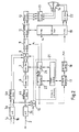
- Fig. 2 shows a top level diagram of the sync and video processing of a TV incorporating the present invention.
- the proposed architecture is based on a free running system clock, e.g. a crystal oscillator.
- the system clock has no correlation to the video sync or colour subcarrier frequencies.
- the free running system clock is particularly advantageous for processor-based systems adapted to receive video signals of various types and properties.
- colour burst-locked clocked systems are also possible to realize with the architecture described in the following if this is desirable for certain embodiments.
- Fig. 2 On the left hand side of Fig. 2 the inputs for analogue base band video signals are shown.
- the inputs 1a and 1b are used for S video signals having separate chrominance C and luminance Y inputs.
- the input 2 is provided for receiving composite video signals.
- the analogue video signals are converted into corresponding digital signals by A/D converters 3a and 3b, respectively.
- the digital output signals are then stored in FIFO (first-in-first-out) line delays 4a and 4b, respectively, having a size of e.g. eight video lines.
- the FIFO line delays are necessary for filtering time data used in horizontal sync processing, as it will be described further below.
- a comb filter is provided to separate the luminance Y and the chrominance C signals. Subsequently, the signals are fed into a chrominance decoder to generate the luminance signal Y and the chrominance signal C.
- a switch 8 is controlled to select the luminance and chrominance signals received from line delay 4a or from chroma decoder 7 to be further processed in a pixel interpolation filter 9, which will be described in more detail below.
- the output of filter 9 is buffered in a line buffer 11 and passed on to a colour dematrix 12 for generating digital R, G, B signals.
- the digital R, G, B signals are converted into analogue signals, amplified by associated drivers in block 13 and supplied to a cathode ray tube 14 for display.
- the signal processing may be different than shown in the present embodiment. However, these differences do not depart from the scope of the present invention.
- a digital luminance signal Y or a digital composite video signal is selectively used depending on which analogue inputs are active.
- the signal for sync signal processing is selected by switch 16 controlled by the same control signal as the switch 8.
- the vertical sync processing in block 17 is conventional and is therefore not described in more detail.
- the information regarding which field of a video frame is currently being processed is also obtained in this unit.
- the vertical sync signal V sync is delayed in a line delay 18 to re-establish the timing to the video signals delayed in the line delays 4a and 4b, respectively.
- the V sync signal is input to a microprocessor 19, which is among other functions operative to execute the synchronization logic.
- a H sync processing unit 21 the H sync signals are detected and processed by the inventive method, which will be described in more detail below.
- the horizontal sync information is supplied to the ⁇ P 19.
- the ⁇ P 19 uses the horizontal and vertical sync information to generate output signals for a deflection driver 22 being connected to a deflection apparatus not shown in Fig. 2.
- the deflection apparatus is associated with the CRT 14 and effects the scanning of the electron beams inside the CRT in a conventional way.
- the deflection driver 22 is replaced by an appropriate device effecting the representation of the video signal line by line on the screen of the respective display device.
- the H sync processing unit 21 comprises a H sync detector 23 to determine the timing of H sync signals contained in the received video signal.
- the H sync signals are filtered in a H-filter 24 and the resulting signals H o and ⁇ o are provided to the ⁇ P19 and to the pixel interpolation filter 9.
- the operation of the H sync detector 23, the H-filter 24 and the V sync processor 17 is controlled by an event control 25, which will be described in more detail in connection with Fig. 8.
- the present H sync detector 23 operates according to the correlation principle.
- the CVBS signal is convolved with an ideal line sync pulse and then the minimum is sought.
- This principle is illustrated in Fig. 3, where it is possible to discern in principle that the convolution operation of two square-wave pulses generates a triangle function as result function. This function then has a minimum or maximum, which specifies the position of the line sync pulse.
- the CVBS signal for a video line is designated by the reference symbol f in (k).
- the reference symbol s ideal (k) designates an ideal line sync pulse.
- the result function of the convolution operation is designated by the reference symbol ⁇ SV (k).
- the reference symbol k S specifies the position of the minimum of the result function.
- the convolution operation is carried out in the H sync detector 23 for example in such a way that the CVBS signal present in one of the line stores 4a, 4b for a video line is digitally convolved with a corresponding ideal line sync pulse.
- the execution may alternatively be configured in such a way that instead of the CVBS signal for the entire video line being convolved with the ideal line sync pulse, only the relevant part for the line sync pulse is convolved with the idealized line sync pulse.
- the zero of the first derivative of the result function is calculated.
- This computation operation is illustrated in more detail in Fig. 5, where the reference symbol ⁇ ⁇ SV (k) designates the first derivative of the result function, the variable k stands for the respective sample of the derivative function, k S specifies the position of the zero of the derivative and k 0 specifies the last sample with a negative sign in the transition region of the first derivative of the result function.
- a linear regression is carried out in the transition region of the derivative function. The zero is then calculated in a simple manner using the regression line established. The point of intersection of the regression line with the zero axis is designated by the reference symbol N s in Figure 5.
- the regression length l v amounts to nine samples in the example illustrated.
- the minimum of the first derivative is calculated with subpixel resolution.
- the subpixel resolution is necessary since the subsequent vertical filtering cannot effectively eliminate pixel quantization.
- the subpixel resolution is also necessary because, e.g. given a sampling rate of 18 MHz for the A/D conversion in the A/D conversion unit 20 and a display having a width of 56 cm, the visibility limit for picture details is approximately 0.17 pixel.
- Investigations with various input signals have shown that a linear regression yields an optimum result for the calculation of the subpixel resolution. For the calculation of the centre of the line sync pulse, which corresponds to the minimum of the result function of the convolution operation, approximately 10 samples are sufficient for the region around the zero of the derivative function.
- the computation rule that approximately 10 samples are sufficient was established at a sampling rate of 18 MHz using video signals having a constant horizontal frequency for various signal-to-noise ratios in the case of terrestrial reception.
- the standard deviation for a signal having a signal-to-noise ratio of 15 dB was 0.93 pixel.
- the standard deviation is 0.07 pixel.
- the horizontal frequency can deviate by up to 4% in the trick mode in video recorders, which also proportionally affects the length of the line sync pulse. This is then manifested in a deterioration in the identifiability of the edge in the course of the derivative function of the result function of the convolution operation. However, it has been shown that deviations up to this degree have no relevant influence on the detection accuracy in the course of the zero determination.
- the centre k S of the line sync pulse by means of linear regression, it is possible to use an arithmetic unit instead of a more complex microprocessor, since approximately 32 ⁇ s remain for this calculation, which corresponds to half of one video line in the PAL system.
- the equidistant samples enable a distinct simplification of the calculation.
- the formula for the calculation of the centre k s of the line sync pulse with subpixel accuracy then reads as follows:
- k l is a constant, which can be calculated as a function of the regression length 1. All the other symbols are known from the description regarding Figures 5 and 3.
- the phase difference between the H sync pulses and the beginning of a clock cycle would also be a constant value for all video lines.
- the video line duration is not constant but variable. Noise and low frequent distortions are super imposing the input video signal causing a time shift of the detected temporal position of the H sync pulse. As a consequence the detected video line duration T H changes line by line causing horizontal jitter. To avoid this kind of jitter it is necessary to filter the detected temporal positions of the H sync pulses.
- H I describes the time difference between two H sync pulses measured in integer cycles of the internal system clock.
- ⁇ I represents a fraction of one cycle allowing to determine the temporal position of a specific H sync pulse with subpixel resolution.
- Fig. 6 displays an analogue composite video signal CVBS with incorporated H sync pulses, which are indicated by "H”.
- Fig. 6b illustrates the temporal position t i of the H sync pulses by vertical lines 25.
- the abscissa in Fig. 6b is divided into units of the nominal duration T H of a video line.
- the temporal position t i falls into a particular cycle of the system clock.
- the relevant cycles define the integer number H I .
- a comparison between Figs. 6b and 6c illustrates that the nominal beginning of a video line as shown in Fig. 6b coincides with the beginning of a cycle of the system clock as illustrated in Fig. 6c.
- Fig. 6a displays an analogue composite video signal CVBS with incorporated H sync pulses, which are indicated by "H”.
- Fig. 6b illustrates the temporal position t i of the H sync pulses by vertical lines 25.
- FIG. 6b also shows that the temporal positions t i of the detected H sync pulses do not coincide with a cycle of the system clock.
- the time shift also discernible in Fig. 6b as a deviation from the nominal beginning of a video line is quantified by ⁇ I .
- ⁇ I defines the fraction of a system clock cycle the respective H sync pulse lags behind the clock cycle.
- the time instants t i determined according to the described method are subsequently filtered in a horizontal filter 24.
- the horizontal filter 24 is a FIR filter having symmetrical filter coefficients.
- One line duration ⁇ T n is the time difference between two H sync pulses n and n+1, defined by the time instants t n and t n+1 .
- the FIR filter then calculates the filter output signal according to the equation where C n,l are the filter coefficients, (1+1) is the filter length, and t n the time instants of the H sync pulses.
- Fig. 7b the FIR filter 24 is shown in more detail.
- the time instants are stored in delay stages 26 -1 ...26 o .
- the contents of the delay stages is multiplied with the associated filter coefficient c n,m in multipliers 27 -1 ...27 o .
- the individual products are summed up in an adder 28 to yield the filter output T m .
- the index m of the calculated filter output T m is related to the number of video lines that can be stored in the line delay 4a or 4b.
- the output of the horizontal filter depends exclusively on the input signals, i.e. the detected time instants t i .
- the H-filter 24 is an open loop filter.
- the horizontal filter outputs the filtered temporal position of the H sync pulse in terms of values H o and ⁇ o indicating the length of the video line in terms of a number of system clock cycles and a phase shift relative to the system clock, respectively.
- the time correction of the video signal is done by the pixel interpolation filter block 9, which is arranged to shift each video line in time with subpixel resolution corresponding to the value of ⁇ o , wherein o ⁇ ⁇ o ⁇ 1.
- the output signal H o of the H filter defines the start of each new video line with the accuracy of one system clock cycle.
- the H I pulse in connection with the additional phase information ⁇ I is used as input for the H-filter 24.
- the summed up time information of each H sync pulse ( ⁇ H I + ⁇ I ) is stored for a defined number of lines, which equals the FIR filter length.
- Fig. 8 shows in more detail the circuit section being effective for the time management.
- the time management circuit section which is referenced as a whole with the reference number 31, is structured into several blocks comprising a counter block 32, a comparator block 33, a phase memory 34, the FIR filter 24 and an event control 25.
- the details of the FIR filter 24 have already been described in connection with Fig. 7b.
- the counter block 32 includes two counters 36a, 36b to measure the time difference between the occurrences of two subsequent H I signals in units of clock cycles.
- the H I signal is also supplied to the event control 25 outputting a counter reset signal. During normal operation the counter reset signal corresponds the H I signal.
- a counter control unit 37 controls a switch 38 to connect the counter reset signal emitted by the uP 19 with either counter 36a or counter 36b for resetting it. At the same time the counter control unit 37 operates two further switches 39a and 39b to connect the output of the respective counter, which is not reset to one input of a comparator 41.
- the second input of the comparator 41 is provided with the predicted value calculated in the H-filter 24. The calculation is based on past and future H I values. If the two input values of the comparator 41 are equal it outputs the H o pulse.
- Fig. 9 shows the timing of the H I signal, the H 0 pulse and the contents of the counters 36a, 36b.
- One counter counts each H I pulse and the other counts the number of clock cycles for counter memory storage (circle) and output comparison (cross) and vice versa.
- the selected counter for output comparison counts the number of clock cycles from the last input pulse H I until the output pulse is generated by the prediction value (cross in Fig. 9).
- the selected filter is reset. Fractions of a clock cycle are not important for the counter time scheme. Fractional parts of a clock cycle are stored in the phase memory 34.
- Some lines of delay/memory are needed for the new horizontal filter technique based on an interpolation principle.
- a 8 line delay block is used to delay the video signal by 8 video lines. This is needed, because the signal delay allows the H filter block to obtain timing information from past video lines (still stored in line memory), before the video signal is output to the pixel interpolation filter. After passing the pixel interpolation filter, the video lines are orthogonalized with the processed timing information of the H filter and further time corrections are not possible. Using this line delay, the filter behavior can be improved as shown in the next chapter.
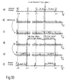
- Fig. 10 the timing of different types of signals is shown in an overview. From top to bottom the processing of the horizontal sync signals is visualized beginning with the detected H sync signals in Fig. 10a. On the abscissa of all diagrams in Fig. 10 the time grows from left to right.
- Figs. 10a to 10c correspond to the illustration in Figs. 6b to 6d describing the output of the H sync detector 23 (Fig. 2).
- the output signals H I and ⁇ I are provided to H-filter 24 to generate the filtered signals H o and ⁇ o (Figs. 10d, 10e) supplied to the ⁇ P 19 and the pixel interpolation filter 9, respectively.
- Fig. 10f the filtered H pulse (Fig. 10f) is supplied to the deflection driver 22 (Fig. 2).
- Fig. 10 also illustrates the effect of the time delay.
- a line delay corresponds to case b) in Fig. 10b, where the estimation time point is approximately seven lines in the past, referring to the actual detected H sync pulse.
- This configuration is adapted to the present embodiment having eight lines of video memory.
- the size of the memory and the parameters of the line delay may be different in other embodiments of the invention.
- the line delay following the vertical signal processing block is needed to compensate the line delay of the video streams (Y/C or composite video) and uses the same delay time as the video stream line delay.
- the realization of the line delay for the vertical signal needs much less hardware; it is a binary signal (V-Imp, Field).
- the present embodiment of the invention uses a free-running output clock frequency and outputs a fixed number of pixels per line. Depending on the variation of horizontal and vertical input frequency, the number of lines per each output field can vary. Field synchronization is possible by changing the number of output lines per field. Therefore, this mode is ideally suited to drive CRTs for the following reasons.
- the maximum needed line buffer size is defined by the maximum difference between the input and output memory addresses during one field. Hence, for a maximum averaged H-frequency variation of ⁇ 0.5% including phase-skips at the writing and constant output H-frequency at the reading, the line buffer memory size must at least be capable to store three video lines.
- the implementation of the vertical synchronization with changing vertical frequency in CRT-TVs does not present difficulties for a person skilled in the art. This type of synchronization can also be used for other display technologies like LCD or plasma displays.
- Fig. 11 shows a comparison between the conventional PLL, a system based on a linear regression filter technique without video line memory and with four lines of video memory and finally the actual new approach based on the FIR filter technology.
- Fig. 11a shows the time-base variation tracking and Fig. 9b the noise suppression.
- Fig. 11a shows the error transfer function
- the error at typical distortion frequencies at approximately 30 Hz must be in the order of - 60 dB to avoid visible jitter.
- Fig. 11 shows a comparison between the conventional PLL, a system based on a linear regression filter technique without video line memory and with four lines of video memory and finally the actual new approach based on the FIR filter technology.
- Fig. 11a shows the time-base variation tracking and Fig. 9b the noise suppression.
- Fig. 11a shows the error transfer function
- 11b details the improvement of sync-noise suppression compared to PLL and also compared to the previous patent application.
- the filter quality is in between the symmetrical FIR filter and the linear regression without memory. This is a suitable solution for one to approximately five line delays or line memory resulting in asymmetrical FIR coefficients.
- Fig. 12 a diagram shows the asymmetrical and symmetrical impulse responses corresponding to filter coefficients of the various filter types described above.
- the + symbols indicate the coefficients for linear regression without memory;
- the x symbols indicate the coefficients for linear regression with a memory having a size of four lines;
- the * symbols indicate the coefficients for a symmetrical FIR filter and
- the dots indicate the coefficients of a conventional PLL design with a fast time constant and infinite impulse response.
- the indices of the filter coefficients are plotted. It is noted that the linear regression with and without memory and the PLL filter represent asymmetric filters in contrast to the symmetrical FIR filter.
- Fig. 13 gives a rough impression about the achievable improvement.
- a reference measurement is made with Philips SAA7113H mounted on an original Philips evaluation board.
- Fig. 13b shows the response of the proposed algorithm using a symmetrical FIR filter.
- the phase jump response is reduced to 50%. After the phase jump very good stability is achieved and no comb structure due to phase differences in different picture is visible. In addition, also the noise suppression is much better.
Abstract
A method for obtaining line synchronization
information items from a video signal is proposed. The
inventive method is based on convolving the relevant part
of a video line signal with a pattern function. The
result of the convolution operation is further processed
to determine the time instants of the occurrence of the
horizontal sync signals. The time instants are
subsequently filtered to generate horizontal pulses. A
video line memory allows to utilize subsequent horizontal
sync signals for calculating the horizontal sync pulse of
a current video line.
The invention also relates to an apparatus for
carrying out the method.
Description
- The invention relates to a method for obtaining line synchronization information items from a video signal. According to a second aspect the invention is related to an apparatus for generating a line synchronisation pulse for a video line signal.
- In today's television receivers and computer TV cards it is necessary to separate synchronisation signals (or in short: sync signals) to achieve a proper representation of the video image on the display, e.g. a cathode ray tube.
- Even though digital system solutions will become increasingly predominant in future television technology, analogue source signals will still exist for many years in the future. Examples include the terrestrial reception of video signals, which is still widespread to date, and the analogue recording methods, e.g. according to the VHS standard in the case of video recorders. Such analogue signal sources represent critical signal sources for digital systems, and their signal processing requires special measures. The situation is the same for future multimedia terminals as long as they are equipped with an analogue video input. Due to the existence of large quantities of analogue video material, e.g. VHS tape libraries, it is unlikely that the use of analogue video signals could disappear in the near future.
- Conventionally, a sync slicer is used for sync separation. The sync slicer is combined with a PLL (Phase Locked Loop) for "smoothing" the extracted sync information. The PLL technology is mature but has well known limitations due to two conflicting requirements: On the one hand the PLL must have a low-pass characteristic to suppress disturbances in the sync signal detection caused by noise. On the other hand, tape recorders, in particular camcorders, output the video signal on a variable time base due to mechanical tolerances.
- The time base variations also appear as disturbances of the sync signal to the PLL. However, this kind of disturbance has to be passed through without attenuation because any alterations of the time base would create horizontal instabilities of the displayed video picture. In other words: The PLL has to suppress noise on the one hand and has to pass time-base variations on the other hand. Fortunately, the two effects are distinguishable by their frequency. Time-base variations are a low frequency effect above 1 kHz. As the PLL is always a second order loop, corner frequencies and stability are selected in every new designed system for best compromise.
- Television receivers with digital signal processing (e.g. in the case of the 100 Hz technology) have been operating, as a rule, with clock systems, which are synchronized with the respective input signal. Since the input signal is the analogue CVBS signal, either the horizontal sync pulse (line-locked clock) or, alternatively, the colour subcarriers or colour synchronizing pulses (burst) (colour subcarrier-locked clock) are frequently used as reference point for the synchronization. The sync separation in the video lines has usually been carried out to date by means of analogue methods using so-called sync separator stages and a PLL filter stage connected downstream. In television receivers with digital signal processing, a PLL filter stage, which is a digital realization of the known analogue sync signal processing is commonly used. The filter stage is then a digital PLL (Phase-Locked Loop). Examples of such digital PLL circuits are the circuits SAA 7111 from Philips, HMP 8112 from Harris and Digit 3000 from Micronas. The principal problem with such digital PLL circuits is that the known instabilities in the picture occur when the input signal present is an analogue video signal picked off from an analogue video recorder, which is currently operating in the search mode (fast forward or reverse run). Many users of analogue video recorders are sufficiently acquainted with such instabilities. Specifically, disturbing horizontal stripes appear in the picture when the video recorder is operating in the search mode. These disturbing stripes originate from the fact that in the search mode, the video heads no longer run on a single slanted track but rather sweep across two or more slanted tracks, depending on the search speed. During the transition from one slanted track to the next, abrupt sudden phase changes arise with regard to the occurrence of the sync pulses of the video lines. These sudden phase changes are actually governed by the geometry in magnetic tape recording in accordance with the slanted track method. The sudden phase changes are therefore determined by the system and, in addition, virtually unavoidable.
- Irregular occurrence of line sync pulses also arises, however, in the case of video signals generated by camcorders. In this case, the instabilities that occur are, as a rule, more severe than in the case of a normal video recorder, because the regulation of the head-drum speed is subject to greater fluctuations on account of the larger component tolerances.
- EP-A 0 266 147 discloses a digital PLL circuit for a television receiver. In the case of this digital PLL circuit, in order to avoid the abovementioned problem in the search operating mode in video recorders, a switching unit is provided which drastically shortens the time constant of the phase-locked loop in the event of identification of a sudden phase change caused by the head changeover at the end of a slanted track, with the result that the region of instability in the picture is reduced in size. The disadvantage of this solution is that the reduction of the time constant of the phase-locked loop provided by this solution means that noise components in the video signal are able to be suppressed less well and disturbing lines still remain visible, even though to a lesser extent than when the time constant is larger.
- In EP-
A 0 899 945 a method is for obtaining line synchronization information is described. According to the known method a video line is convoluted with an idealized horizontal synchronization pulse. The result of the convolutions processed in an open loop system replacing the PLL. The open loop system is realized by a linear regression to extrapolate the best guess of a current sync pulse using past sync pulses. - Convolving, or convolution, is a well-known term meaning the integral of one function multiplied by another function, which is shifted in time, see for example in "New IEEE Standard Dictionary of Electrical and Electronics Terms", 1993.
- Using the known systems as a starting point it is desirable to have a method providing an even better performance with regard to horizontal synchronization of the video lines.
- The present invention suggests a method for obtaining line synchronization information from a video line signal. According to the inventive method the relevant part of the video line signal is analysed to determine time instants defining the temporal position of the line synchronization pulses. A predetermined number of video lines is stored in a line delay. Using this as a data base a filtered time instant for a video line preceding the currently received video line by the number of video lines stored in the line delay.
- In an embodiment of the invention the calculation is an interpolation of the time instants determined for video lines preceding and following the currently displayed video line. Specifically, in another embodiment the interpolation is a linear interpolation.
- In order to define the time instants of the synchronization pulses precisely it is suggested to convolute the entire or relevant part of the video line with a pattern function. An idealized synchronization pulse may be used as the pattern function.
- According to the second aspect of the invention an apparatus for generating line synchronization pulses from a video line signal is suggested. The inventive apparatus comprises means for analysing the entire or the relevant part of the video line to determine time instants defining the temporal position of the line synchronization pulses. The apparatus further includes a line delay for storing a number of video lines. Finally, means are provided for calculating a filtered time instant for a video line preceding the currently received video line by the number of video lines stored in the line delay.
- In another embodiment the apparatus comprises means for convolving the entire or the relevant part of the video line with a pattern function.
- In yet another embodiment the apparatus is provided with an FIR filter having a set of predetermined filter constants.
- Exemplary embodiments of the invention are illustrated in the drawings and are explained in more detail in the following description. In the figures it is shown:
- Fig. 1
- simulated results for the reciprocal of the current horizontal frequency of line sync pulses in a video signal, which has been picked off from a camcorder;
- Fig. 2
- a top level block diagram for baseband sync and video processing;
- Fig. 3
- a diagrammatic illustration of a convolution operation of two square-wave pulses;
- Fig. 4
- the structure of an MTA filter (moving time average) for carrying out the convolution operation;
- Fig. 5
- a diagrammatic illustration for the calculation of the zero of the first derivative of the result function of the convolution operation according to the invention;
- Fig. 6
- a graphical illustration of the timing of the video signal, the horizontal sync signal and the system clock;
- Fig. 7
- the time positions of the horizontal sync pulses, a schematic structure of the FIR filter and a graphical representation of the used filter coefficients;
- Fig. 8
- the circuit section handling the time management of the synchronisation signal processing;
- Fig. 9
- the timing of the counters incorporated in the time management circuit section;
- Fig. 10
- the time positions of the detected Hsync pulses, the output pulses of the Hsync detector and the output pulses of the horizontal filter;
- Fig. 11
- a comparison of the error transfer function and transfer function of different types of Hsync processing means;
- Fig. 12
- the filter coefficients of different types of filters, and
- Fig. 13
- a video picture exemplifying the improvement of the invention.
- Simulated values for the position of the line sync pulses in a video signal are plotted in Fig. 1. The number of the respective line is plotted in the direction of the abscissa in Figure 1. The reciprocal of the current
horizontal frequency 1/fH for the line sync pulses is plotted in the direction of the ordinate of Fig. 1. The letter "n" generally designates the line number of each video line. The plotting of the reciprocal of the current horizontal frequency means that the time-domain positions of the respective line sync pulses can be compared with one another. The values corresponding to the actual measured values for the individual positions of the line sync pulses are in each case specified by the broken vertical lines. The end of each broken vertical line then specifies the line sync pulse position established. If the video signal present were ideal, then all of the broken lines would have the same length. The illustration is made for a video signal generated by a camcorder. Fluctuations in the line sync pulse positions about an average value are clearly discernible in a first region of Fig. 1. A steady increase in the line sync pulse positions can be discerned in a second part of Fig. 1. This behaviour can be explained by the regulation of the speed of rotation of the head-drum, this regulation being slow to start. Component tolerances and noise may be responsible for the variations of the line sync pulses about an average value. The crosses in Fig. 1 specify the line sync pulse positions corrected by the PLL circuits, which are usually used in the television receivers. However, the regulating behaviour of this PLL circuit results in the outputting of a phase error with regard to the line sync pulse positions as long as the vertical frequency in the video signal steadily changes. This is clearly discernible in the second part of Fig. 1 from the difference between the crosses and the broken lines. Since the sign of this phase error may be randomly distributed in the individual sub pictures and, in addition, the value of the phase error likewise does not always remain constant, the phase deviation D is manifested as a visible disturbance in the video picture displayed. The disturbance corresponds to a horizontal jitter effect in large parts of the picture. The picture gives the impression that somebody is shaking it in the horizontal direction. In order to eliminate the phase error with frequency changes occurring in the video signal, it is customary in the case of an analogue PLL control loop to increase the bandwidth of the PLL circuit. If this measure is taken, then the line sync pulse positions, which are indicated by circles in Fig. 1 are produced. However, this solution has the disadvantage that the noise suppression of the PLL circuit is impaired, as a result of which momentary picture disturbances in the form of a jitter behaviour are still discernible. Vertical lines no longer appear straight but rather distorted. - Fig. 2 shows a top level diagram of the sync and video processing of a TV incorporating the present invention.
- The proposed architecture is based on a free running system clock, e.g. a crystal oscillator. Hence, the system clock has no correlation to the video sync or colour subcarrier frequencies. The free running system clock is particularly advantageous for processor-based systems adapted to receive video signals of various types and properties. However, colour burst-locked clocked systems are also possible to realize with the architecture described in the following if this is desirable for certain embodiments.
- On the left hand side of Fig. 2 the inputs for analogue base band video signals are shown. The inputs 1a and 1b are used for S video signals having separate chrominance C and luminance Y inputs. The
input 2 is provided for receiving composite video signals. The analogue video signals are converted into corresponding digital signals by A/D converters - In the signal path processing the composite video signal a comb filter is provided to separate the luminance Y and the chrominance C signals. Subsequently, the signals are fed into a chrominance decoder to generate the luminance signal Y and the chrominance signal C.
- A
switch 8 is controlled to select the luminance and chrominance signals received fromline delay 4a or fromchroma decoder 7 to be further processed in a pixel interpolation filter 9, which will be described in more detail below. - The output of filter 9 is buffered in a
line buffer 11 and passed on to acolour dematrix 12 for generating digital R, G, B signals. The digital R, G, B signals are converted into analogue signals, amplified by associated drivers inblock 13 and supplied to acathode ray tube 14 for display. - In case a display device different than a CRT, e.g. an LCD, TFT or plasma display is used, the signal processing may be different than shown in the present embodiment. However, these differences do not depart from the scope of the present invention.
- For synchronization signal processing a digital luminance signal Y or a digital composite video signal is selectively used depending on which analogue inputs are active. The signal for sync signal processing is selected by
switch 16 controlled by the same control signal as theswitch 8. The vertical sync processing inblock 17 is conventional and is therefore not described in more detail. The information regarding which field of a video frame is currently being processed is also obtained in this unit. The vertical sync signal Vsync is delayed in aline delay 18 to re-establish the timing to the video signals delayed in the line delays 4a and 4b, respectively. - The Vsync signal is input to a
microprocessor 19, which is among other functions operative to execute the synchronization logic. - In a Hsync processing unit 21 the Hsync signals are detected and processed by the inventive method, which will be described in more detail below. The horizontal sync information is supplied to the
µP 19. TheµP 19 uses the horizontal and vertical sync information to generate output signals for adeflection driver 22 being connected to a deflection apparatus not shown in Fig. 2. - The deflection apparatus is associated with the
CRT 14 and effects the scanning of the electron beams inside the CRT in a conventional way. - In case the display device is not a CRT the
deflection driver 22 is replaced by an appropriate device effecting the representation of the video signal line by line on the screen of the respective display device. - The Hsync processing unit 21 comprises a Hsync detector 23 to determine the timing of Hsync signals contained in the received video signal. The Hsync signals are filtered in a H-
filter 24 and the resulting signals Ho and ϕo are provided to the µP19 and to the pixel interpolation filter 9. The operation of the Hsync detector 23, the H-filter 24 and the Vsync processor 17 is controlled by anevent control 25, which will be described in more detail in connection with Fig. 8. - In contrast to the otherwise widespread edge detection for the falling edge of a line sync pulse in the CVBS signal, the present Hsync detector 23 operates according to the correlation principle. In this case, the CVBS signal is convolved with an ideal line sync pulse and then the minimum is sought. This principle is illustrated in Fig. 3, where it is possible to discern in principle that the convolution operation of two square-wave pulses generates a triangle function as result function. This function then has a minimum or maximum, which specifies the position of the line sync pulse. The CVBS signal for a video line is designated by the reference symbol fin(k). The reference symbol sideal (k) designates an ideal line sync pulse. The result function of the convolution operation is designated by the reference symbol ϕSV(k). The reference symbol kS specifies the position of the minimum of the result function. The convolution operation is carried out in the Hsync detector 23 for example in such a way that the CVBS signal present in one of the line stores 4a, 4b for a video line is digitally convolved with a corresponding ideal line sync pulse. The execution may alternatively be configured in such a way that instead of the CVBS signal for the entire video line being convolved with the ideal line sync pulse, only the relevant part for the line sync pulse is convolved with the idealized line sync pulse.
- This detection method behaves extremely robustly even for example in the case of terrestrial signals with multipath propagation which are subjected to a great deal of interference. If a constant correlation length lS is used for the convolution operation, the MTA (Moving Time Average) filter known from the prior art is suitable, for example for the circuitry realization of the convolution operation, the structure of which filter is illustrated in Fig. 4, where the line sync pulse is represented in an idealized manner with a square-wave pulse response.
- In order to determine the maximum or minimum in the result function of the convolution operation, the zero of the first derivative of the result function is calculated. This computation operation is illustrated in more detail in Fig. 5, where the reference symbol ϕ ˙SV (k) designates the first derivative of the result function, the variable k stands for the respective sample of the derivative function, kS specifies the position of the zero of the derivative and k0 specifies the last sample with a negative sign in the transition region of the first derivative of the result function. For an exact determination of the zero, a linear regression is carried out in the transition region of the derivative function. The zero is then calculated in a simple manner using the regression line established. The point of intersection of the regression line with the zero axis is designated by the reference symbol Ns in Figure 5. The regression length lv amounts to nine samples in the example illustrated. In this way, the minimum of the first derivative is calculated with subpixel resolution. The subpixel resolution is necessary since the subsequent vertical filtering cannot effectively eliminate pixel quantization. The subpixel resolution is also necessary because, e.g. given a sampling rate of 18 MHz for the A/D conversion in the A/
D conversion unit 20 and a display having a width of 56 cm, the visibility limit for picture details is approximately 0.17 pixel. Investigations with various input signals have shown that a linear regression yields an optimum result for the calculation of the subpixel resolution. For the calculation of the centre of the line sync pulse, which corresponds to the minimum of the result function of the convolution operation, approximately 10 samples are sufficient for the region around the zero of the derivative function. The computation rule that approximately 10 samples are sufficient was established at a sampling rate of 18 MHz using video signals having a constant horizontal frequency for various signal-to-noise ratios in the case of terrestrial reception. In this case, the standard deviation for a signal having a signal-to-noise ratio of 15 dB was 0.93 pixel. In the case of a low-noise signal having a signal-to-noise ratio of 35 dB, the standard deviation is 0.07 pixel. - If video signals originating from video recorders are processed, the horizontal frequency can deviate by up to 4% in the trick mode in video recorders, which also proportionally affects the length of the line sync pulse. This is then manifested in a deterioration in the identifiability of the edge in the course of the derivative function of the result function of the convolution operation. However, it has been shown that deviations up to this degree have no relevant influence on the detection accuracy in the course of the zero determination. For the calculation of the centre kS of the line sync pulse by means of linear regression, it is possible to use an arithmetic unit instead of a more complex microprocessor, since approximately 32 µs remain for this calculation, which corresponds to half of one video line in the PAL system. Moreover, the equidistant samples enable a distinct simplification of the calculation. The formula for the calculation of the centre ks of the line sync pulse with subpixel accuracy then reads as follows:

- In this case, kl is a constant, which can be calculated as a function of the
regression length 1. All the other symbols are known from the description regarding Figures 5 and 3. - Following the time base described in connection with Fig. 6 each video line duration TH can be calculated by the following equation:
- For an undistorted PAL standard input signal the line duration is TH = 64 µs. With a constant system clock frequency of fclk = 18 MHz the number of clock cycles between two Hsync pulses would be constant at ΔHI = 1152. The phase difference between the Hsync pulses and the beginning of a clock cycle would also be a constant value for all video lines.
- However, in practice the video line duration is not constant but variable. Noise and low frequent distortions are super imposing the input video signal causing a time shift of the detected temporal position of the Hsync pulse.
As a consequence the detected video line duration TH changes line by line causing horizontal jitter. To avoid this kind of jitter it is necessary to filter the detected temporal positions of the Hsync pulses. - For each time instant tn the Hsync detection block 23 outputs two values, HI and ϕI. HI describes the time difference between two Hsync pulses measured in integer cycles of the internal system clock. ϕI represents a fraction of one cycle allowing to determine the temporal position of a specific Hsync pulse with subpixel resolution.
- In Fig. 6 the details of the timing of the different signals are shown. Fig. 6a displays an analogue composite video signal CVBS with incorporated Hsync pulses, which are indicated by "H". Fig. 6b illustrates the temporal position ti of the Hsync pulses by
vertical lines 25. The abscissa in Fig. 6b is divided into units of the nominal duration TH of a video line. The temporal position ti falls into a particular cycle of the system clock. The relevant cycles define the integer number HI. A comparison between Figs. 6b and 6c illustrates that the nominal beginning of a video line as shown in Fig. 6b coincides with the beginning of a cycle of the system clock as illustrated in Fig. 6c. However, Fig. 6b also shows that the temporal positions ti of the detected Hsync pulses do not coincide with a cycle of the system clock. The time shift also discernible in Fig. 6b as a deviation from the nominal beginning of a video line is quantified by ϕI. ϕI defines the fraction of a system clock cycle the respective Hsync pulse lags behind the clock cycle. - Several examples of the time shift are illustrated in Fig. 6d with reference to Fig. 6c.
- The time instants ti determined according to the described method are subsequently filtered in a
horizontal filter 24. Thehorizontal filter 24 is a FIR filter having symmetrical filter coefficients. - At a given time the
FIR filter 24takes 1 line durations ΔTn, n=0, ..., 1 into account to calculate the filter output Tm as it is illustrated in Fig. 7a. One line duration ΔTn is the time difference between two Hsync pulses n and n+1, defined by the time instants tn and tn+1. - The FIR filter then calculates the filter output signal according to the equationwhere Cn,l are the filter coefficients, (1+1) is the filter length, and tn the time instants of the Hsync pulses. In Fig. 7b the

FIR filter 24 is shown in more detail. The time instants are stored in delay stages 26-1...26o. The contents of the delay stages is multiplied with the associated filter coefficient cn,m inmultipliers 27-1...27o. The individual products are summed up in anadder 28 to yield the filter output Tm. The index m of the calculated filter output Tm is related to the number of video lines that can be stored in theline delay 4a or 4b. In the present embodiment the line delay has a size of eight video lines and therefore m = 7. In other embodiments having a different size of line delay m may take a different value. - It is important to note that this filter design does not contain any feedback of a previous result to a subsequent result. The output of the horizontal filter depends exclusively on the input signals, i.e. the detected time instants ti. The H-
filter 24 is an open loop filter. - The horizontal filter outputs the filtered temporal position of the Hsync pulse in terms of values Ho and ϕo indicating the length of the video line in terms of a number of system clock cycles and a phase shift relative to the system clock, respectively. The time correction of the video signal is done by the pixel interpolation filter block 9, which is arranged to shift each video line in time with subpixel resolution corresponding to the value of ϕo, wherein o ≤ ϕo ≤ 1. The output signal Ho of the H filter defines the start of each new video line with the accuracy of one system clock cycle.
- In the previous paragraphs it has been shown that the HI pulse in connection with the additional phase information ϕI is used as input for the H-
filter 24. The summed up time information of each Hsync pulse (ΔHI + ϕI) is stored for a defined number of lines, which equals the FIR filter length. - In the present embodiment of the inventive apparatus the time measurement is implemented by means of counters, requiring only a few basic hardware components. A practical realization is shown in Fig. 8.
- Fig. 8 shows in more detail the circuit section being effective for the time management. The time management circuit section, which is referenced as a whole with the
reference number 31, is structured into several blocks comprising acounter block 32, acomparator block 33, aphase memory 34, theFIR filter 24 and anevent control 25. The details of theFIR filter 24 have already been described in connection with Fig. 7b. - The
counter block 32 includes twocounters 36a, 36b to measure the time difference between the occurrences of two subsequent HI signals in units of clock cycles. The HI signal is also supplied to theevent control 25 outputting a counter reset signal. During normal operation the counter reset signal corresponds the HI signal. - A
counter control unit 37 controls a switch 38 to connect the counter reset signal emitted by theuP 19 with either counter 36a orcounter 36b for resetting it. At the same time thecounter control unit 37 operates two further switches 39a and 39b to connect the output of the respective counter, which is not reset to one input of a comparator 41. The second input of the comparator 41 is provided with the predicted value calculated in the H-filter 24. The calculation is based on past and future HI values. If the two input values of the comparator 41 are equal it outputs the Ho pulse. - Fig. 9 shows the timing of the HI signal, the H0 pulse and the contents of the
counters 36a, 36b. One counter counts each HI pulse and the other counts the number of clock cycles for counter memory storage (circle) and output comparison (cross) and vice versa. Or in other words: The selected counter for output comparison counts the number of clock cycles from the last input pulse HI until the output pulse is generated by the prediction value (cross in Fig. 9). At the same time the selected filter is reset. Fractions of a clock cycle are not important for the counter time scheme. Fractional parts of a clock cycle are stored in thephase memory 34. - Some lines of delay/memory are needed for the new horizontal filter technique based on an interpolation principle. In this example, a 8 line delay block is used to delay the video signal by 8 video lines. This is needed, because the signal delay allows the H filter block to obtain timing information from past video lines (still stored in line memory), before the video signal is output to the pixel interpolation filter. After passing the pixel interpolation filter, the video lines are orthogonalized with the processed timing information of the H filter and further time corrections are not possible. Using this line delay, the filter behavior can be improved as shown in the next chapter.
- In Fig. 10 the timing of different types of signals is shown in an overview. From top to bottom the processing of the horizontal sync signals is visualized beginning with the detected Hsync signals in Fig. 10a. On the abscissa of all diagrams in Fig. 10 the time grows from left to right. Figs. 10a to 10c correspond to the illustration in Figs. 6b to 6d describing the output of the Hsync detector 23 (Fig. 2). The output signals HI and ϕ I are provided to H-
filter 24 to generate the filtered signals Ho and ϕo (Figs. 10d, 10e) supplied to theµP 19 and the pixel interpolation filter 9, respectively. - Finally, the filtered H pulse (Fig. 10f) is supplied to the deflection driver 22 (Fig. 2). Apart from the timing, Fig. 10 also illustrates the effect of the time delay. Using a line delay corresponds to case b) in Fig. 10b, where the estimation time point is approximately seven lines in the past, referring to the actual detected Hsync pulse. This configuration is adapted to the present embodiment having eight lines of video memory. Of course, the size of the memory and the parameters of the line delay may be different in other embodiments of the invention. The line delay following the vertical signal processing block is needed to compensate the line delay of the video streams (Y/C or composite video) and uses the same delay time as the video stream line delay. The realization of the line delay for the vertical signal needs much less hardware; it is a binary signal (V-Imp, Field).
- The last building blocks "Line-Memory Dual-Port" and "Synchronization-Logic" are used to synchronize the output signals for different display techniques.
- The present embodiment of the invention uses a free-running output clock frequency and outputs a fixed number of pixels per line. Depending on the variation of horizontal and vertical input frequency, the number of lines per each output field can vary. Field synchronization is possible by changing the number of output lines per field. Therefore, this mode is ideally suited to drive CRTs for the following reasons.
- i) Tube displays are horizontally stable, when the horizontal frequency of the driver stage is essentially constant (crystal locked).
- ii) DC-coupled vertical CRT driver stages are able to adapt to changing line numbers per field without any visible degradation.
- iii) This mode is also compatible with future multimedia-systems, where the usage of a line-locked clock system might be not acceptable.
-
- A constant horizontal (Hsync) frequency can be obtained by the proposed sync algorithm, when some lines of buffer memory are used to compensate the different line durations TH between the buffer input and output during one field (TH ≠ const., TH,out = const.).
- This corresponds to a variation of the number of pixels per line at the buffer input and a constant number of pixels per line at the buffer output as it is shown in Fig. 4.5. ???
- The vertical coupling is field synchronous. This means, that the vertical frequency of the output adapts at the end of each field to the vertical timing of the input to obtain correct field synchronization (TV = TV,out ≠ const.). The maximum needed line buffer size is defined by the maximum difference between the input and output memory addresses during one field. Hence, for a maximum averaged H-frequency variation of ±0.5% including phase-skips at the writing and constant output H-frequency at the reading, the line buffer memory size must at least be capable to store three video lines. The implementation of the vertical synchronization with changing vertical frequency in CRT-TVs does not present difficulties for a person skilled in the art. This type of synchronization can also be used for other display technologies like LCD or plasma displays.
- It is noted that the use of a video line memory according to the invention for the purpose to take into account subsequent horizontal sync pulses is not limited to the use of FIR filters. The same concept can be applied with linear regression as filtering function. Filtering by linear regression with different regression lengths is disclosed in EP-
A 0 899 945. In combination with the video line memory the known filter concept allows "to look into the future" to yield improved horizontal filtering. The results achieved by the different techniques will be discussed further below. - The advantage of the new approach can be seen best in the "frequency domain". Fig. 11 shows a comparison between the conventional PLL, a system based on a linear regression filter technique without video line memory and with four lines of video memory and finally the actual new approach based on the FIR filter technology.
Fig. 11a shows the time-base variation tracking and Fig. 9b the noise suppression. To get a relevant measure of the tracking quality of the sync separation, Fig. 11a shows the error transfer function | 1-He(f) |, where He(f) is the transfer function of the FIR filter. The error at typical distortion frequencies at approximately 30 Hz must be in the order of - 60 dB to avoid visible jitter. Fig. 11b details the improvement of sync-noise suppression compared to PLL and also compared to the previous patent application. Alternatively, when approximating the Linear Regression by a FIR filter the filter quality is in between the symmetrical FIR filter and the linear regression without memory. This is a suitable solution for one to approximately five line delays or line memory resulting in asymmetrical FIR coefficients. - In Fig. 12 a diagram shows the asymmetrical and symmetrical impulse responses corresponding to filter coefficients of the various filter types described above. The + symbols indicate the coefficients for linear regression without memory; the x symbols indicate the coefficients for linear regression with a memory having a size of four lines; the * symbols indicate the coefficients for a symmetrical FIR filter and finally the dots indicate the coefficients of a conventional PLL design with a fast time constant and infinite impulse response. On the abscissa of the diagram in Fig. 12 the indices of the filter coefficients are plotted. It is noted that the linear regression with and without memory and the PLL filter represent asymmetric filters in contrast to the symmetrical FIR filter.
- Instability in video cannot be printed on paper, however, Fig. 13 gives a rough impression about the achievable improvement. A reference measurement is made with Philips SAA7113H mounted on an original Philips evaluation board. Fig. 13a shows the phase-jump response of a synthetically generated VCR search mode and the noise response (SNR = 12dB). The typical instability between two phase jumps seen here as offset between two fields as a comb structure is clearly discernible. The comb structure is marked in Fig. 13a by ovals.
- Fig. 13b shows the response of the proposed algorithm using a symmetrical FIR filter. The phase jump response is reduced to 50%. After the phase jump very good stability is achieved and no comb structure due to phase differences in different picture is visible. In addition, also the noise suppression is much better.
Claims (10)
- Method for obtaining line synchronization information from a video line signal comprising the following steps:a) analyzing the entire or the relevant part of the video line signal to determine time instants (ti) defining the temporal position of the line synchronization pulses included in the video line signal,b) storing a predetermined number of video lines in a line delay, andc) calculating a filtered time instant (Tm) for a video line preceding the currently received video line by the number (m) of video lines stored in the line delay.
- Method according to claim 1, characterized bya) convolving the entire or the relevant part of the video line signal with a pattern function to generate a result function of the convolution operation andb) analyzing the result function (sv (k)) of the convolution operation of step a) to determine time instants (ti) defining the temporal position of the line synchronization pulse.
- Method according to claim 2, characterized by using an idealized line synchronization pulse as the pattern function.
- Method according to claim 1, characterized by calculating the filtered time instant (Tm) for a currently displayed video line by interpolation of the time instants determined for video lines preceding and following the currently displayed video line.
- Method according to claim 4, characterized by calculating the filtered time instant (Tm) for a currently displayed video line by linear interpolation of the time instants determined for video lines preceding and following the currently displayed video line.
- Method according to claim 1, characterized by filtering the time instants (ti) by an FIR filter having a set of predetermined filter constants (cn,1).
- Method according to claim 6, characterized by storing the defined time instants (ti) in associated delay elements,
wherein the time instants represent the time constant of the delay element, and
wherein the delay elements are incorporated in the FIR filter (24). - Apparatus for generating a line synchronization pulse from a video line signal, comprising:a) means for analyzing the entire or the relevant part of the video line signal to determine time instants (ti) defining the temporal position of the line synchronization pulse included in the video line signal,b) a line delay for storing a predetermined number (m) of video line signals, andc) means for calculating a filtered time instant (Tm) for a video line preceding the currently received video line by the number (m) of video lines stored in the line delay.
- Apparatus according to claim 8, characterized by means for convolving the entire or the relevant part of the video line signal with a pattern function.
- Apparatus according to claim 8, characterized by an FIR filter having a set of predetermined filter constants (Cn,l).
Priority Applications (9)
| Application Number | Priority Date | Filing Date | Title |
|---|---|---|---|
| EP01401811A EP1274229A1 (en) | 2001-07-06 | 2001-07-06 | Method for obtaining line synchronization information items from a video signal, and apparatus for carrying out the method |
| EP02743237A EP1405503B1 (en) | 2001-07-06 | 2002-06-24 | Method for obtaining line synchronization information items from a video signal, and apparatus for carrying out the method |
| DE60214715T DE60214715T2 (en) | 2001-07-06 | 2002-06-24 | METHOD FOR OBTAINING LINE SYNCHRONIZATION INFORMATION OBJECTS FROM A VIDEO SIGNAL AND DEVICE FOR CARRYING OUT SAID METHOD |
| CNA028135849A CN1524375A (en) | 2001-07-06 | 2002-06-24 | Method for obtaining line synchronization information items from a video signal, and apparatus for carrying out the method |
| MXPA03011891A MXPA03011891A (en) | 2001-07-06 | 2002-06-24 | Method for obtaining line synchronization information items from a video signal, and apparatus for carrying out the method. |
| JP2003511533A JP2004534482A (en) | 2001-07-06 | 2002-06-24 | Method for obtaining a line synchronization information item from a video signal, and apparatus for implementing this method |
| KR10-2004-7000026A KR20040013092A (en) | 2001-07-06 | 2002-06-24 | Method for obtaining line synchronization information items from a video signal, and apparatus for carrying out the method |
| PCT/EP2002/006933 WO2003005704A1 (en) | 2001-07-06 | 2002-06-24 | Method for obtaining line synchronization information items from a video signal, and apparatus for carrying out the method |
| US10/483,033 US7271843B2 (en) | 2001-07-06 | 2002-06-24 | Method and apparatus for analyzing a digitally converted analogue signal |
Applications Claiming Priority (1)
| Application Number | Priority Date | Filing Date | Title |
|---|---|---|---|
| EP01401811A EP1274229A1 (en) | 2001-07-06 | 2001-07-06 | Method for obtaining line synchronization information items from a video signal, and apparatus for carrying out the method |
Publications (1)
| Publication Number | Publication Date |
|---|---|
| EP1274229A1 true EP1274229A1 (en) | 2003-01-08 |
Family
ID=8182799
Family Applications (2)
| Application Number | Title | Priority Date | Filing Date |
|---|---|---|---|
| EP01401811A Withdrawn EP1274229A1 (en) | 2001-07-06 | 2001-07-06 | Method for obtaining line synchronization information items from a video signal, and apparatus for carrying out the method |
| EP02743237A Expired - Lifetime EP1405503B1 (en) | 2001-07-06 | 2002-06-24 | Method for obtaining line synchronization information items from a video signal, and apparatus for carrying out the method |
Family Applications After (1)
| Application Number | Title | Priority Date | Filing Date |
|---|---|---|---|
| EP02743237A Expired - Lifetime EP1405503B1 (en) | 2001-07-06 | 2002-06-24 | Method for obtaining line synchronization information items from a video signal, and apparatus for carrying out the method |
Country Status (8)
| Country | Link |
|---|---|
| US (1) | US7271843B2 (en) |
| EP (2) | EP1274229A1 (en) |
| JP (1) | JP2004534482A (en) |
| KR (1) | KR20040013092A (en) |
| CN (1) | CN1524375A (en) |
| DE (1) | DE60214715T2 (en) |
| MX (1) | MXPA03011891A (en) |
| WO (1) | WO2003005704A1 (en) |
Cited By (2)
| Publication number | Priority date | Publication date | Assignee | Title |
|---|---|---|---|---|
| DE102005060701A1 (en) * | 2005-07-28 | 2007-02-08 | Rohde & Schwarz Gmbh & Co. Kg | Vertical synchronization time regulation method for transmitting image information as two half-images involves determining position of extreme value of folding function from signal section |
| US7782314B2 (en) * | 2003-05-29 | 2010-08-24 | Fujitsu Component Limited | Device and system for synchronizing image signals transmitted with superimposed signals |
Families Citing this family (2)
| Publication number | Priority date | Publication date | Assignee | Title |
|---|---|---|---|---|
| KR102200399B1 (en) * | 2014-12-04 | 2021-01-08 | 한화테크윈 주식회사 | Coaxial communications type receiver |
| CN113792371B (en) * | 2021-09-27 | 2024-01-26 | 江西科技学院 | Diagnosis method for track abnormal matching based on phase-locked value |
Citations (3)
| Publication number | Priority date | Publication date | Assignee | Title |
|---|---|---|---|---|
| US5594506A (en) * | 1995-09-26 | 1997-01-14 | Samsung Electronics Co., Ltd. | Line sync detector for digital television receiver |
| EP0796007A1 (en) * | 1996-03-13 | 1997-09-17 | Michael Johannes Koch | Lines and frame synchronization circuit for a digital video signal |
| EP0899945A2 (en) * | 1997-08-27 | 1999-03-03 | Deutsche Thomson-Brandt Gmbh | Method for obtaining line synchronization information items from a video signal, and apparatus for carrying out the method |
Family Cites Families (9)
| Publication number | Priority date | Publication date | Assignee | Title |
|---|---|---|---|---|
| US4220967A (en) * | 1976-09-27 | 1980-09-02 | Hughes Aircraft Company | Scene tracker using multiple independent correlators |
| JPS59229709A (en) * | 1983-06-10 | 1984-12-24 | Toshiba Corp | Picture information recorder |
| US5119193A (en) * | 1990-09-19 | 1992-06-02 | Nec Corporation | Video-signal processing device |
| US5594406A (en) * | 1992-02-25 | 1997-01-14 | Matsushita Electric Industrial Co., Ltd. | Zinc oxide varistor and process for the production thereof |
| US5404173A (en) * | 1993-03-10 | 1995-04-04 | Brooktree Corporation | Method to synchronize video modulation using a constant time base |
| US5515108A (en) * | 1993-08-18 | 1996-05-07 | Samsung Electronics Corporation | Digital automatic frequency control method and circuit therefor |
| DE4335197A1 (en) * | 1993-10-15 | 1995-04-20 | Thomson Brandt Gmbh | Synchronous signal separation circuit for a television receiver |
| KR0134309B1 (en) * | 1994-03-11 | 1998-04-23 | 김광호 | Digital frequence automatic control circuit |
| JPH08116466A (en) * | 1994-10-14 | 1996-05-07 | Fujitsu Ten Ltd | Synchronizing signal processing circuit |
-
2001
- 2001-07-06 EP EP01401811A patent/EP1274229A1/en not_active Withdrawn
-
2002
- 2002-06-24 EP EP02743237A patent/EP1405503B1/en not_active Expired - Lifetime
- 2002-06-24 CN CNA028135849A patent/CN1524375A/en active Pending
- 2002-06-24 DE DE60214715T patent/DE60214715T2/en not_active Expired - Lifetime
- 2002-06-24 WO PCT/EP2002/006933 patent/WO2003005704A1/en active IP Right Grant
- 2002-06-24 US US10/483,033 patent/US7271843B2/en not_active Expired - Fee Related
- 2002-06-24 JP JP2003511533A patent/JP2004534482A/en active Pending
- 2002-06-24 KR KR10-2004-7000026A patent/KR20040013092A/en not_active Application Discontinuation
- 2002-06-24 MX MXPA03011891A patent/MXPA03011891A/en active IP Right Grant
Patent Citations (3)
| Publication number | Priority date | Publication date | Assignee | Title |
|---|---|---|---|---|
| US5594506A (en) * | 1995-09-26 | 1997-01-14 | Samsung Electronics Co., Ltd. | Line sync detector for digital television receiver |
| EP0796007A1 (en) * | 1996-03-13 | 1997-09-17 | Michael Johannes Koch | Lines and frame synchronization circuit for a digital video signal |
| EP0899945A2 (en) * | 1997-08-27 | 1999-03-03 | Deutsche Thomson-Brandt Gmbh | Method for obtaining line synchronization information items from a video signal, and apparatus for carrying out the method |
Cited By (3)
| Publication number | Priority date | Publication date | Assignee | Title |
|---|---|---|---|---|
| US7782314B2 (en) * | 2003-05-29 | 2010-08-24 | Fujitsu Component Limited | Device and system for synchronizing image signals transmitted with superimposed signals |
| DE102005060701A1 (en) * | 2005-07-28 | 2007-02-08 | Rohde & Schwarz Gmbh & Co. Kg | Vertical synchronization time regulation method for transmitting image information as two half-images involves determining position of extreme value of folding function from signal section |
| DE102005060701B4 (en) * | 2005-07-28 | 2011-06-16 | Rohde & Schwarz Gmbh & Co. Kg | Method for determining vertical synchronization times |
Also Published As
| Publication number | Publication date |
|---|---|
| WO2003005704A1 (en) | 2003-01-16 |
| EP1405503A1 (en) | 2004-04-07 |
| DE60214715D1 (en) | 2006-10-26 |
| US7271843B2 (en) | 2007-09-18 |
| MXPA03011891A (en) | 2004-03-26 |
| US20040174461A1 (en) | 2004-09-09 |
| JP2004534482A (en) | 2004-11-11 |
| KR20040013092A (en) | 2004-02-11 |
| EP1405503B1 (en) | 2006-09-13 |
| DE60214715T2 (en) | 2007-02-22 |
| CN1524375A (en) | 2004-08-25 |
Similar Documents
| Publication | Publication Date | Title |
|---|---|---|
| US5786872A (en) | Motion detection circuit calculates difference between input video signal and one frame-period signal | |
| KR0126658B1 (en) | The sample rate conversion device for signal processing of non-standard tv. | |
| US4595953A (en) | Television receiver having character generator with burst locked pixel clock and correction for non-standard video signals | |
| EP0899945B1 (en) | Method for obtaining line synchronization information items from a video signal, and apparatus for carrying out the method | |
| US4667240A (en) | Timing correction circuitry as for TV signal recursive filters | |
| US6219105B1 (en) | Video signal processing apparatus | |
| KR940006626B1 (en) | Apparatus for detecting nonstandard video signals | |
| JPH03171984A (en) | Digital circuit device for processing analog video signal by means of self-running system lock | |
| EP1405503B1 (en) | Method for obtaining line synchronization information items from a video signal, and apparatus for carrying out the method | |
| US4977445A (en) | Sync-signal reproducing circuit for use in television receiver | |
| US5923377A (en) | Jitter reducing circuit | |
| US6801706B1 (en) | Jitter correcting apparatus and method for video signals | |
| US6462789B1 (en) | Circuit and method for generating chrominance lock | |
| JP3417154B2 (en) | Display device | |
| JPH07162808A (en) | Device and method for processing video signal and video signal recording and reproducing device | |
| KR930005339B1 (en) | Error correcting circuit for double azimus vtr when a change of speed | |
| CA2110602C (en) | Horizontal line counter stabilization in a video receiver | |
| JPH07312699A (en) | Digital video reproducing device | |
| JP2571038B2 (en) | Digital television signal processor | |
| KR0130812B1 (en) | Digital horizontal synchronous signal and phase error penetrator and its method | |
| JP2653351B2 (en) | Digital television receiver | |
| JP2517619B2 (en) | Television receiver | |
| JP3140202B2 (en) | Ghost removal device | |
| Rothermel et al. | Synchronization of analog video signals with improved image stability | |
| JP2002218278A (en) | Synchronizing separation circuit and method, display device and method and signal processing device and method |
Legal Events
| Date | Code | Title | Description |
|---|---|---|---|
| PUAI | Public reference made under article 153(3) epc to a published international application that has entered the european phase |
Free format text: ORIGINAL CODE: 0009012 |
|
| AK | Designated contracting states |
Kind code of ref document: A1 Designated state(s): AT BE CH CY DE DK ES FI FR GB GR IE IT LI LU MC NL PT SE TR |
|
| AX | Request for extension of the european patent |
Free format text: AL;LT;LV;MK;RO;SI |
|
| AKX | Designation fees paid | ||
| REG | Reference to a national code |
Ref country code: DE Ref legal event code: 8566 |
|
| STAA | Information on the status of an ep patent application or granted ep patent |
Free format text: STATUS: THE APPLICATION IS DEEMED TO BE WITHDRAWN |
|
| 18D | Application deemed to be withdrawn |
Effective date: 20030709 |